matseng
-
Video of the running WireZ80
01/08/2019 at 18:36 • 0 commentsAh right! I must have a video of it executing the, what I believe, 0xFF instructions. Who doesn't like some blinkenlights? :-)
-
Current status @ deadline
01/08/2019 at 18:30 • 0 commentsWell, it seems that I will not have time to add any firmware before the deadline, but it can at least either run NOPs (if the display/keypad-module is disconnected) or was looks like $FF's when it's connected.
I reduced the clock speed to 28KHz to get the address bus LEDs to flash prettily.
When the display unit is disconnected then the databus is giving just zeros to the Z80 when it runs and since 0x00 is a NOP for a Z80 it justs increments the addresses and fetches the next NOP all the way up to address 65535 when it wraps over to address 0 again.
By some reason the databus looks to end up as 0xFF when the display unit is connected and whatever instruction that is it looks like the addresses are decrementing instead. Maybe it's a relative branch to -1 that makes it go backwards? I haven't bothered to look it up yet.
So the Wirez80 seems to be in reasonably good working order, just lacking me writing some firmware for it. But that will take more than the 90 minutes remaning for the deadline so this is what y'all get from me this time.
I will of course spend some more time on the project to get it in a more working order with a "monitor" firmware to examine/deposit data to the memory and run code.

The WireZ80 running dummy instructions I'll definitely need to make some kind of acrylics enclosure for it that will keep it safe or else it might end up all squashed as my old "Lethal Nixie Cube" did when I stepped on it.
-
Hooking up tower and display
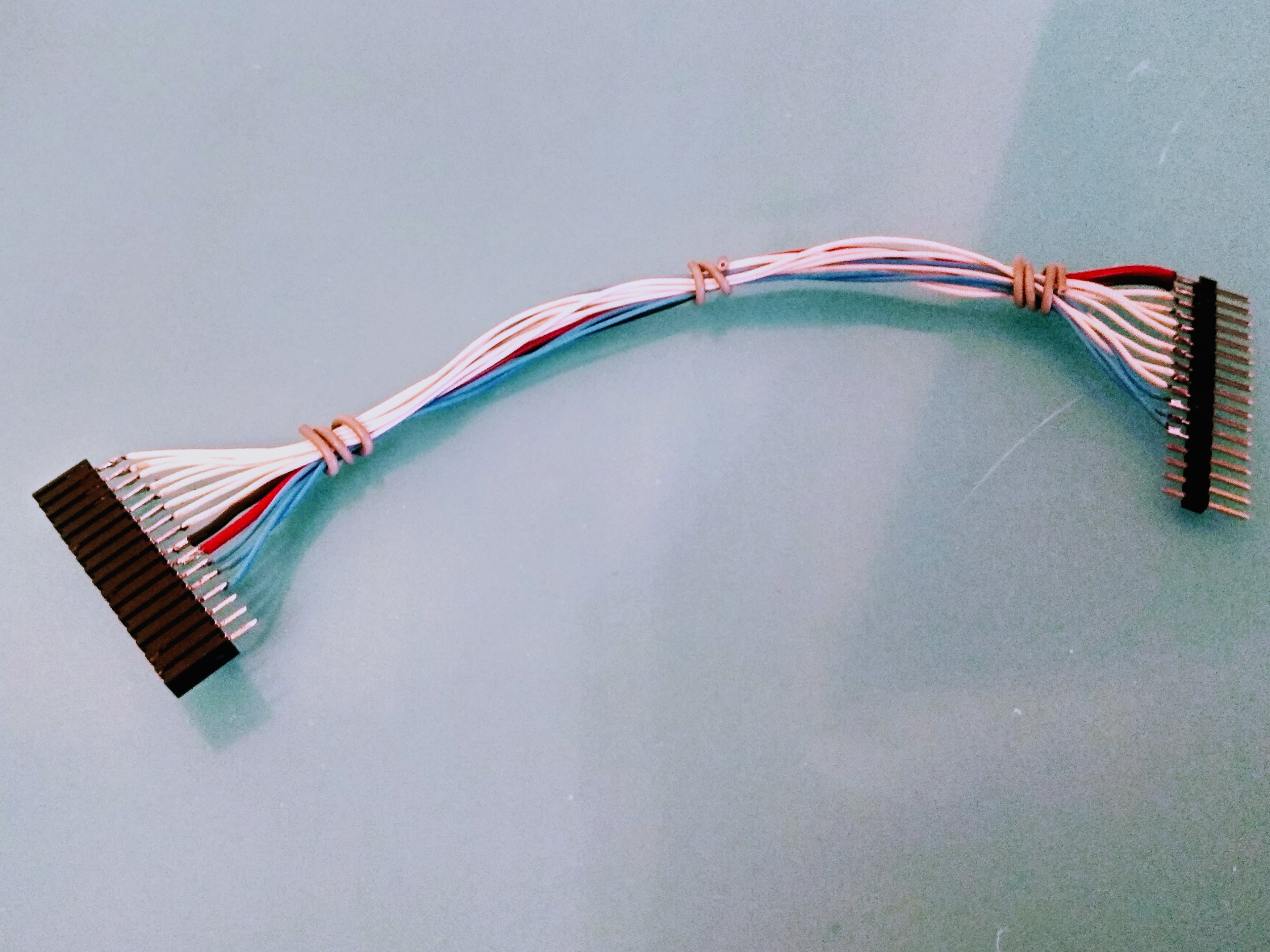
01/08/2019 at 18:09 • 0 commentsThe display and keyboard have to be connected to the CPU tower or it won't have any purpose other than looking pretty.
So I need to bring over the databus, control signals and power to the latches and the transceiver on the keypad/display unit. Initially I thought about just soldering cables directly onto the tower and then have a connector at the end that plugs into the display, but that didn't feel right.
Soldering a pinheader onto the databus is easy and fast enough even as the deadline is approaching quickly.
![]()
Then it was just a matter of making a short M/F cable...
![]()
-
Clock and Reset
01/07/2019 at 17:14 • 0 commentsI'm getting a bit stressed now, it's only a bit over 24 hours until the deadline and I haven't even tried the CPU yet.
One of the most important things needed to get it running is the Clock and a Reset unit.
So a cobbled together a small two-chip device with a 74HTC04 (hex inverter) and a 74HCT393 (dual 4-bit counters) for this.
Half of the '04 is a used for the Reset-button and driving the reset LED. The other half is a 7.37Mhz crystal oscillator which is the same frequency the RC2014 uses.
Since the wiring of the bus is a bit "unconventional" and also have a 1 Meg resistor between the individual lines I'm not fully convinced that I can run this at the 7 MHz clock frequency. So I added a 4 bit binary counter after the oscillator so I can select either 7.37 Mhz, 3.68 MHz, 1.84 MHz, 921 Khz or even a slow 460 KHz.
If I really wanted to go even slower I could hook up the second part of the counter) to gen all the way down to 28 KHz but I see no real reason for that. Then it would be more fun to have a 10 Hz clock rate to really get the LEDs blinking in a rate that's visible.

Clock and Reset unit 
Clock and Reset unit backside -
Blinky bus LEDs
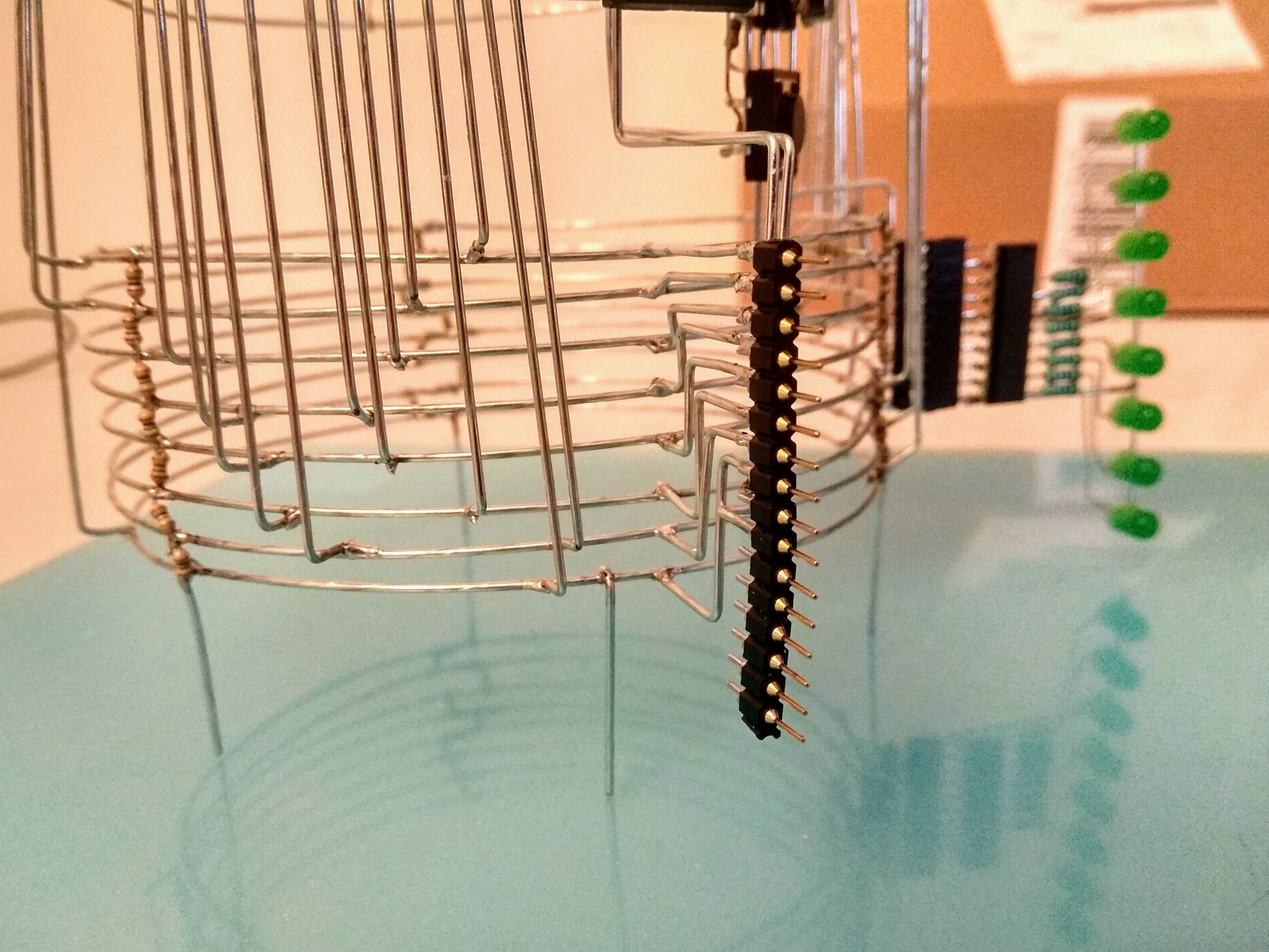
01/07/2019 at 16:44 • 0 commentsI decided to add some blinkenlights to the project so I tacked on a 10 pin header on the side of the databus rings (8 databits plus VCC/GND) and a 18 pin header on the side of the addresses rings.
For the databus I soldered up a female pinheaded directly to the inputs of a 74ACT245 octal transceiver and hooked up eight leds via resistors to it. Easy and straightforward soldering and looks not too shabby.
The addresses unit gave me a bit more grief. The A0..A7 from the pin header should be connected just straight over, but then there's the GND of the first '245 and pin 1 on the second that is not a part of the bus itself. So the connections between the second '245 and the pinheader is shifted two pins. And the spacing between the LEDs makes the routing of the resistors between the LEDs and the output of the '245s a bit awkward.
But I got it together in a semi-nice shape in the end at least.

Databus LEDs drive by a 74ACT245 
Address- and Databus LED modules 
Inserted in the headers on the CPU tower -
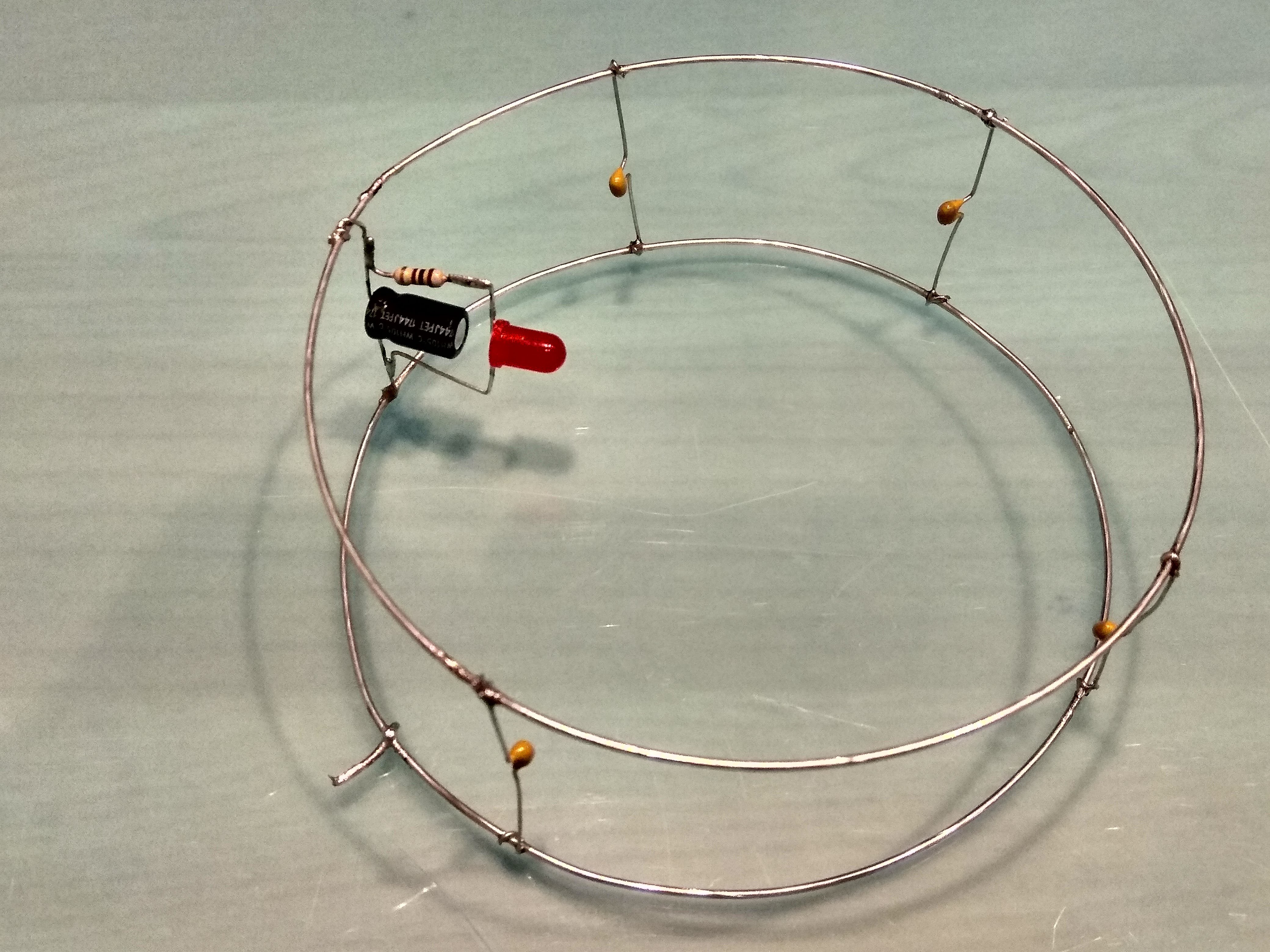
Power rings
01/05/2019 at 23:56 • 0 commentsFor the power-bus I made two a bit smaller rings that will be put inside the other rings, behind the ICs. The spacing between the GND and VCC rings are 1.4" so they can end up siting exactly behind pin 14 and pin 28 of the memory ICs.
They are helt together with a couple of 100nF caps and a 470uF bulk cap.
I also added a power LED in the ring, debating with myself if I should use a blue (kinda cool but utterly crap looking for anything retro), so I selected a non-clear red LED.
![]()
-
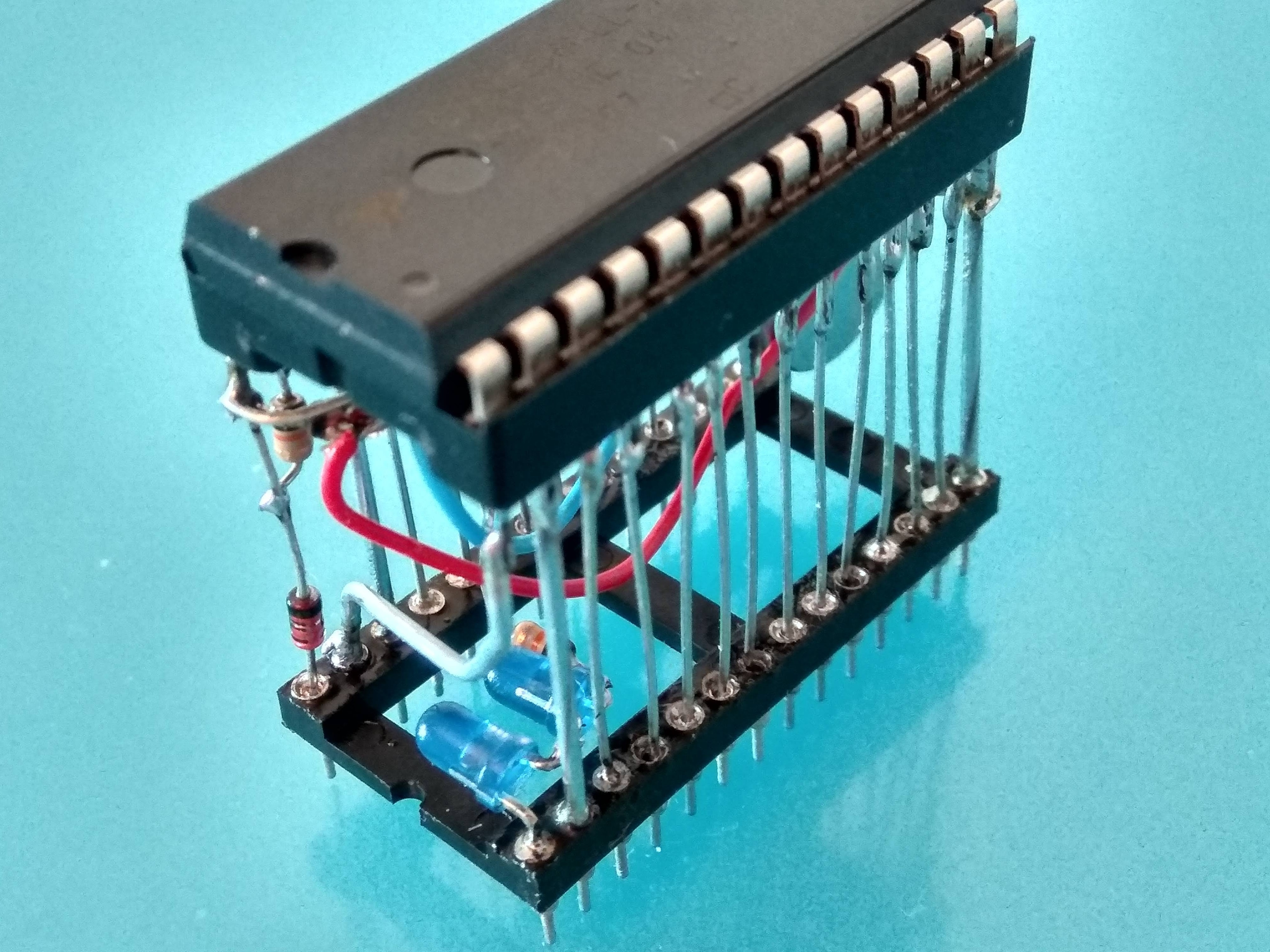
The PROM that wasn't EE nor UV
01/03/2019 at 12:39 • 1 commentI thought it was a real 27C512 UV EPROM I had in one of my junk boxes, but after peeling off the sticker on top of it it turned out to just be a OTP PROM. I'm definitely not confident that I'll be able to make the firmware 100% working at the first try so I had to come up with a solution for this.
I have some extra SRAMS laying around so I used the project at https://hackaday.io/project/8109-sram-as-replacement-for-eprom as a basis for my battery backed SRAM that emulates a 27C256 EPROM.Since I didn't have any super capacitors and self-discharge of the 2200uF I already had at hand indicated that they would be flat inside 24 hours I decided to use a CR2032 coin cell battery as the backup power for the RAM.
The next setback was that I couldn't find a battery holder in my drawers, I tried to solder wires directly onto it. I've seen it be done, but I couldn't get the solder to wet the battery casing even if I used a fat tip on the iron and aggressive flux. I even tried to lightly sand the surface down a bit before soldering - but no joy.
I ended up soldering the wires to two neodymium magnets instead. Of course soldering on a magnet is not a good idea, since one easily reaches the Curie temperature which will kill the magnet permanently (pun intended) dead. But by soldering really fast to an edge while keeping the bulk of the magnet cool by holding it with tweezers I was able to solder wires to them while still having enough magnetic force left in them to be able to stick fairly good to the battery.
")
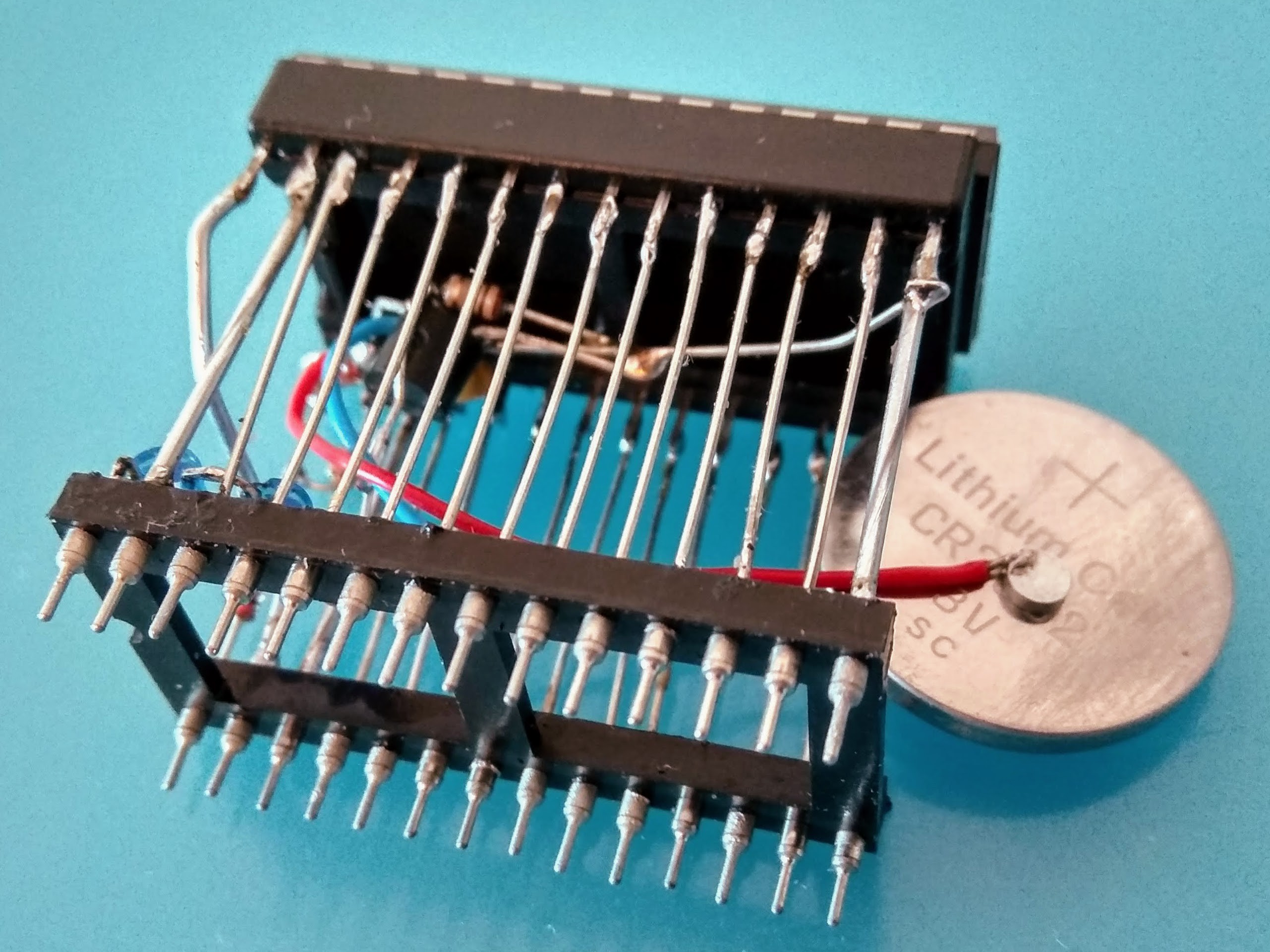
(The blue magnet should of course be stuck on the bottom of the battery) The schematics for my version of the battery-backed SRAM looks like this. Compared to the super-capacitor variant I've just added a diode between the battery and the SRAM to keep the external VCC trying to "recharge" it - I'm sure the battery would be mightily upset by that and express its anger in some fireworks and smoke sooner or later ;-)

Schematics of the battery backed SRAM emulating a 27C256 After soldering it up it looks like this and can be programmed using my TL866 - I just have to remember turning off the Chip-ID function of the software since it actually puts out 12 volts at A9 - the SRAM probably won't survive that. I probably should solder in a clamping diode between A9 and VCC on the SRAM to keep it safe(er) from being electrocuted into oblivion by my forgetfulness.
![]()
![]()
And yes - I did wrap some tape around the battery before tucking it into between the sockets....
-
Tower of CPU
12/29/2018 at 16:06 • 0 commentsBending 24 wires and cutting them to the right lengths was easy using a template that I made in Eagle .

40 pin CPU socket with cut and soldered address&data busses I'll handle the remaining connections later, for now I'm happy to just get most of the wires done to get a rigid frame to work on.
Soldering this "spider" onto the cylinder was a bit scary, it felt like I almost broke off some of the legs on the IC socket. I really should have used a socket with higher quality...
But it ended up in once piece - and not looking so horrible that I'd just abandon the project. :-)

The CPU socket in place on the frame
So far so good, now I only need to add two 28-pin and one 24-pin sockets as well. I'm not 100% convinced that I can fit them there so I might have to skip the UART and only go for the RAM and ROM. -
More rings and tower
12/29/2018 at 11:03 • 0 commentsNow when the UI part is done I spent some time to get cylinder/tower ready to start hook up the CPU and memories to it.
The sixteen rings was easy to make with the new jig I 3d-printed to keep the rings steady while soldering together the ends of them. (The jig reminds me of something - maybe the Quake logo?)

The 16 address bus rings and the jig Now that I got some experience from soldering the smaller databus it was rather easy and fast to solder up these 16 into a decently looking cylinder.
Then I (temporarily) patched the two separate cylinders together with three wires to make some distance between the buses where the ICs will be soldered.

The slightly leaning tower of Pisa - I.E the data & address busses -
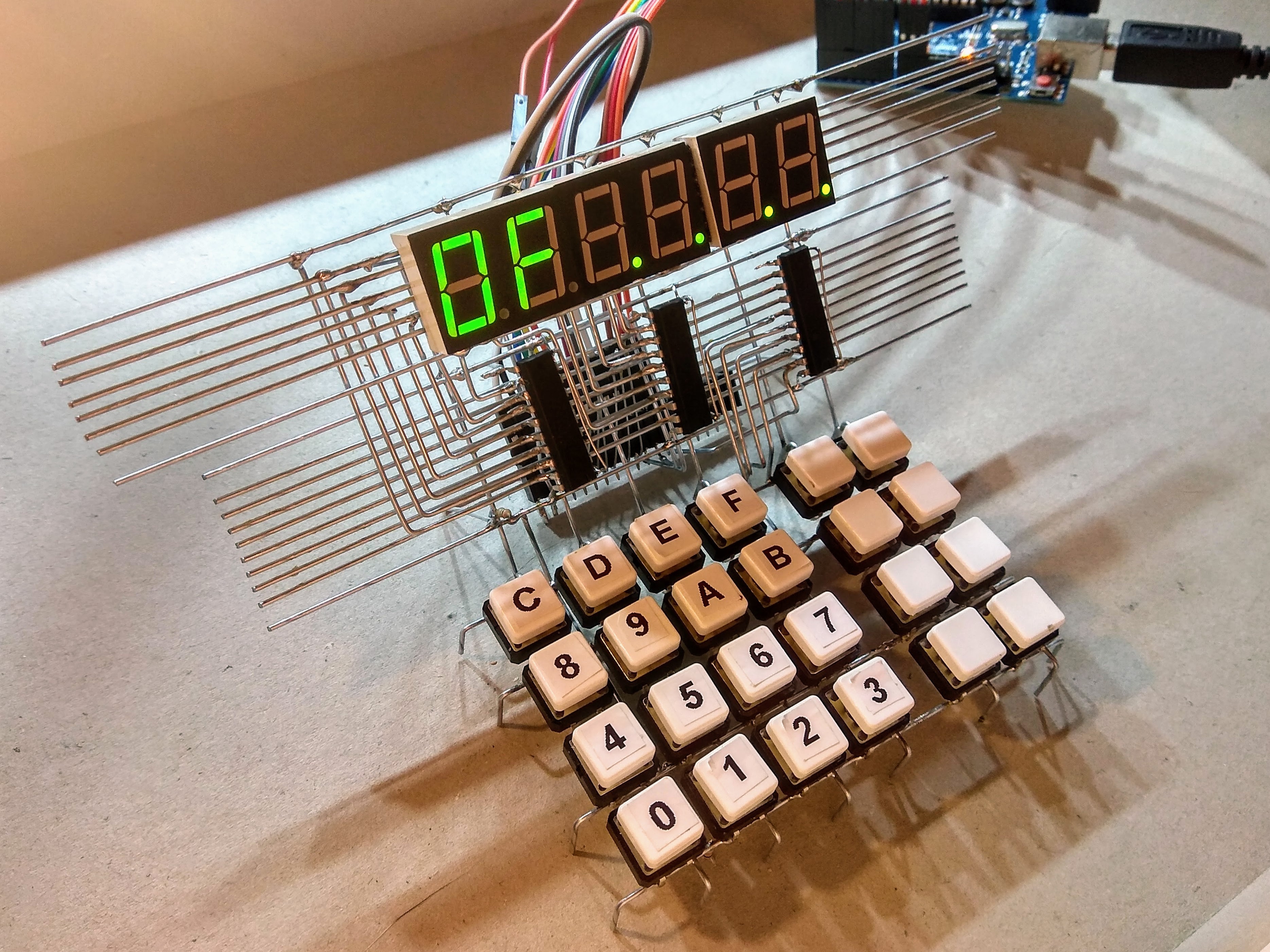
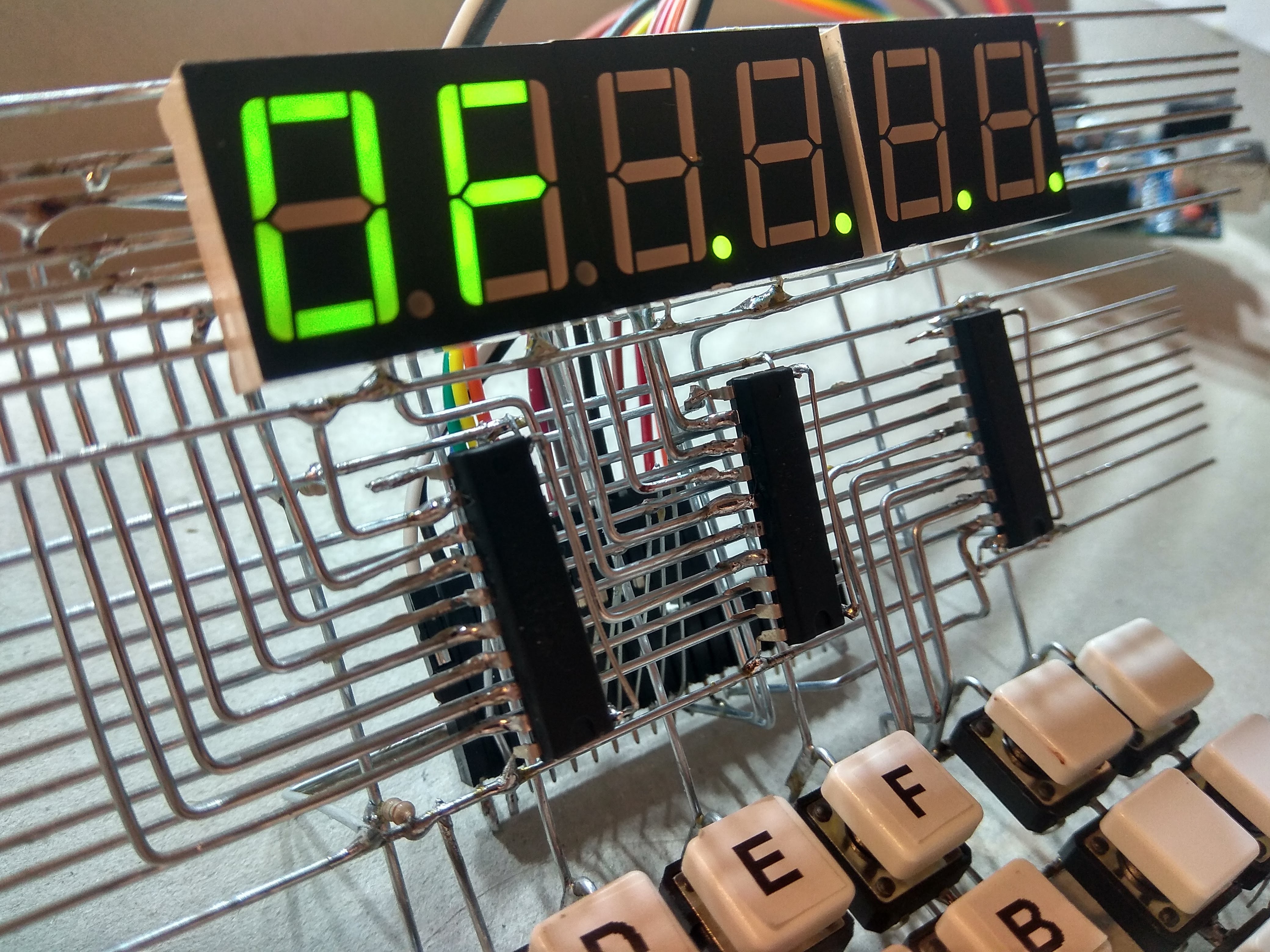
User interface finished
12/28/2018 at 23:51 • 0 commentsChristmas slowed down the progress of this project a bit, but today I connected up the latch-"board" to the display&keypad module.
It was bit hard to solder up, but I think it ended up in a not too bad shape - there are quite a lot of connections between the two units so some creative routing was necessary.
I also had to forego my initial plan to have the displays and segments in an easy ascending bit order, they ended up a bit scrambled but that is not a big issue since it's easy to fix that in the firmware that refreshes the display.
At the backside of this module I added a 20 pin female 0.1" header to connect to the CPU module with some flexible wires. Having them soldered permanently attached with AWG 18 wires would not be fun during building and testing.
![]()
I hooked the databus and three control signals up to an Arduino and wrote a short program to test the displays and the keypad. It worked just fine after I added pull-ups between the keypad and the 74245 transceiver. I had overlooked that floating inputs of the logic family of the 245 I was using did not consistently read high as the old LS-series would do.
![]()
wirez80
Z80 machine with a hex keypad and 7-segment displays built on a cylindrical wireframe


")