Plasmode
-
Stage 3, Installing CP/M
03/03/2019 at 13:18 • 0 commentsTo support CF disk and CP/M, the ZMon64 monitor has several additional commands. The monitor is tailored for a particular CP/M configuration which is four 8-meg disks as drive A/B/C/D. The following is the disk parameter of each drive:
Drive A:
1024 sectors per track,
4096 bytes per block ,
track offset of 1,
512 directory entries
Drive B/C/D:
1024 sectors per track,
4096 bytes per block,
track offset of 0x40 from previous drive,
512 directory entries.To format a new CF disk for CP/M, the directory area of each drive must be filled with 0xE5. The 'x' command of ZMon64 formats the specified drive. The command to format drive A, B, C, D are retrospectively:
xA
xB
xC
xD
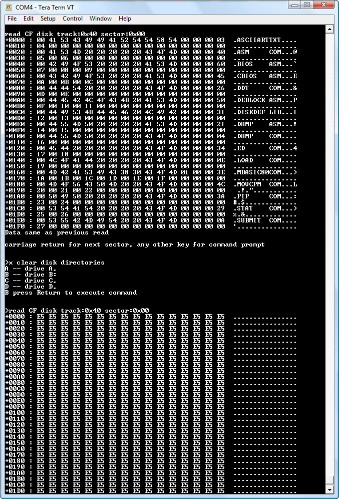
Please note the drive letter must be in upper case.ZMon64 also has a command to read a CF sector. The command is 'r' followed by track number and sector number in hexadecimal. Based on the disk parameters, drive A's directory starts from track 01, sector 00, drive B's directories starts from track 0x40, sector 0x00, drive C's directories starts from track 0x80, sector 0x00 and drive D directories starts from track 0xC0, sector 0x00. Each drive has 512 directory entries, so that takes 32 sectors. Picture below is a screen shot of a console session where directory of drive B is displayed with 'r 40 00' command. Drive B is formatted with 'xB' command, and directory displayed again which show all '0xE5'
![]()
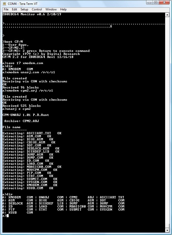
ZMon64 has two more commands related to CP/M: 'c' command to copy files into CF or RAM; and 'b' command to boot up a file. For CP/M 2, the copy command is 'c2' and the boot CP/M 2 command is 'b2'. Before executing the 'c2' command, the CP/M2 CCP/BDOS/BIOS must be first loaded in memory so 'c2' command can save it to designated location on a CF drive. Both 'b2' command and CP/M2 warm boot access the designated location for CCP/BDOS/BIOS.
I'm not going to describe the process of creating BIOS for CP/M2. Having a working CCP/BDOS/BIOS that is installed in a formatted CF disk with 'c2' command, the next step is to transfer CP/M executable files into the newly formatted CF disk. The file transfer program is XMODEM, so load XMODEM.HEX first then boot up CP/M2 with 'b2' command, then type:
save 17 xmodem.com
This will save the XMODEM.HEX image in RAM as a CP/M file called 'xmodem.com'. The first CP/M file is now created on the CF disk. Use xmodem to transfer the rest of files to the CF disk with the command:
xmodem filename /r/c/z1
Instead of xmodem each individual files, it is easier to compress a collection of files, transfer it over, and decompress in CP/M. There are many such compress/decompress programs, the one I used is arj.exe/unarj.com. CP/M2 executable are compressed with arj.exe; I first xmodem the unarj.com and compressed CP/M2 executable; then decompress it with unarj.com:
unarj e cpm2
Here is a screen shot of the series of operation to create CP/M files on a new CF disk.
![]()
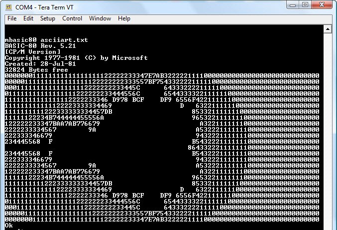
WIth CP/M2 installed, one quick benchmark to run is ASCIIART.TXT which should take 52 seconds to execute on a 22MHz Z80. At the CP/M prompt, type:
mbasic80 asciiart.txt
The following should be displayed.
![]()
-
Stage 3, CP/M-ready Hardware
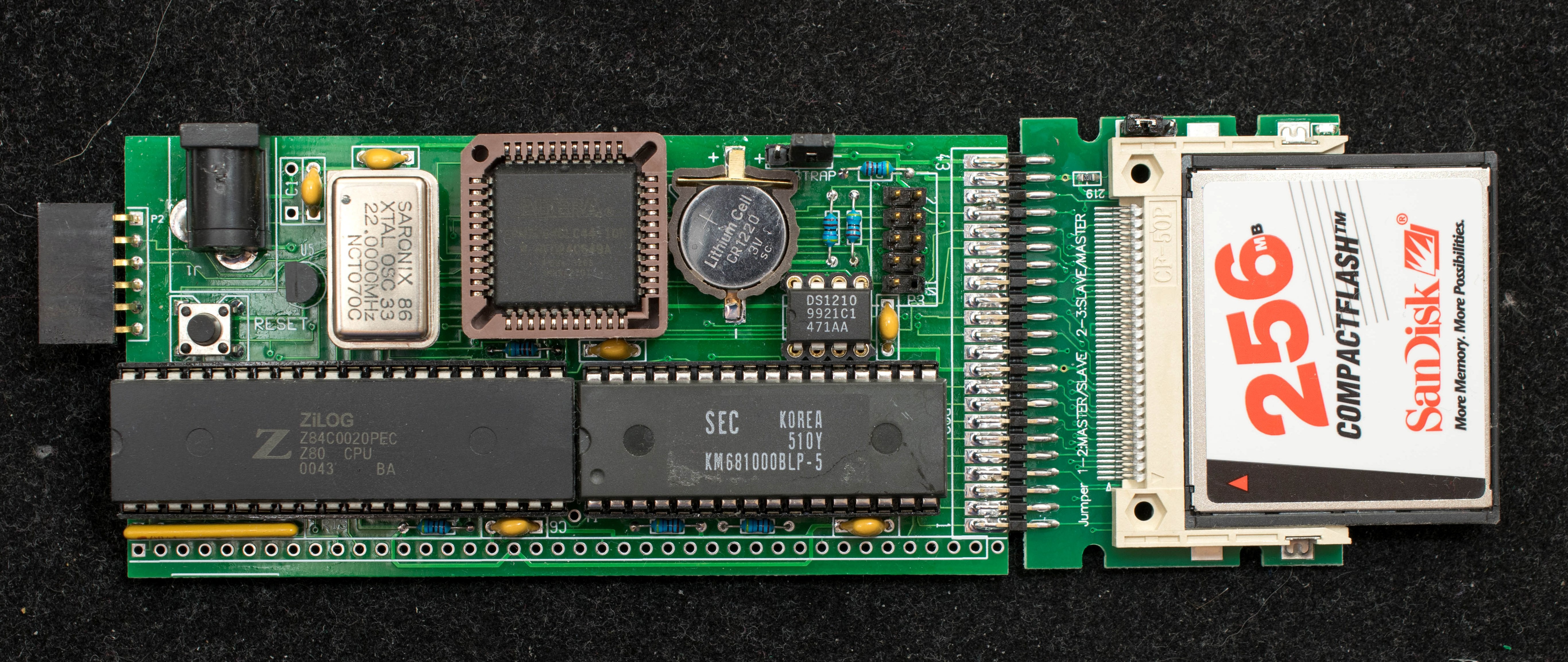
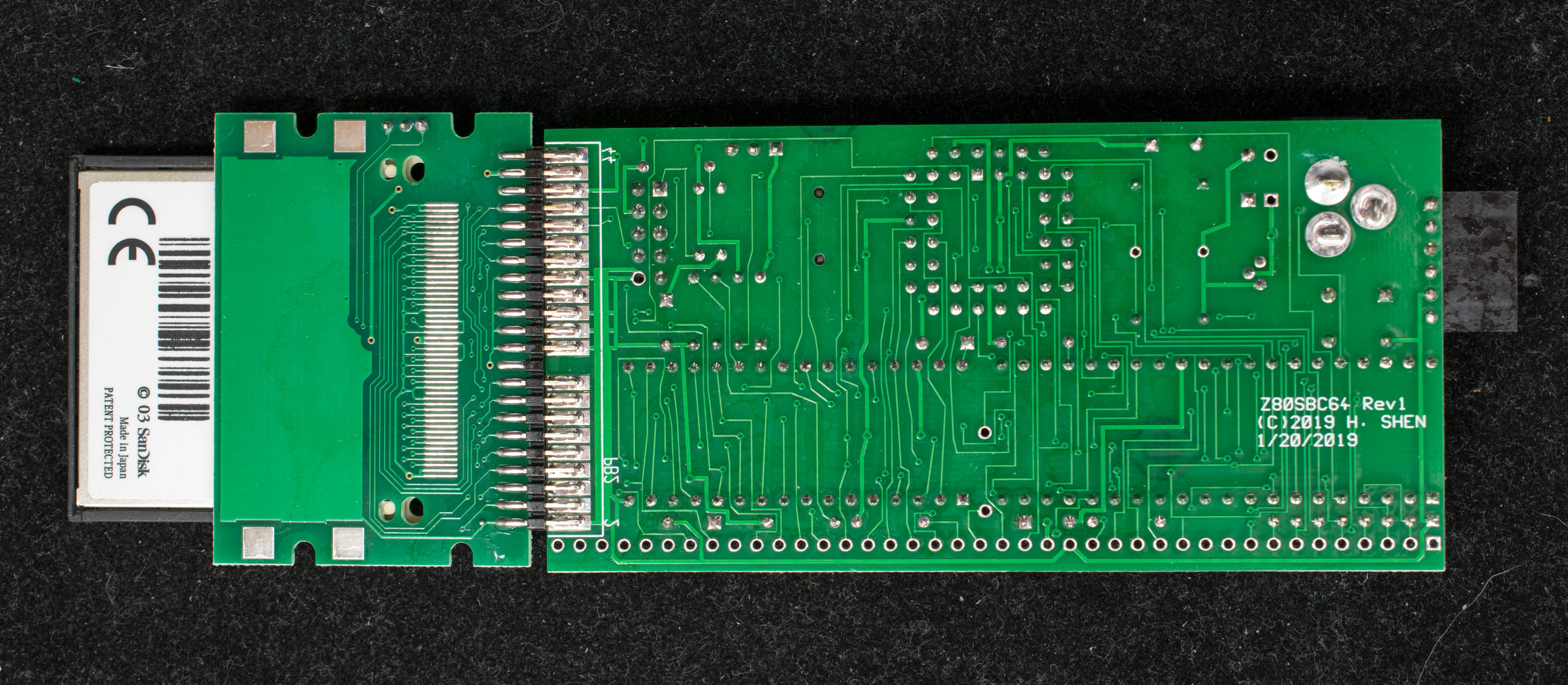
03/01/2019 at 14:59 • 0 commentsWhile it is possible to have CP/M reside in system that has only non-volatile RAM, Most CP/M system have a mass storage device in form of floppy disk, hard disk, and/or flash disk. The Z80SBC64 is designed with a compact flash disk interface. The hardware addition is simple, just solder a IDE44 adapter to the CF interface and Voila, we now have the CP/M capability.
![]()
![]()
CP/M software, however, is quite a bit more involved. Fortunately a system integration guide for porting CP/M to specific hardware is still readily available from Internet. http://cpm.z80.de/ is a well-know repository of CP/M for Z80 and other processors. It is not my intention to provide a tutorial on porting CP/M to Z80, but I do want to describe certain CP/M related functions specific to Z80SBC64 in next project.
-
Stage 2 Hardware, Non-volatile RAM
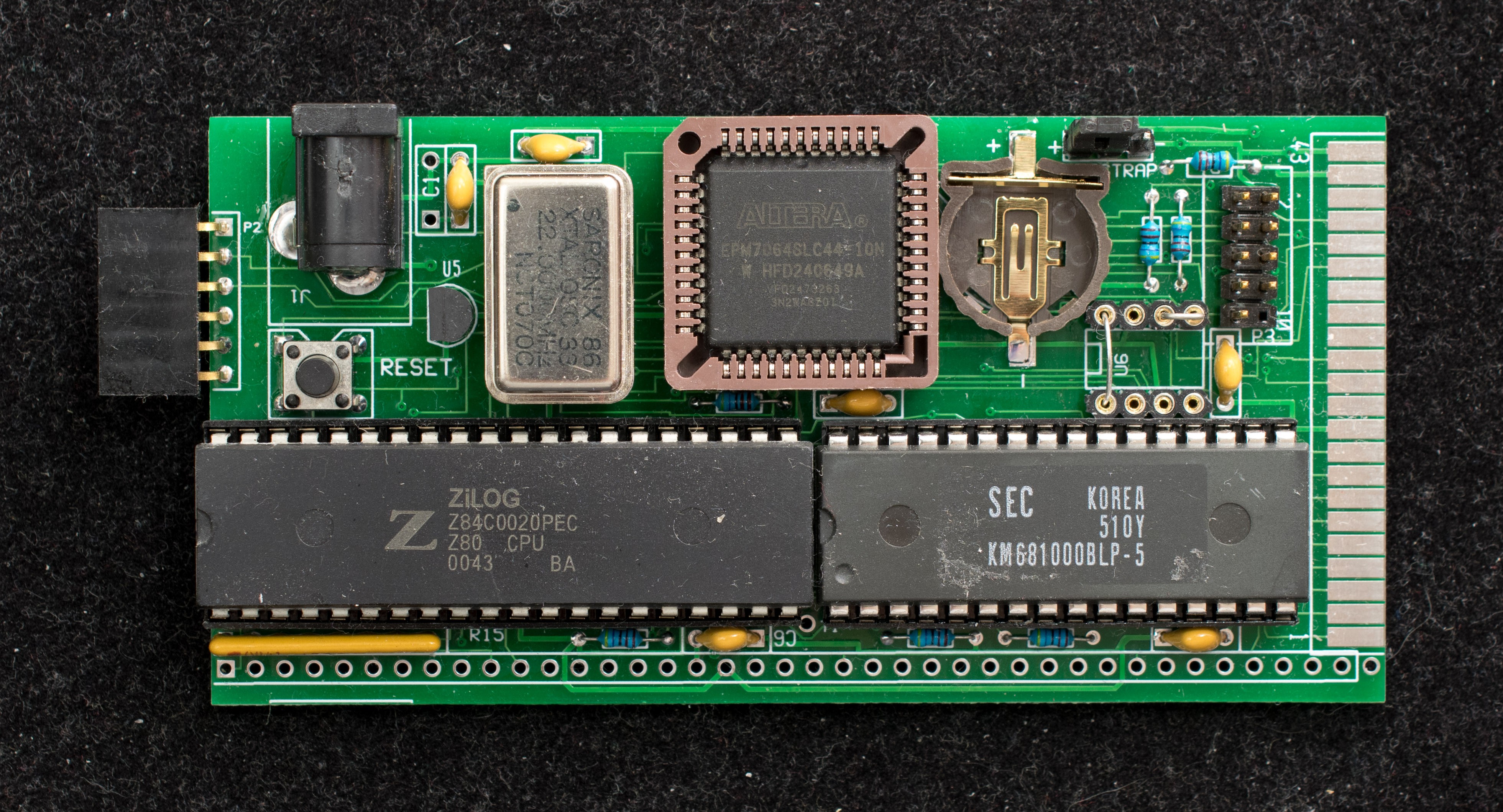
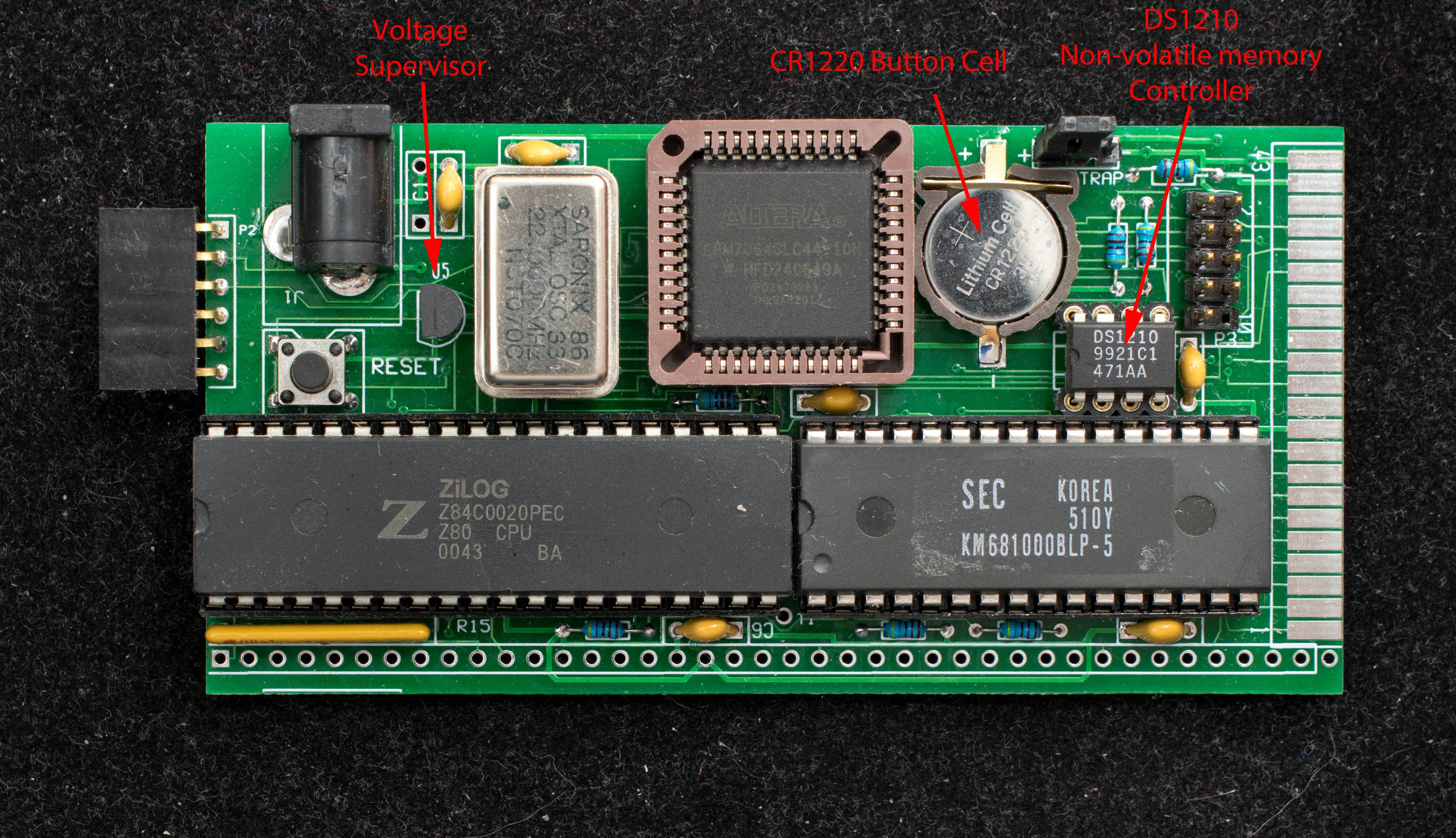
02/28/2019 at 17:12 • 0 commentsWhile loading a small bootstrap code serially is fairly easy and quick, but as the application software get bigger and numerous, the process of loading several software every power cycle or reset become tedious. Fortunately the RAM has extremely low power consumption in standby voltage of 3V or less, so its content can be retained for a year or more with a button cell battery and non volatile memory controller. In stage 2 of the hardware assembly, we'll add the button cell battery and install the non-volatile memory controller.
![]()
The two jumpers in U6 are removed and replaced with DS1210. A CR1220 3V Lithium cell is inserted in the battery holder as shown. While it is not absolutely required, the voltage supervisor is also installed in this stage so we don't have to press reset button for every power cycle.
![]()
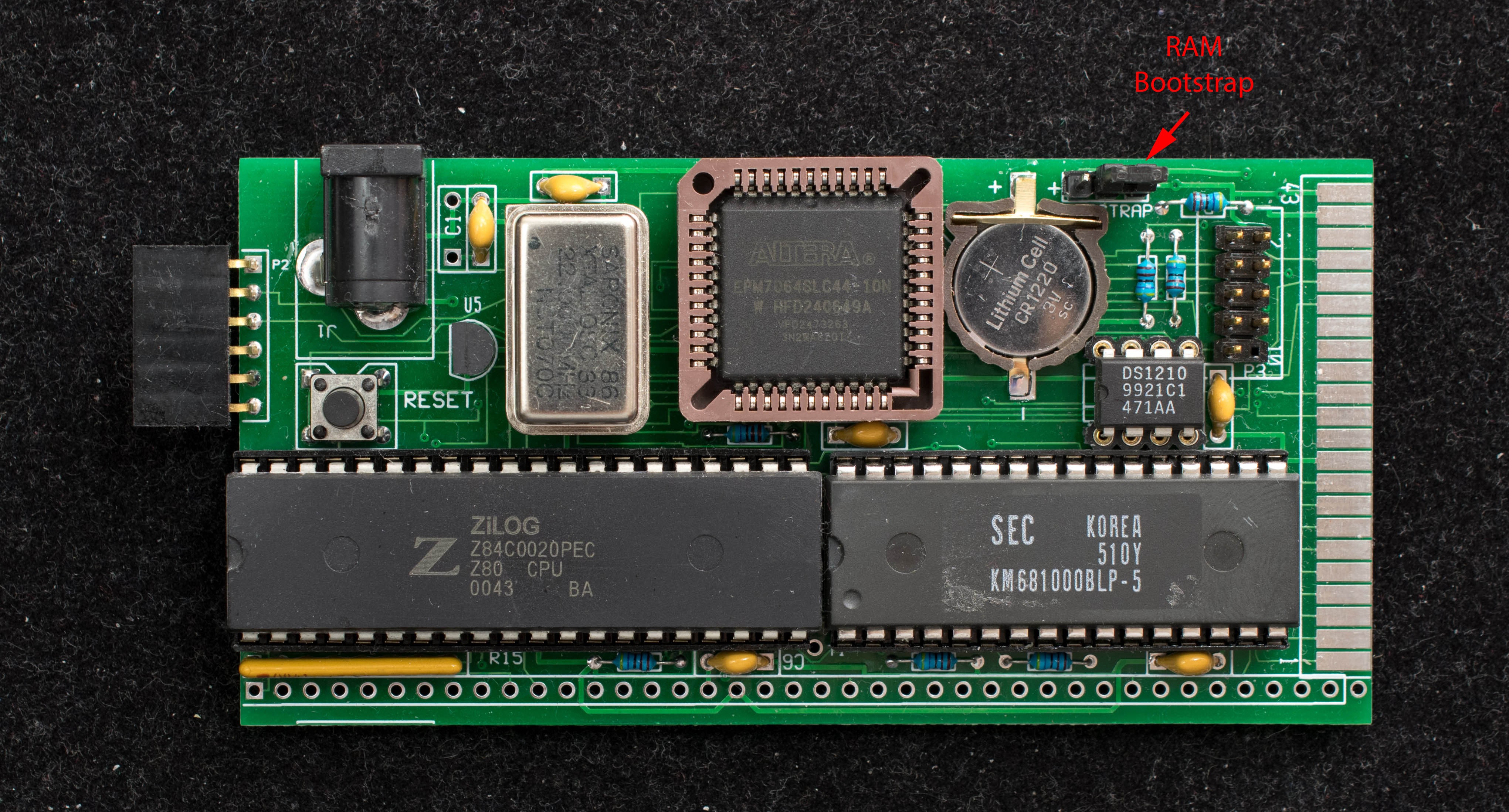
Just because the RAM's content is retained between power cycles, we are not yet safe from having to load code over and over again. This is because application codes like CP/M takes over the entire memory space and write into page 0 (0x0 to 0xFF) of the RAM. To prevent the bootstrap code from being overwritten, we need to place it in a banked memory that's accessible at reset, but can be switched out and replaced with another bank. As explained in the Theory of Operation, the 128KB RAM is splitted into four 32KB banks with bank 2 as the common memory always at the top 32KB and bank 3 located at lower 32KB at reset. A bank select register can place bank 0 or bank 1 at lower 32KB under software control. Z80Monitor has a command 'c0' that copies itself from 0xB000-0xBFFF into 0x0-0xFFF of bank 3 and switches out bank 3 and switch in bank 0 in its place. So with the 'c0' command, Z80Mon make itself boot-able and hidden from other applications. Other applications such as CP/M will have unfetter access to the entire Z80 memory space, but power cycle or reset will enable the bank 3 where Z80Mon is located and boot up with Z80Mon.
We can zero out the entire memory (other than ZMon) with the 'z' command, but it will still boot up with reset or power cycling. With bootstrap code safely protected from application software, we can now move the jumper to RAM bootstrap position and power up to Z80Monitor every power cycle or reset.
![]()
Bank 3 has 32KB of storage, but only 4K is reserved for Z80Mon. The remaining space can be used to store other application, such as SCMonitor. This is what 'c1' command does. It copies whatever program from 0x0 to 0x3FFF to bank 3 and 'b1' command restore the content of 0x0-0x3FFF from bank 3 and start execution from 0x0. So 'c1' command saves SCMonitor, and 'b1' command boot up SCMonitor. Bank 3 is effectively a non-volatile memory, but one that can be easily written.
With the serial bootstrap capability and banked nonvolatile RAM, we now have a Z80 computer that can be reprogrammed from scratch at will, but yet retain its characteristics over reset and power cycling. We are ready for stage 3 and tackle CP/M!
-
Running software on the minimal Z80SBC64
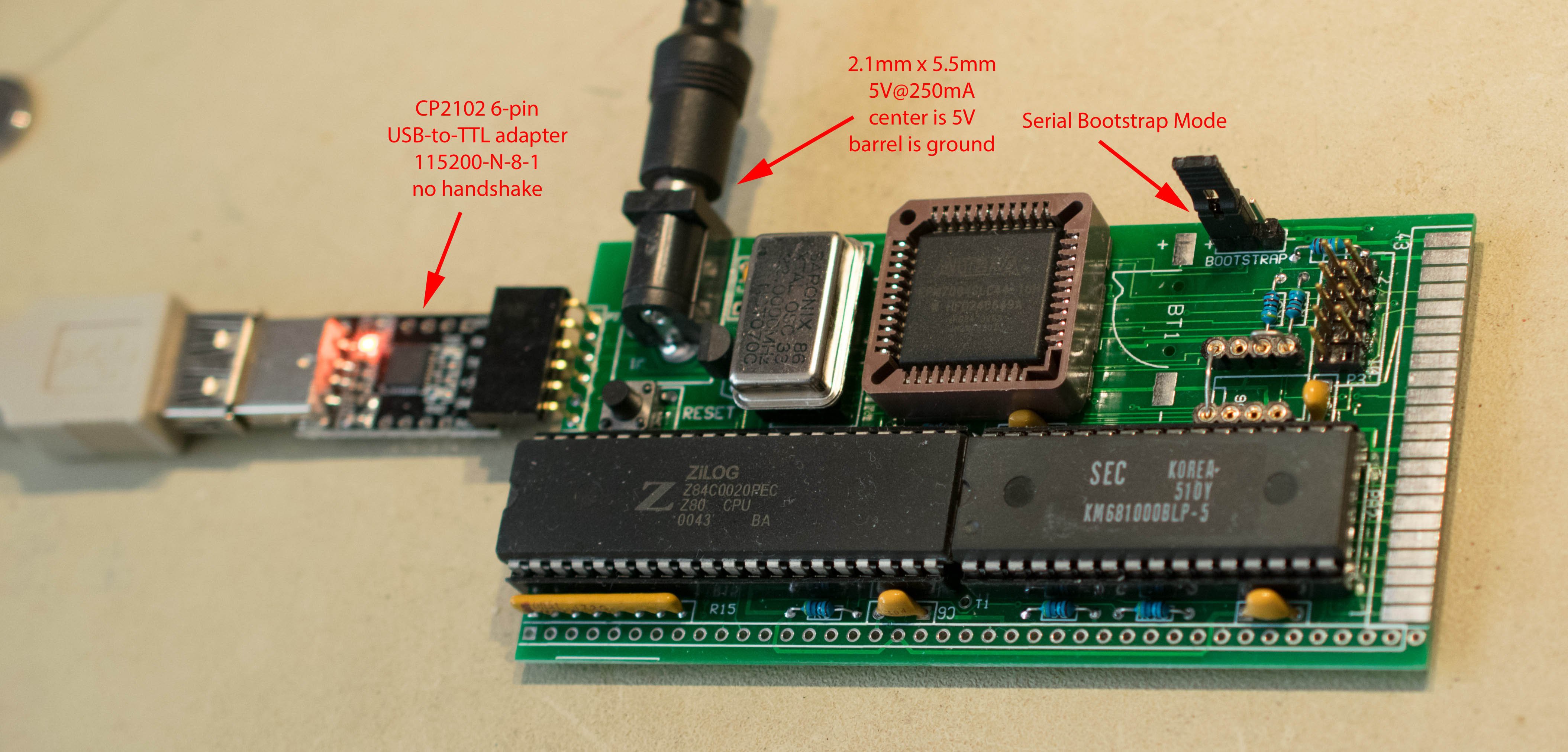
02/17/2019 at 16:22 • 0 commentsI'm ready to apply power to the minimal Z80SBC64 hardware. It needs 5V, 250mA power via 2.1mm x 5.5mm power plug, center is 5V, barrel is ground. The serial port is wired to accept a CP2102 6-pin USB serial adapter. Terminal software is TeraTerm set to 115200-N-8-1, no handshake.
![]()
Power up!
The current consumption should be around 100mA, Z80 is tri-stated waiting for incoming serial data. The first file to send is Z80SBCLD.BIN. This is a 255-byte binary file that is a simple Intel Hex file loader. Be sure to check the 'binary' option box of the "Send file" menu in TeraTerm. The Z80SBC64 should respond with:
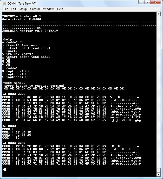
Z80SBC64 Loader v0.3
Auto start at 0xB400This means Z80 is alive and executing the Z80SBCLD program, current consumption should goes up to 140mA. The bootstrap file loader is waiting for 2nd file and will start execution from 0xB400 upon completion of the 2nd file load. Be sure to un-check the 'binary' option box because all subsequent files will be Intel HEX files. The 2nd file to load is ZMON64.HEX. This is a monitor/debugger for Z80SBC64. After the 2nd file is loaded, it will start execution at the entry address of 0xB400 and sign on. A 'h' display the help menu:
>help
G <addr> CR
R <track> <sector>
D <start addr> <end addr>
I <port>
O <value> <port>
L <start addr> <end addr>
Z CR
F CR
T CR
E <addr>
X <options> CR
B <options> CR
C <options> CRThis monitor can display, modify memory, read/write I/O ports, zero or fill memory, load Intel HEX files and test memory. There are other functions but working only when a compact flash disk is installed later on. A 't' command will test memory and print 'OK' if memory is OK. Any input keystroke will abort the memory test. Picture below shows a monitor session.
![]()
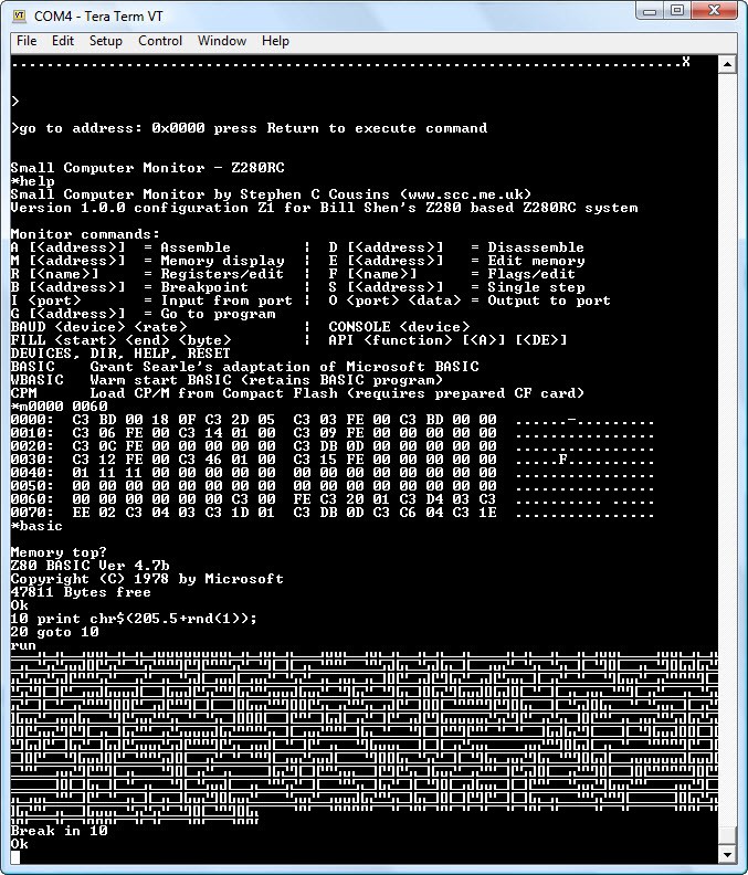
While this is interesting, there is a more sophisticated monitor, SCMonitor, that also runs on Z80SBC64. SCMonitor is written by Steve Cousin and more information can be found on his website. To load SCMonitor, send SCMon.hex to Z80SBC64, when file load is completed, type 'g0000' to start SCMonitor. Refer to Steve Cousin's SCMonitor document for operating instruction. Included in SCMonitor is BASIC 4.7b. You can enter the BASIC program by typing 'basic'. Picture below shows a short session with SCMonitor.
![]()
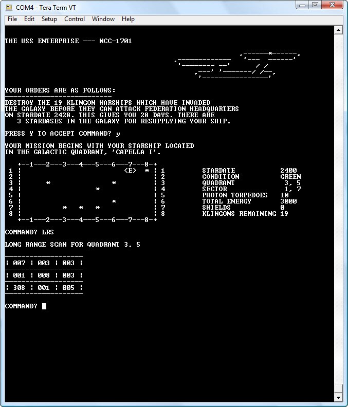
This is all well and good, but where is the GAMES? Well, I'm glad you asked because StarTrek runs in BASIC 4.7b. Instead of cut-and-past the long StarTrek BASIC program into SCMonitor, there is an Intel Hex file of SCMonitor already with StarTrek program loaded. So load up SCMonitor_Startrek and "Beam me up, Scotty"!!!
![]()
-
Z80SBC64 Theory of Operation
02/16/2019 at 16:41 • 0 commentsZ80SBC64 has two modes of operation as determined by the Bootstrap jumper at power up (see the last picture of the previous project for location of bootstrap jumper).
Serial Bootstrap
At power up Z80 processor is tri-stated waiting for 255 bytes of instruction is be uploaded to the serial port (115200 baud, N81, no handshake) which is copied to memory starting from location 0x0. When the 255th byte of data is received and copied to memory, the CPLD state machine release Z80 to run from location 0x0. The 255-byte code can be any software such as hardware diagnostic, but is normally a simple file loader to load more sophisticated application software. In this stage, it is a simple Intel Hex loader, Z80SBCLD.BIN that loads a monitor/debugger and executes it at the completion of file load.
RAM Bootstrap
This is normal mode of operation. At power up, Z80 fetches program from physical location 0 which contains the bootstrap monitor. The bootstrap monitor write-protect physical page 0 where bootstrap monitor resides. It then makes a copy of itself to 0xB000-0xBFFF and jump to it. Lastly the physical page 0 is replaced with logical page 0 which mapped to different physical page. This way the physical page 0 containing the bootstrap monitor is write protected and moved out of way. The application program will have unfettered access to all 64K space of the target processor.
Memory Map
Z80SBC64 has 128KB of RAM which is divided into 4 banks of 32KB each. At any time only 2 banks (64KB) are accessible by Z80. Bank 1 is always at the upper 32KB memory (0x8000-0xFFFF), it is the common memory that can not be switched out. The lower 32KB can be switched between bank 0, 2, and 3 by writing 0x0, 0x2, and 0x3, respectively, to the bank register. At reset the lower 32KB is always mapped to bank 3. Bank 3 contains the bootstrap monitor code that copies itself to upper 32KB and switch bank 0 into the lower 32KB, thus protect the content of bank 3 from other programs.I/O Map
Bank Register is located at I/O space 0x1F. It is a write-only register, a read will get random value. Only the least significant 2 bits of the Bank Register are used, the upper 6 bits are "don't care". At reset the content of bank register is set to 0x3 which maps bank 3 to the lower 32KB. Bank 3 is reserved for the bootstrap monitor and system software. Writing 0x2 will map bank 2 to the lower 32KB of memory space. Bank 2 is normally used by CP/M 3. Writing 0x0 will map bank 0 to the lower 32KB of the memory. Bank 0 is the default bank after the bootstrap monitor completes the booting process.Compact flash is located at I/O space 0x10-0x17.
0x10 CF Data Register
0x11 CF Error Register (read), Feature Register (write)
0x12 CF Sector Count Register
0x13 LBA Low, LBA(7:0)
0x14 LBA Mid, LBA(15:8)
0x15 LBA High, LBA(23:16)
0x16 Device Register, LBA(27:24)
0x17 CF Status (read) and Command (write) RegisterSerial port is located at I/O space 0xF8-0xF9.
0xF8 Serial Status Register
bit 0 is RxReady flag. bit 0 is high when receive data is ready. cleared to zero when the received data is read.
0xF9 Serial Transmit (write) and Receive (read) register. When write to 0xF9, TX pin of the CPLD is equal to the value of d(0) (bit 0) of the data. d(7:1) are "don't care". The serial port has no interrupt capability and no handshake. It is hardwired to 8 data bit, 1 stop bit and no parity. The baud rate is CPU clock /192. e.g., 22.1184MHz CPU clock results in 115200 serial clock. -
Stage 1 Hardware, Building A Minimal Z80 Computer
02/10/2019 at 04:47 • 0 commentsIn the first stage we'll build a very simple yet functioning Z80 computer with just 4 integrated circuits, plus resistors, capacitors and hardware. The bill of materials is included in the Files Section. In stage 1 the following items will be assembled:
Part Name Source U1 Z84C0020PEG Mouser 692-Z84C0020PEG U2 EPM7064SLC44 UTSource U3 128Kx8 Static RAM Mouser 913-AS6C1008-55PCN U4 22MHz oscillator R15 4.7K 8-pin SIP Bus Jameco 1970367 R1-4, R8-9, R16 4.7K, 1/8W C3-8 0.1uF bypass S1 Push button SPST Jameco 149948 J1 2.1mm x 5.5mm Power
JackJameco 101178 T34 3-pin header P2 1x6 right angle female
headerP3 2x5 header The pc board artwork is included in the FIles Section, so is the schematic of Z80SBC64 and the Altera EPM7064 programming file.
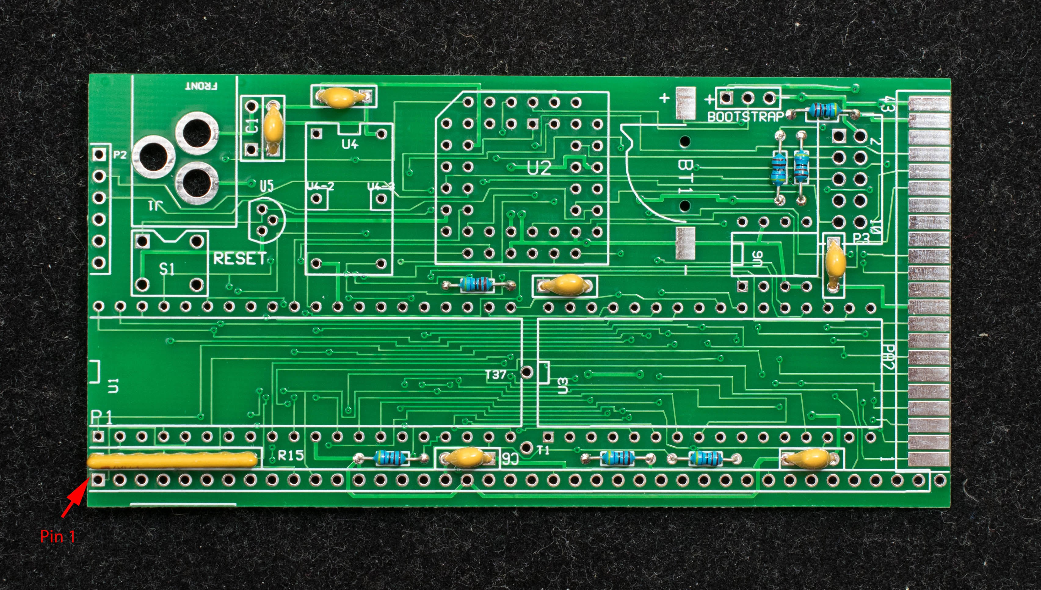
Here are step-by-step pictorial assembly guides for building a minimal Z80 computer. The order of assembly is based on the height of the components, the lowest components are soldered down first and the tallest last. In the first picture, all resistors (4.7K), bypass capacitor (0.1uF), and SIP resistor (4.7K BUS) are soldered down. Orientation of SIP resistor is important, pin 1 is marked with a black bar and oriented where the red arrow is pointed.
![]()
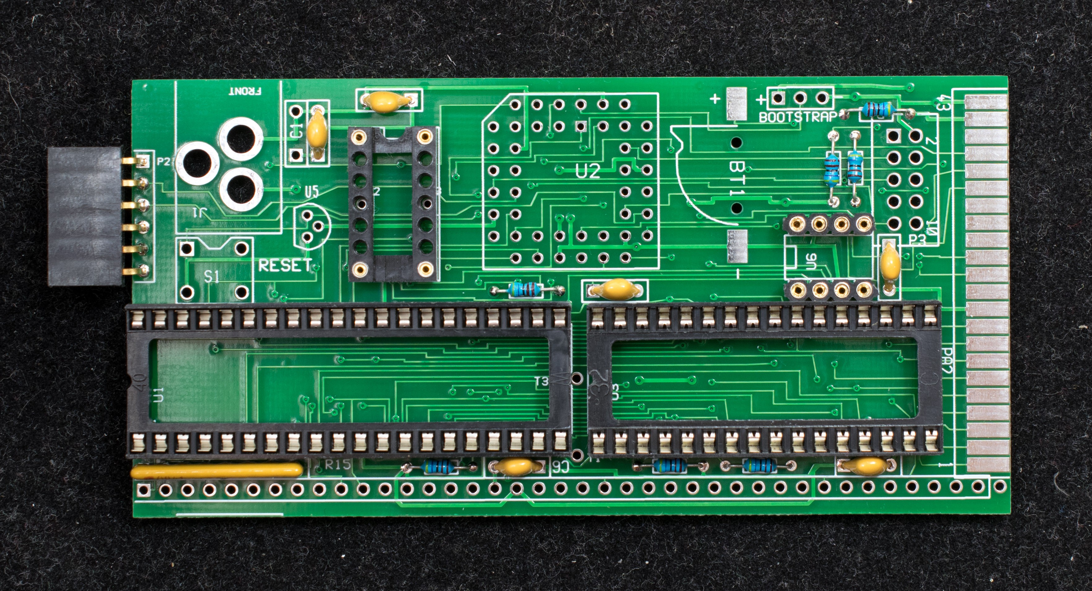
In the second picture, the IC sockets are installed as well as the 1x6 serial port header.
![]()
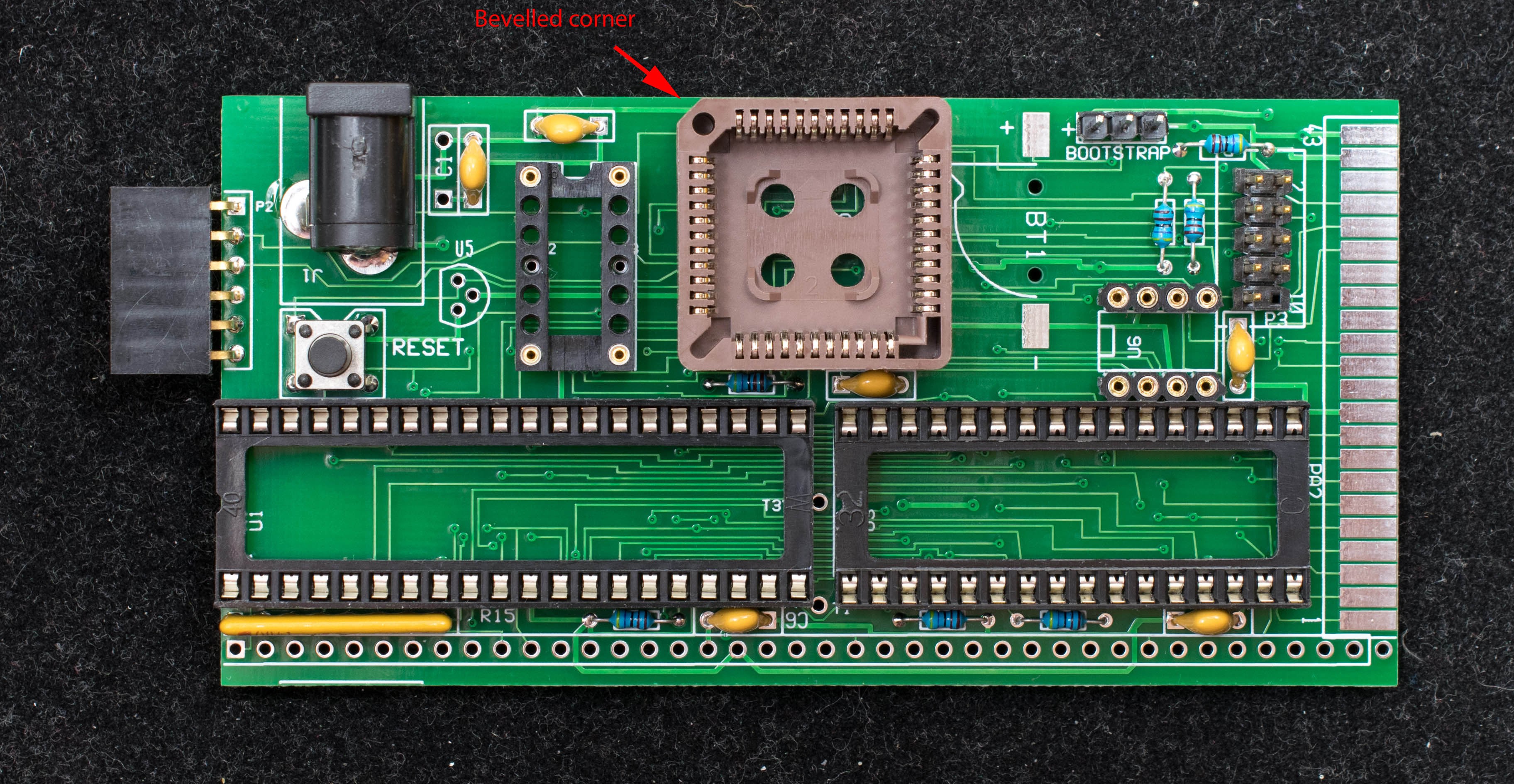
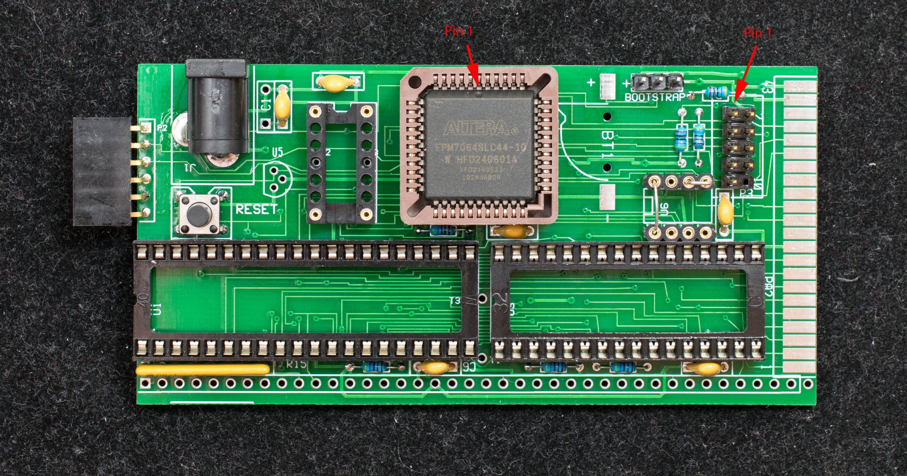
In the third picture, the PLCC socket is installed. The orientation of the socket is important, the beveled corner should be placed where the red arrow is pointed. 1x3 jumper block (T34), 2x5 programming header (P3), push button (S1), and 2.1mm x 5.5mm power jack (J1) are also installed.
![]()
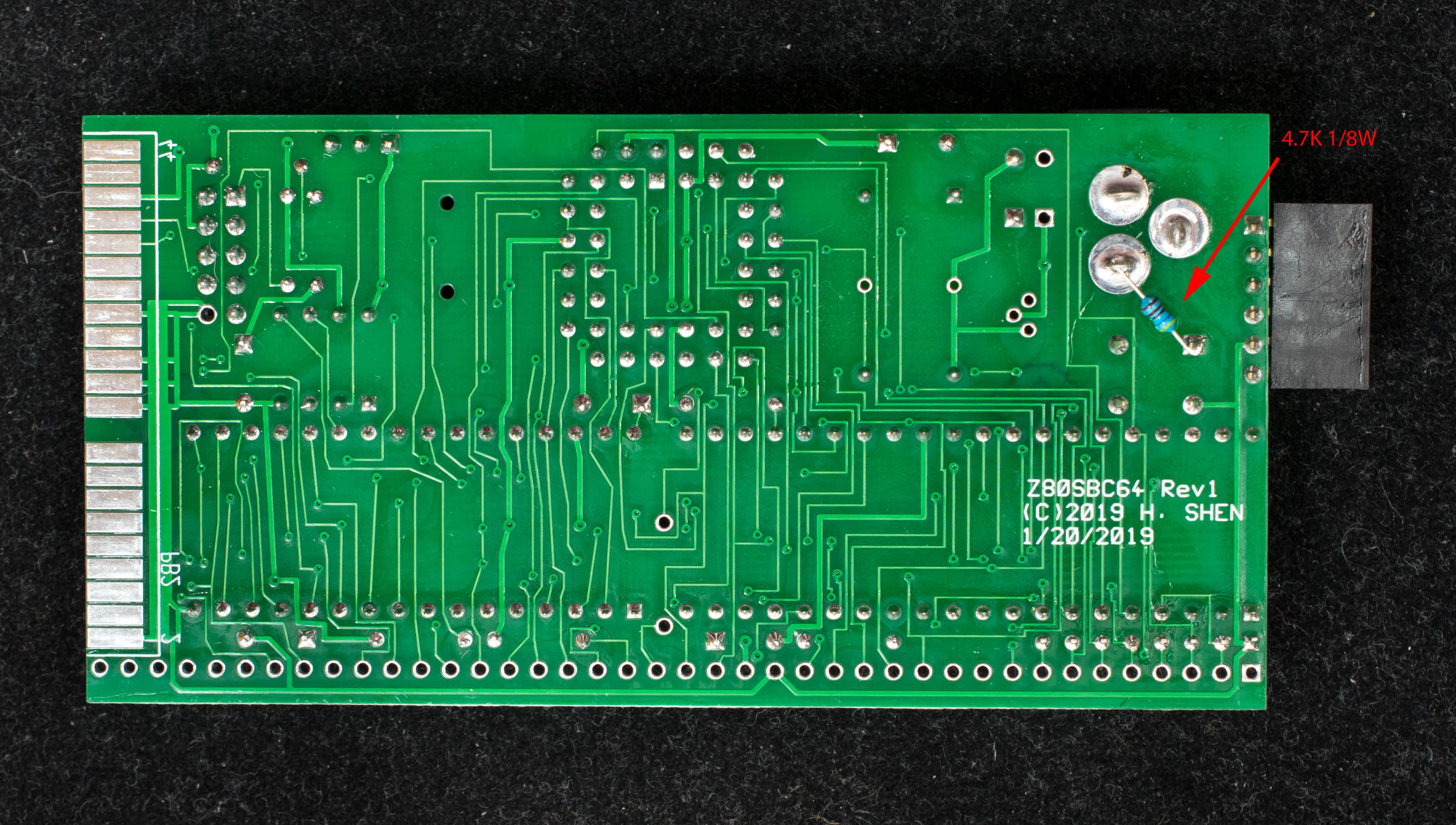
The fourth picture shows the solder side of the pc board. Because the reset supervisor, U5, is not yet installed, a 4.7K pull up resistor from nRESET to VCC is required to negate the nRESET signal. Please note, U5 may be optionally installed in this stage. If U5 is installed, then the pull-up resistor is not required.
The 1st stage assembly is now completed. The board should be cleaned with isopropyl alcohol and dried before installing components.
![]()
In the fifth picture the Altera EPM7064SLC44 is installed. Observe the orientation of the part, the beveled side with dimple in the middle must be aligned with the red arrow. Program the EPM7064 with USB Blaster, line up the pin 1 of USB Blaster cable (red strip) with the pin 1 of 2x5 header (pointed by a red arrow).![]()
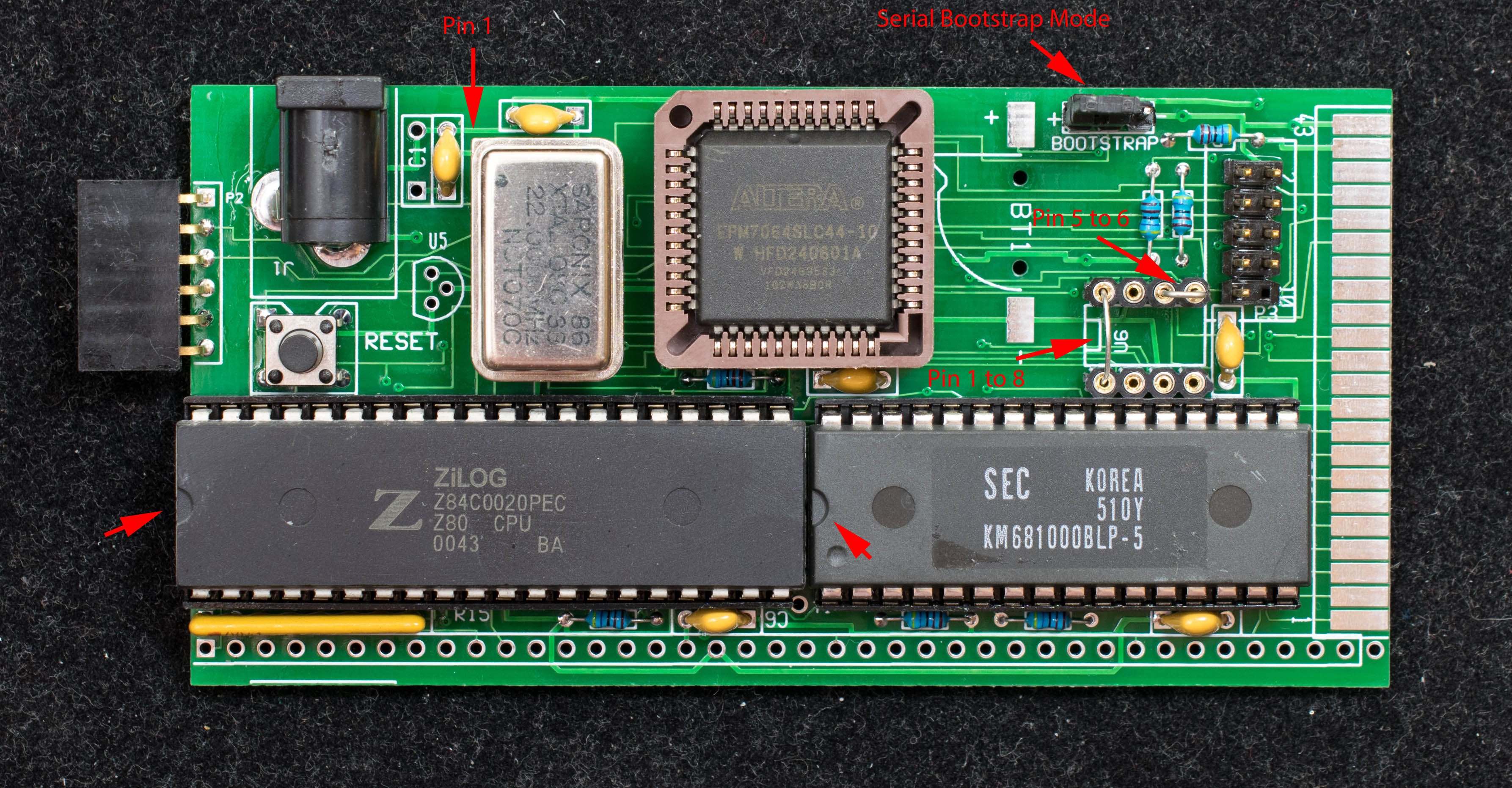
The last picture shows how the remaining integrated circuits are installed. Observe the orientation of the components. Also install the jumper to 'serial bootstrap' position as shown with a red arrow. Install two jumpers across pin1 & pin8 of U6 and across pin5 & pin6 of U6. The board is now populated and ready for power.
![]()
-
Introduction to Z80SBC64
02/09/2019 at 01:21 • 0 commentsThe z80 design is based on Z80SBC64, the '64' refers to Altera EPM7064, but as many Z80 SBC that must had been built over the years, this can easily be the 64th Z80 SBC. The current trend in low chip-count Z80 SBC is using another processor to provide bootstrap function as well as I/O functions for the Z80. Such dual-processor architecture requires complex software interaction between the two processors, and the combined throughput of the two processors are less than the throughput of any one of the processors, so it feels like stepping backward in performance and the hardware/software seems harder to comprehend and to modify. I prefer the traditional computer architecture where Z80 controls everything around it but does it faster and with fewer chips. The key is using programmable logic instead of TTL logic, but instead of the expensive FPGA that requires 5V-to-3.3V translation, using the low-cost 5V complex programmable logic device (CPLD). Furthermore, the CPLD has sufficient logic to implement an unusual feature, serial bootstrap, that uses serial port to load the traditional ROM code in RAM resulting in a ROM-less computer. The ROM-less design eliminates the hassle of ROM programming and further reduces the chip count resulting in a small 2" x 4" pc board.
The original design was prototyped with Altera EPM7128S CPLD, a 100-pin surface mount device that is difficult for most hobbyists to assemble. Further design refinements allow the final design to fit in a EPM7064S as 44-pin PLCC package. By hosting the PLCC device in a through-hole PLCC socket, the pc board can be assembled by most hobbyists. The final Z80SBC64 design is proven with successful construction and operation of 10 or more boards.
The four-stage approach is originally conceived to simplify the assembling and testing process where the partially assembled board can be functionally tested in each stage. This approach is particularly suited for hobbyists putting together a new board. It is reassuring to take baby steps and verify things are working in each step. Another issue is parts ordered may not be available or delivered, but we like to play with the partially assembled system without all the parts. Furthermore, I believe the learning process is enhanced as limitations and capabilities of the computer at each stage are explored and we learn how new features added in next stage enhances the existing capabilities.
Each of the 4 stages are breakdown into hardware phase and software phase. The hardware is the assembly phase, and the software is the testing and exploration phase. The computer is functioning at each stage and gains sophistication as the assembly progresses. It is not necessary to finish all 4 stages of assembly. The computer is functioning and may be perfectly suited for certain applications without reaching the end of stage 4.
Here are brief descriptions of the four stages:- Stage 1, minimal operating Z80, runs native monitor, SCMonitor, BASIC programs, games
- Stage 2, software are preserved between power cycles, banked memory hardware protects system software from application software.
- Stage 3, compact flash interface and CP/M
- Stage 4, RC2014 expansion bus, interface to RC2014 compatible boards
While the board is capable of 22 MHz operation, it is not necessary to run at 22Mhz. If only slower Z80, RAM and oscillator are available, it is perfectly fine to run the board at the lower clock frequency. The serial port baud rate is directly determined by the CPU clock, the table below show the relationship between clock frequency, serial baud, and RAM speed:
Clock Frequency Serial Baud RAM access time 22.1184MHz
11.0592MHz
7.3728MHz
3.6864MHz115200
57600
38400
1920055ns
120ns
slow RAM
slow RAM
Building a 22MHz Z80 Computer in 4 Stages
Step-by-step instruction on building a high-performance, CP/M-ready, expandable Z80 computer