What is depletion mode, and why you might want it
Enhancement MOSFET: normally off (the common stuff). Depletion MOSFET: normally on. To switch off an n-channel depletion MOSFET, you should apply negative voltage to gate terminal. That is, it behaves exactly the same as an enhancement n-channel, but it has negative gate threshold voltage. Very similar to a vacuum tube, by the way.
In other words, depletion MOSFET is equivalent to enhancement mosfet with built-in biasing (voltage source in series with gate terminal).
Depletion mosfets are quite rare. Chances of finding one with specs you need are much lower, and depletion mosfets are usually substantially more expensive than enhancement ones.
A JFET is a more common example of a depletion mode FET. But power JFETs are rare beasts, again.
Depletion MOSFETs are not as useful as enhancement ones, but there are a few applications where they are super handy.
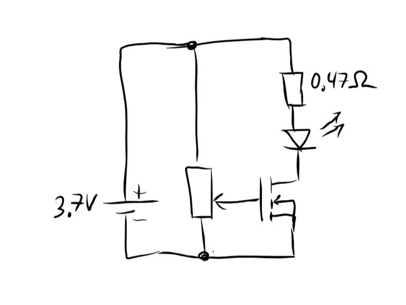
One is a voltage follower with zero or negative voltage drop. With just two components (mosfet + potentiometer), one can make a very simple knob power adjustment, that has almost zero dropout at max, and infinite input resistance. It can be used as a quick-n-dirty fan speed adjustment, LED brightness regulator, etc. See this project log for a demo of such regulator.
How to?
Modifying!
To change the MOSFET, all you need is to feed constant current into gate terminal of the MOSFET.
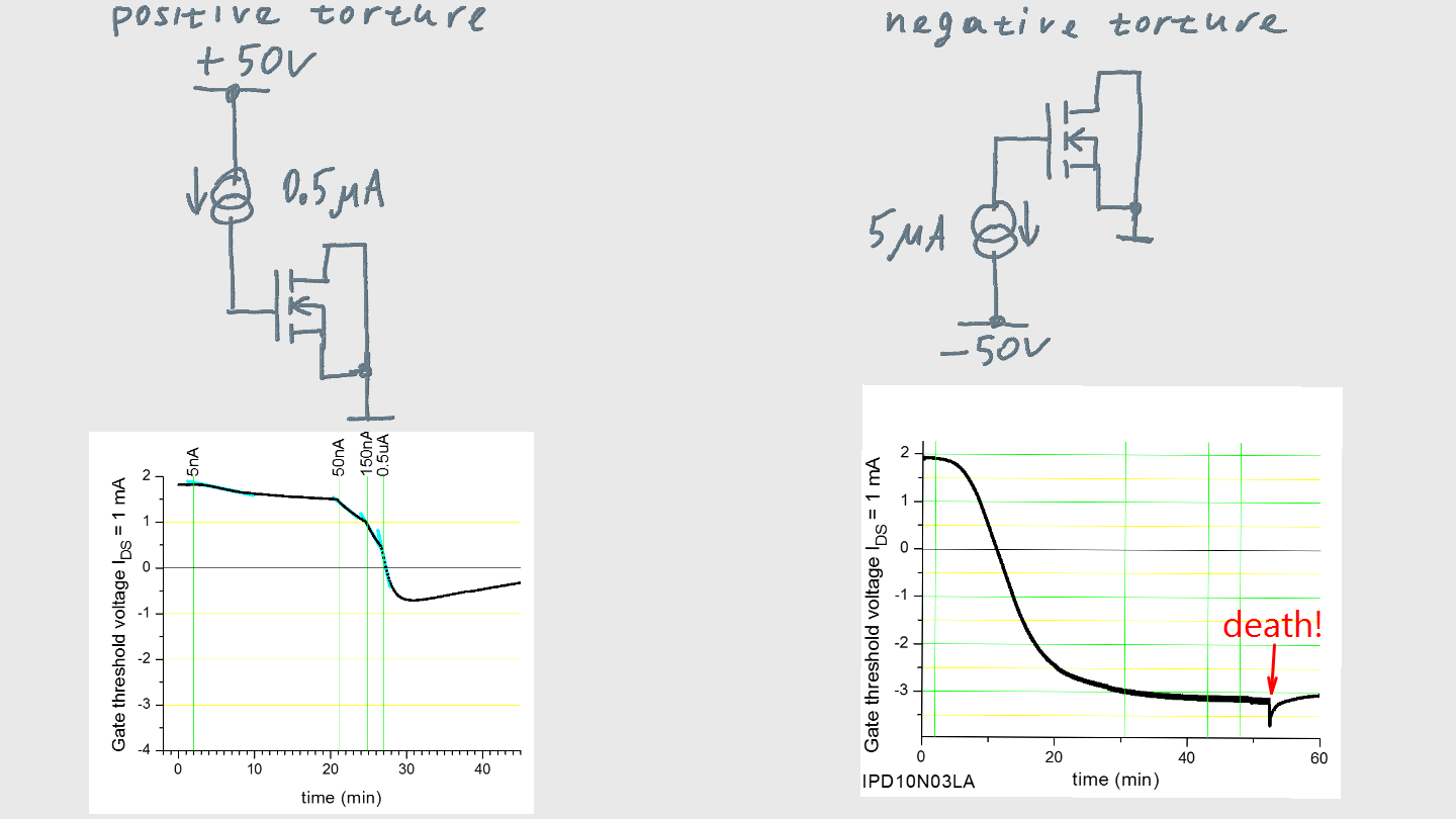
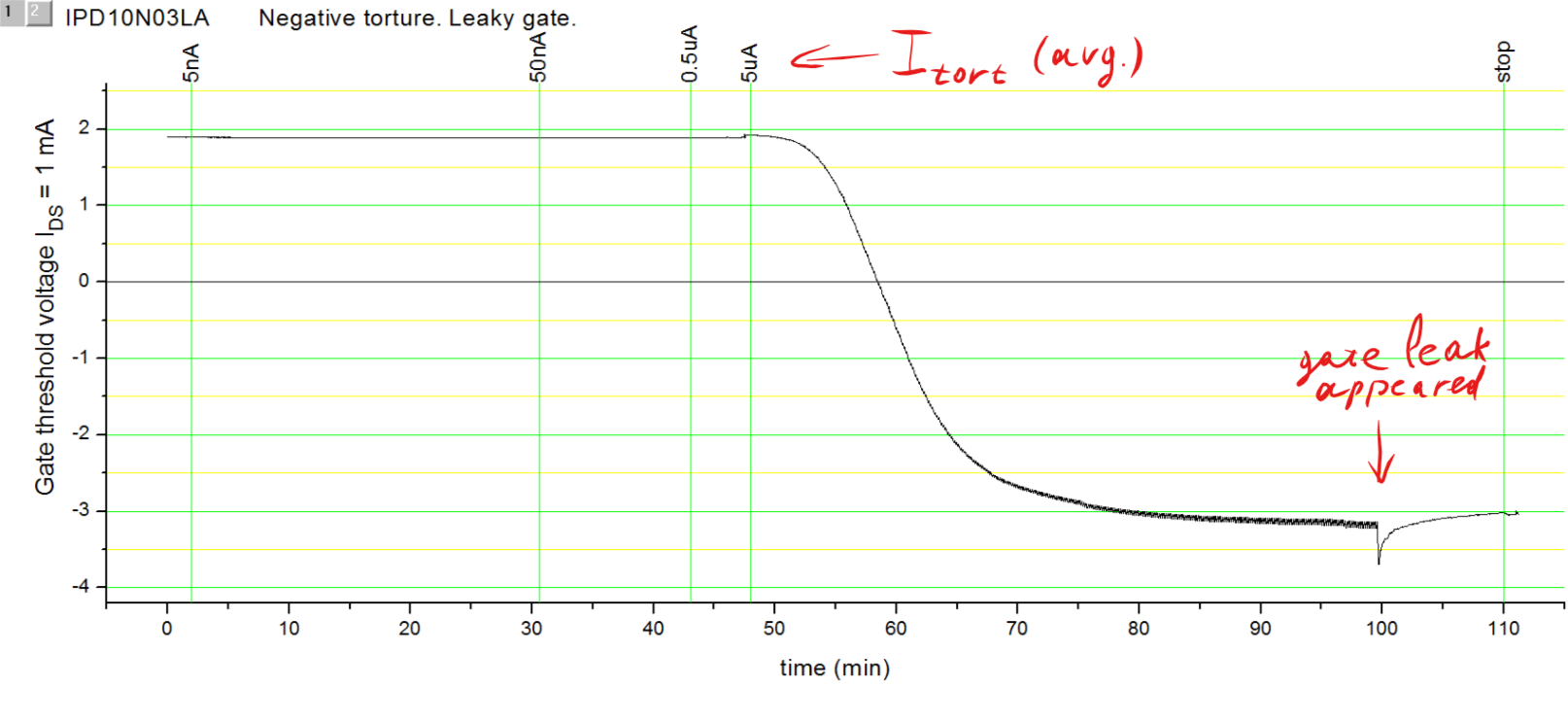
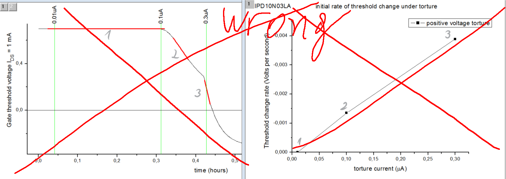
It will take around +40 V / -25 V at gate terminal or the current to start. Because it’s a deliberate violation of absolute maximum ratings of the MOSFET, I call it “torture”.
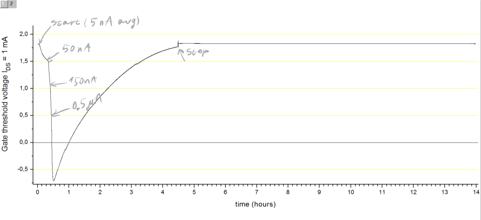
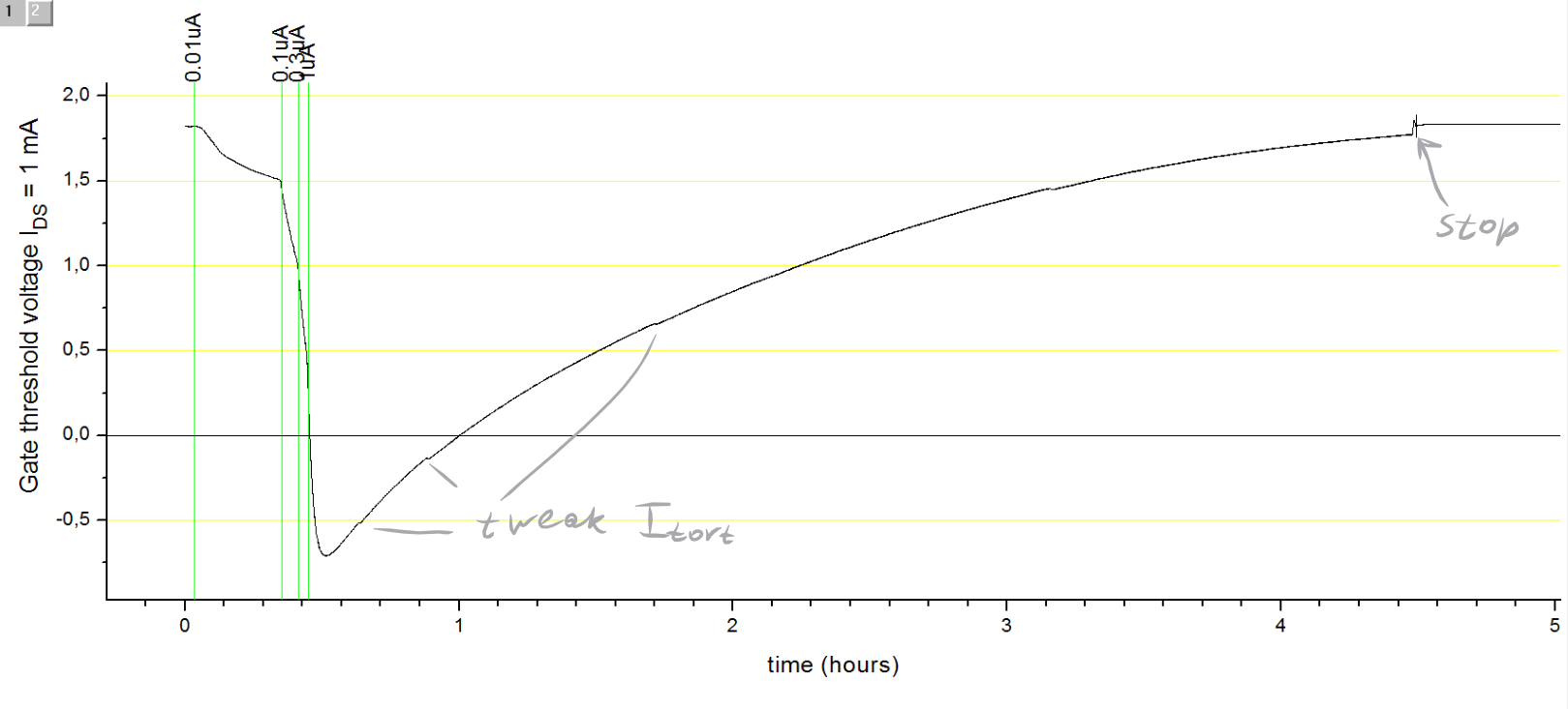
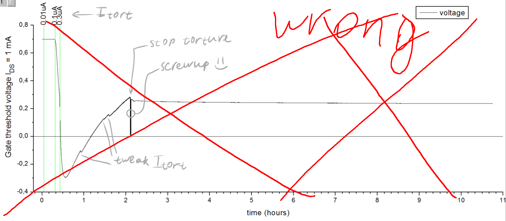
In both cases, threshold voltage goes down. Positive torture begins to change the transistor immediately, but the negative torture has a kind of lag. This lag seems to be some stray leakage that has to be overcome. The gate voltage rises to about 40 V during that lag. Also, negative torture requires more current, it can reach deeper depletion, and does not reverse direction.
So far, I was not able to make threshold voltage to increase. From that, I think that making depletion mode p-channel mosfets might be impossible (but I haven’t tried yet!).
The indicated torture currents are for Infineon IPD10N03LA mosfet, which is an n-channel enhancement mode MOSFET with on-resistance of 10.4 mΩ, 25 V max drain-source voltage, gate charge of 8.2 nC. No extensive tests on other mosfets were done so far, but I would suggest to scale torture currents in proportion to gate charge of your transistor.
@RoGeorge had successfully modified BUZ11A with positive torture, but didn’t do it in a controlled manner. See his project, #Your MOSFET is not good enough? Then modify it!.
If you successfully modify a MOSFET, let me know! (post a comment). Eventually, I hope to make a table of MOSFETS that can/can’t be modified, and torture parameters required.
Reverting!
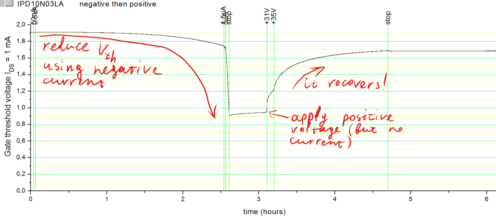
It is possible to undo the modification to a large extent, by applying positive voltage to gate. The voltage should be large, but slightly smaller than one required to cause torture leakage current. For IPD10N03LA, +35V seems to be the sweet spot.
Real-time threshold monitoring
Wondering how did I get these plots?
I made two circuits for torturing MOSFETs with real-time control of gate threshold voltage. Both circuits are chopping: the mode of operation is cyclically switched between measuring threshold and torturing.
* “blink torture” circuit – simple, but only for negative torture. Was all-right for initial proof-of-concept.
* “experimentorture” circuit – with precise threshold measurement, supporting both positive and negative torture.
Drawbacks
Sounds too good to be true? Sure, there are some problems with this conversion.
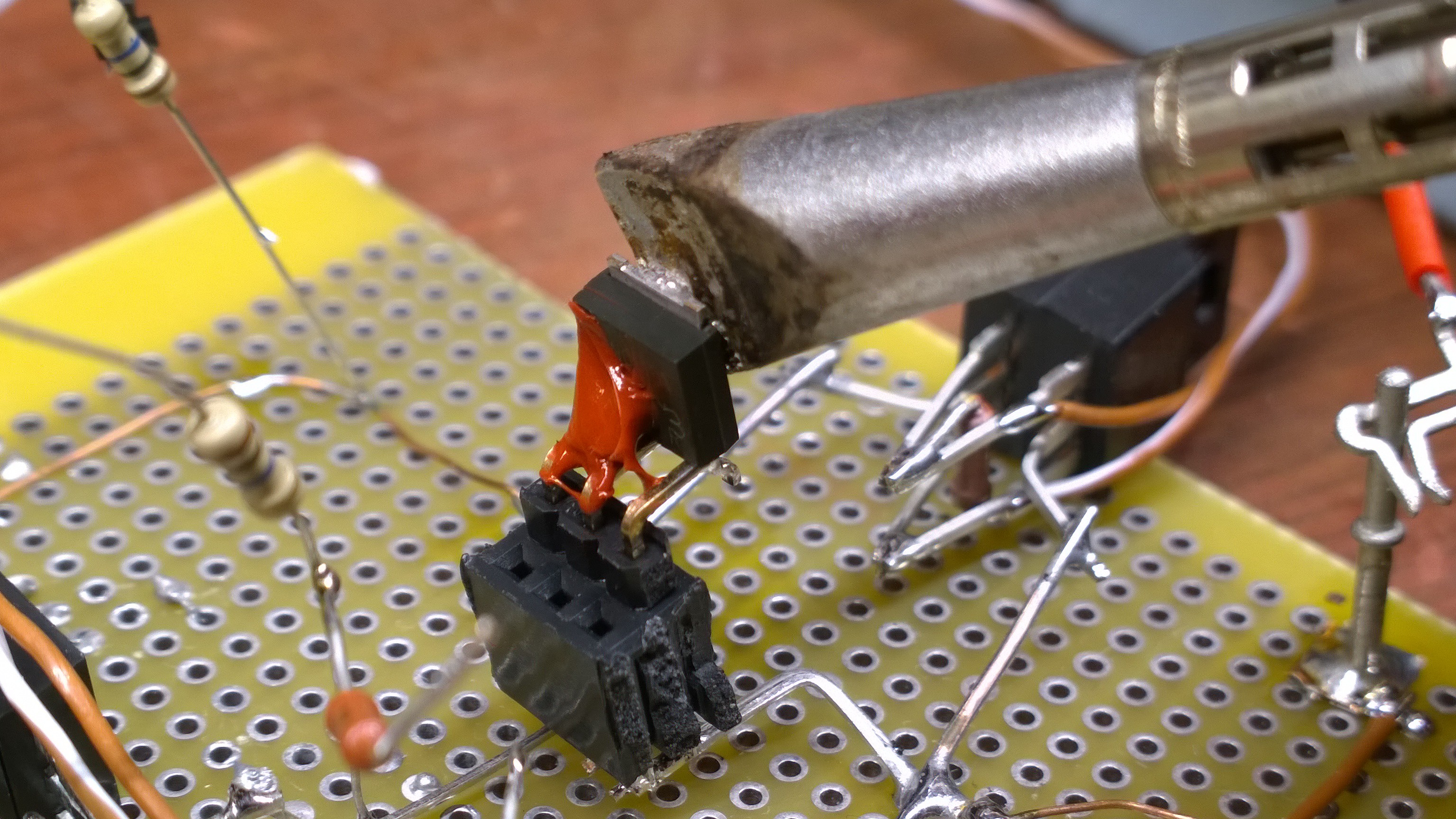
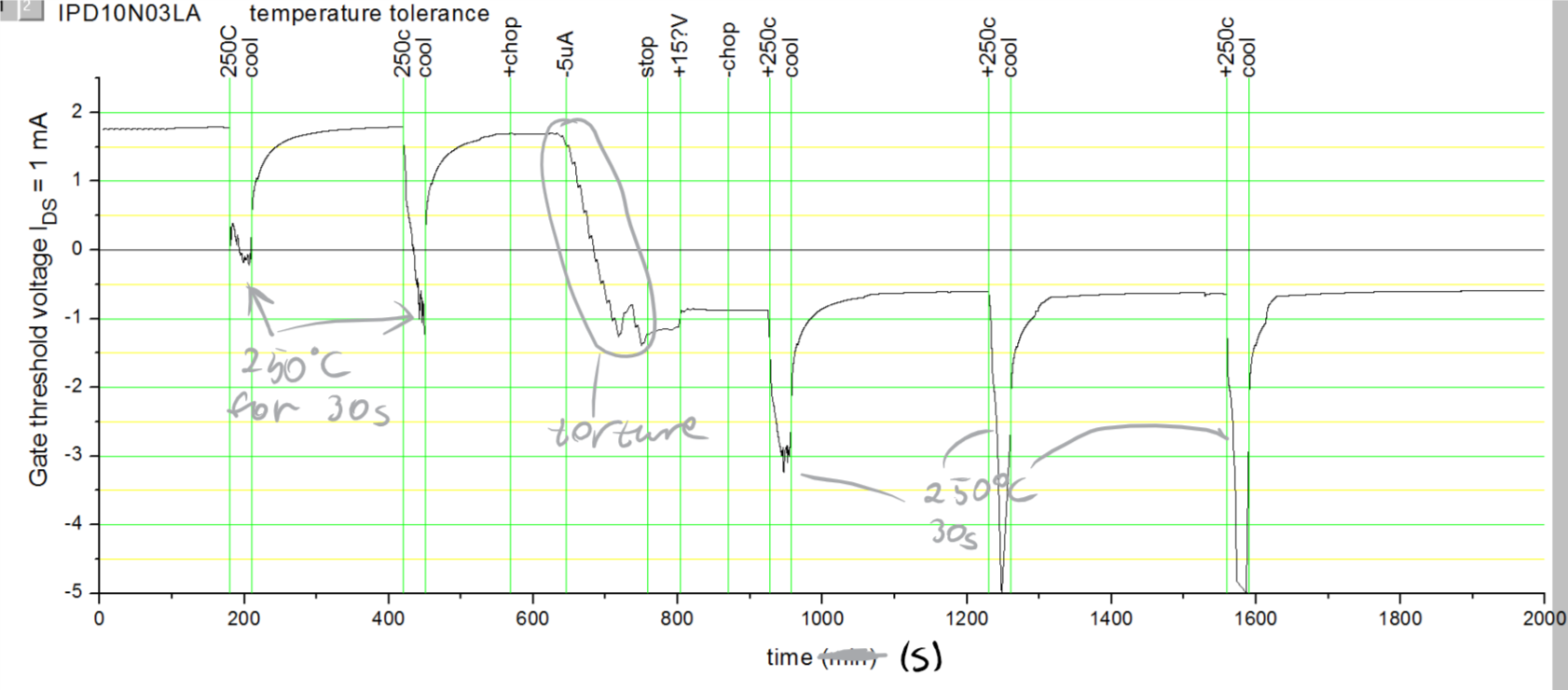
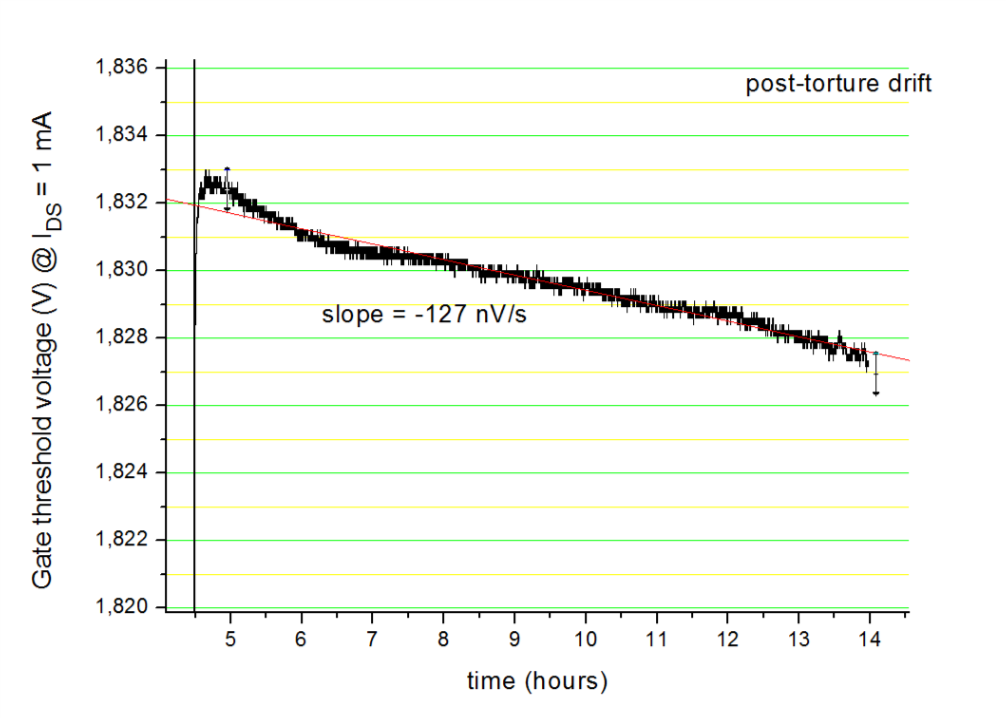
* after torture, the mosfet drifts back substantially. This drift settles out after a day or so, with substantial fraction of modification remaining. Long-term stability of the modification is unknown. However, quite surprisingly, the modification can survive soldering temperatures. ...
Read more » DeepSOIC

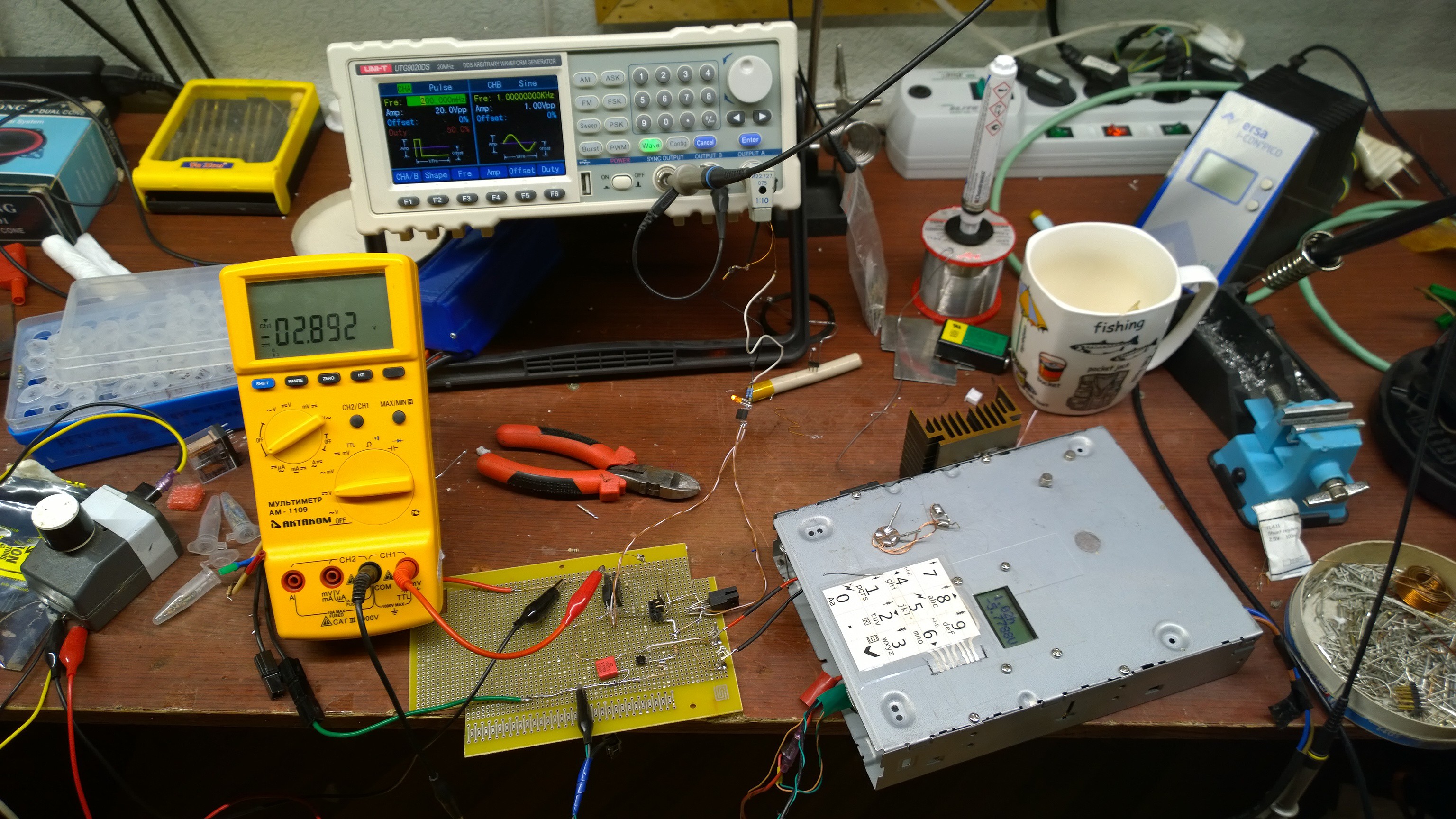
 This is the new circuit for torturing mosfets. The switches are actuated out of phase. As I explained earlier, the switches are now solid state (pairs of MOSFETs driven through photovoltaic optoisolator).




Sounds like you are trapping surface state electrons. Fets are a voltage control device and usually have a high impedance so there is limited conduction into the gate. If you hit the gate with enough voltage you can get some conduction and the electrons get trapped below the gate in the SiO2 insulator.