matseng
-
Fully analog
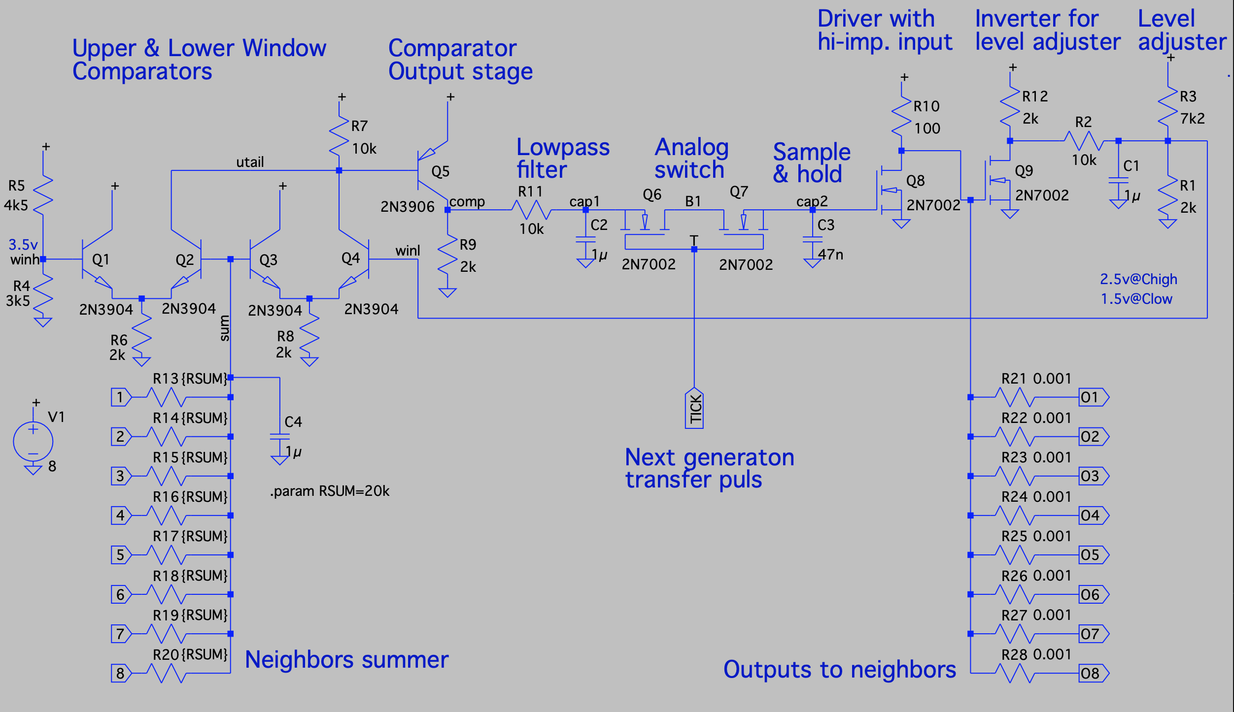
02/22/2019 at 12:26 • 1 commentI've merged parts of the other designs into a new design using only analog components and not even having a BJT-flipflop, but rather a sample-and-hold to keep the state from just racing around the entire design uncontrollably.
![]()
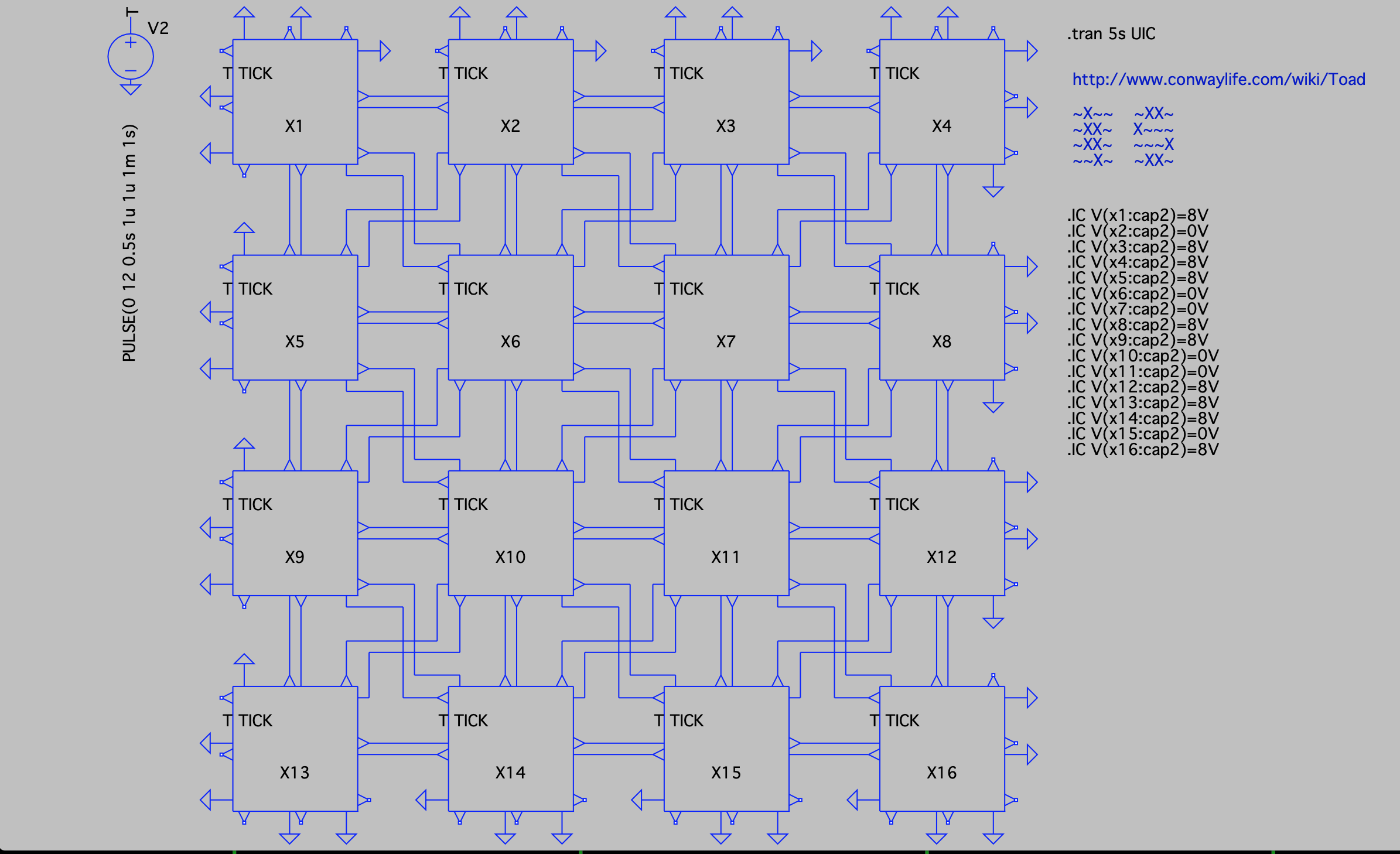
Running a simulation with a 4x4 matrix of these and adding the "Toad" pattern as the initial charges on the C3 sample&hold capacitor it runs just fine.
![]()
I'll probably make a pcbs for this and add a few dozen of them to my next pcb order and see if they run in real life as well.
-
Low part count version
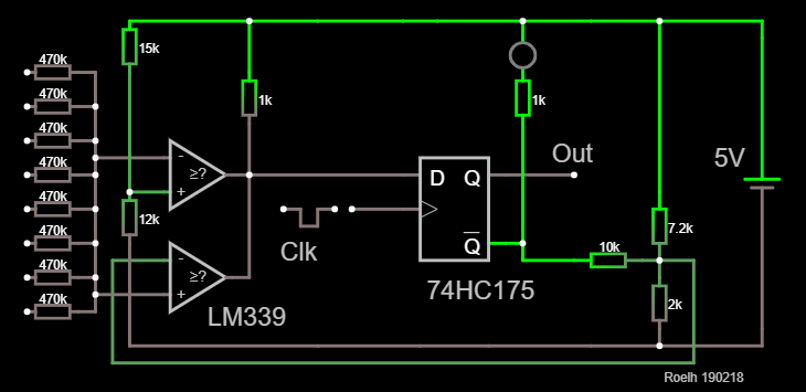
02/18/2019 at 18:18 • 2 commentsI don't know if the rules forbid the use of a flipflop.... But the state of a cell is digital, isn't it ? So we use digital building blocks for that part.
![]()
So a part of the previous design was replaced by a flipflop.
From a practical point of view, it seems logical to place several cells on a single pcb, for instance 16.
Each cell needs 1/2 LM339 and 1/4 HC175, so for 16 cells this is 12 IC's.
The reset input (not in the diagram) of the HC175 can be used to reset the system to all zero. There should also be a possibility to pre-load a certain pattern, or several patterns (to be determined).
-
Proposal based on quad comparator
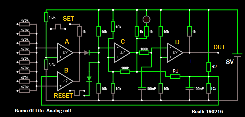
02/17/2019 at 09:46 • 18 commentsThe following circuit shows a possible way to do this. It uses a quad comparator similar to the LM339. Note that these can only sink current at their output, so they need a pull-up resistor. It also means that the outputs can be connected together to form a wired AND gate.
![]()
I use an 8 volt power supply, in that case the voltage at the summing point will be (almost) equal to the number of surrounding active cells. Easy for measurements. But it will work with other voltages too. I here assume that the comparator outputs are almost equal to GND or VCC.
The opamps A and B form a classic window comparator. The upper one compares to 3.5 V, the lower one compares to a voltage determined by R1, R2, R3. These resistors should be calculated such that:
When the output of C is HIGH (cell dead), the voltage of the - terminal of B should be 2.5V, and
When the output of C is LOW (cell alive), the voltage of the - terminal of B should be 1.5V,
Comparator C holds the actual state of the cell. In each cycle, it gets a short negative-going reset pulse followed (or partially overlapped) by a positive going set pulse. The set pulse will only be effective if the set-signal is not shorted to ground by the window comparator. The C comparator has positive feedback so the state is remembered. The output drives a LED if the output is LOW, that indicates if the cell is alive.
The output of C is connected to the inverted input of D, that delivers a active-high signal for the neighbors. Note that there is a low-pass filter that keeps the output from changing while the pulses are applied. The output of the R1,R2,R3 circuit also has a capacitor with the same purpose.
No tests or simulations were done yet, so it might be needed to do changes. It might also be possible to simplify the circuit. Note that the input summing resistors could be in a single resistor array. It should be checked that the comparators have sufficient input range.
-
555 bending
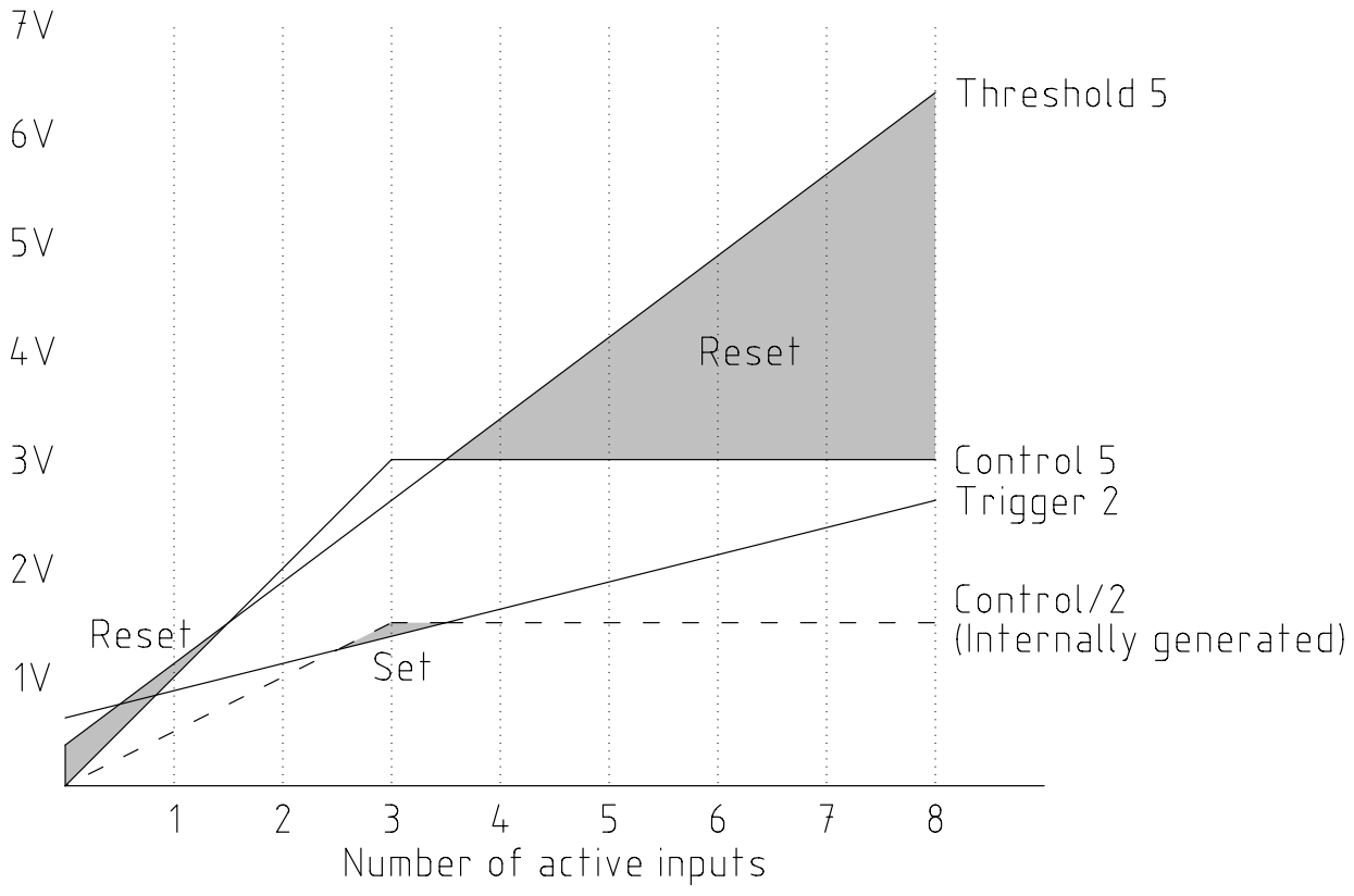
02/16/2019 at 04:22 • 6 commentsSo it turns out Conway's Game of Life is more complicated than I thought. I was under the impression it turns on a cell when there are sufficient neighbors, and turns it off when their are too few neighbors, which is exactly what a 555 timer does on an analog level. Easy peasy.
But apparently it's more complicated than that, in which it turns off a cell if there are too many or too few neighbors, and turns it on if there is an exact amount of neighbors. Which is not what a 555 timer does. Not easily anyway.
I had claimed this can be done with a single 555 timer, and I won't let a simple misunderstanding of the concept the entire project is based on slow me down. The 555 alone isn't really enough, so I threw in a zener diode to give me some nonlinearity to play with. (I have a few oddball computing projects in the works and have found out just how useful a tiny bit of nonlinearity can be). I made a sort of analog truth table:
![]()
The biggest issue I see with this is that some comparisons are only made by 125mV. This should be enough, and can be dialed in by adjusting power supply voltage relative to the zener diode, but it's still a concern. I'll have to prototype something to know for sure whether it can work or not.
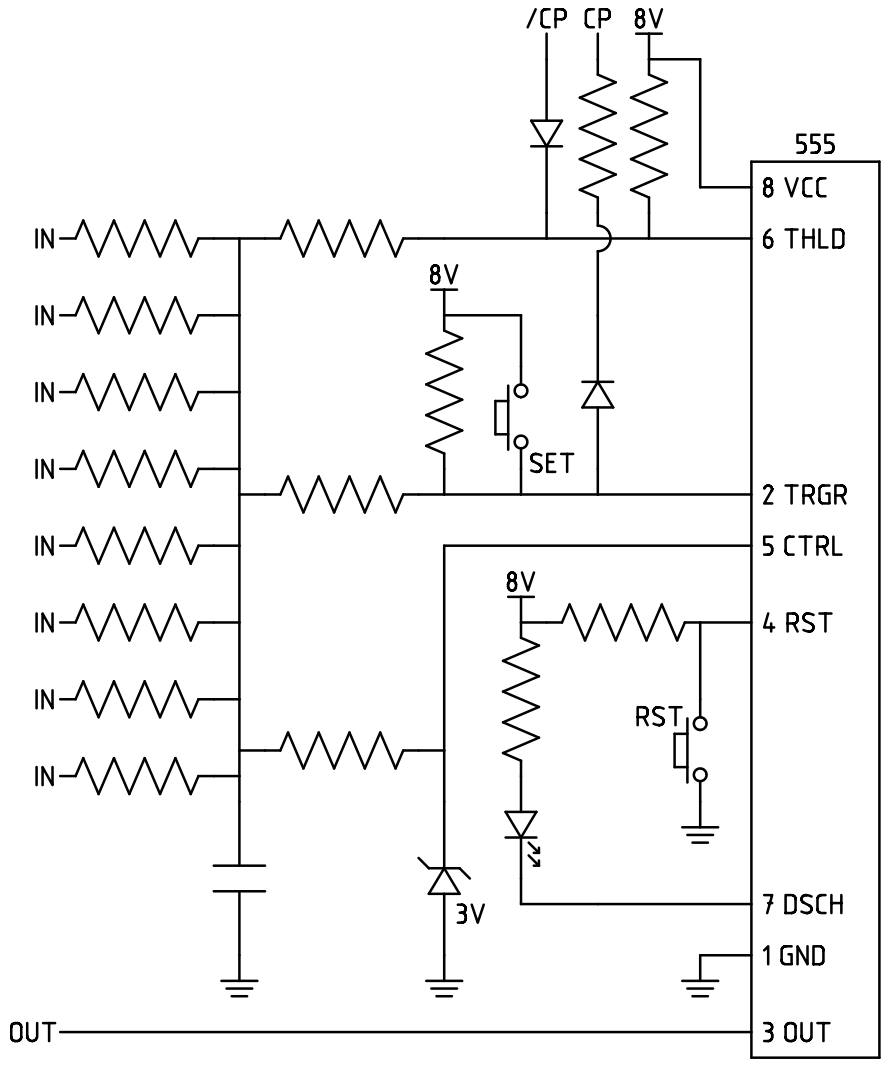
Here is a schematic that should achieve something close to that:
![]()
Clocking is handled by holding the comparator inputs too far away from it's other input to ever trigger the flip flop. Setting works by forcing a comparator to trigger the flip flop.
Another obvious problem, is that resistors have to get progressively larger in value for later stages to not affect earlier stages. I'll have to see what the CMOS version of the 555 timer requires. It shouldn't take too much current, so something on the order of 47k for the later stage resistors should be fine.
I haven't yet done the math as to what the resistors should be, but it is simple to do from the first diagram.
This is of course just a design suggestion and not a final schematic, so input is welcome.
-
PCB interconnects
02/14/2019 at 17:11 • 0 commentsSince I want to make it fully modular I need to have each PCB (pixel) both send its state to all eight neighbors as well as receive the neighbors states.
I gave this problem statement, together with a strict rule of "don't cross the streams (wires)", to my wife and she came up with something looking like this:
Initial interconnect plan Not bad at all actually. But after looking at it for a while I realized it could be improved slightly by removing a redundant connection in the pass-troughs.

Improved interconnect scheme This could also be slightly improved by switching the horizontal interconnects to reduce the trace length on the PCB a bit.
I also need to add PWR and GND between all PCBs, but there's enough space for that at the left/right edge.
anaGoL - Conway's Game of Life the analog way
A design for a non-microcontroller / non-digital logic Conway's Game of Life cellular automata simulator