So I talked in the previous log about how I had some issues while integrating the MC68901 MFP that I initially assumed were hardware-related, but that turned out to be software. Once I got past that, I hoped it would be plain sailing. Boy, was I wrong.
---------- more ----------
This morning, I took delivery of a 1.8432MHz crystal, which is perfect for generating the standard Baud rates we're all used to. I was quite excited to hook this up and then write a bit of code to just send something, anything, via the UART and a cp2102 UART-to-USB board I had lying around.
I hooked up the crystal, and quickly put together a bit of code to set up the timers and enable the transmit side of the UART. Needless to say, it didn't work first time. No problem, I didn't really expect it to. I still had the BIN files of the previous ROMs kicking around so I burned them back to the chips so I could watch the lights blink while I fixed the code. It was at this point that hilarity ensued.
The board was dead. The ROMs can't have burned correctly, so I burned them again. Still nothing.
I assumed that the jury-rigged EEPROM burner I built from a NodeMCU and some flip-flops must have stopped working. I don't have another one, so I built a quick circuit that would let me manually flip the address lines and see the output on LEDs. The first and last few bytes in the ROM matched with the bytes in the BIN I'd burned.
At this point, I ordered a real EEPROM burner, just to be on the safe side. Also because I was tired of using my home-built one which still required me to recompile the NodeMCU firmware to change the data that got burned to the ROM.
I spent a few hours checking and rechecking all the connections around the ROMs in case I've dislodged something while pulling them for programming.
I'm now thinking I've killed the ROMs with ESD or something when I pulled them from the board to burn them. I order more ROMs, just to be on the safe side.
Again I'm deep down a rabbit hole with only a multimeter and cheap logic analyzer for company. The readings I'm getting are all kinds of weird (at one point I'm assuming the 68010 is broken, because I'm not seeing the first word read of the initial SSP - turns out the logic analyzer just needed to be unplugged and plugged back in again).
Finally, just as I'm about to give up until the new ROMs arrive, I decide to try one last ditch thing (which really ought to have been my first-ditch thing, but oh well) and delete all the old BIN files and build them from source.
Bingo. All working fine again.
The "previous ROM" BIN file turns out to actually be an incorrectly-named version of a much earlier memory test program I wrote, which spools through the entire address space. This includes the expansion space, which now doesn't have any DTACK generation (since the changes I made to support the MFP) and helpfully no longer has a working indicator LED (because I've kind-of abandoned the idea of expansion space in the current revision due to the output line from the decoder being not-really fit for purpose, more on that in another log).
So all the while I thought the board was dead, it was really waiting patiently for a DTACK that would never come, in an address-range that I don't have an indicator for. I did think it was weird that the run LED never went out, but just didn't connect the dots.
It's been a very frustrating couple of days on the m68k project. All my own fault, of course.
Some background: I've been hooking up the MC68901 MFP which will give me some GPIO capabilities, a UART (actually a USART but I'm not using the S), some timers and support for vectored interrupts. All was going pretty well - it's a lot less wiring than most of the other chips on the board (five address lines, eight data, a few control lines and a bit of extra glue logic).
---------- more ----------
Because I want to use it for vectored interrupts, its eight data lines have to be wired to the lower half of the MC68000's data bus. The 68901's data strobe is then hooked up to /LDS on the CPU, allowing the chip to supply the needed data at autovectoring time. This set-up means that the MFP's registers are all accessed at odd addresses - in my case, it's mapped into IO space so the registers start at 0xF80001 and occupy all the odd addresses up to 0xF8002F. For the code, I decided to put these into a separate file I could include in the main assembler source (extract below).
With all the wiring done I added a bit of code to the existing ram test program (on Github) to initialise the MFPs GPIO and toggle one of the lines after each run through the RAM, allowing me to hook up an LED and get some visual feedback that the MFP was working.
In short, it didn't work. Worse, it made the whole board hang. Time to start debugging then!
I quickly realised (thanks to my address decoder blinkenlights) that it was hung waiting for DTACK, for an address in IO space. I've built a simple circuit that takes care of that specific situation (as the MFP likes to generate DTACK itself) so immediately assumed that wasn't working. I don't (yet) have a watchdog on DTACK to generate a bus error, so if DTACK isn't acknowledged, currently the CPU will just wait forever.
I broke out the meter and the analyzer and got to work to find out why the IO DTACK generator wasn't working. I discovered it was working fine.
I checked the 68901 was receiving the requisite 4MHz clock from the divider I put on the system clock. It was.
I checked the voltages around the board, and noticed they were still a bit shaky. In light of this I switched from the old daisy-chained power setup that has grown with the board to a star setup and threw some more capacitors on. The voltages were now rock solid (still a bit more drop than I'd have liked but well within tolerances) and the board still didn't work.
I checked all the connections, and found I'd accidentally wired the output of timer D to one of the address lines instead of the transmitter clock line. Since I wasn't enabling the timers yet I figured this wasn't the problem, but fixed it anyway. It wasn't the problem.
Eventually I realised that the CPU wasn't asserting LDS as expected for an odd address, and was instead asserting UDS. Cue several WTFs, more continuity checks to make sure I hadn't wired UDS and LDS backwards into the bus (I hadn't), and a serious amount of head scratching.
After a (long) while spent re-reading the CPU datasheets, staring at the code, checking various connections and swearing, my mistake dawned on me. You see, the extract of code above is the fixed version. The original had lines like this:
MFP_GPDR equ MFPBASE + $01
Which, with the assembler I'm using (I'm still using Easy68k for quick stuff as it has a convenient way to dump odd/even binaries) means "Set MFP_GPDR to 0xF80000, and then ignore the rest of the line because it's a comment". 0xF80000 is an even address, and all the registers were mapped there. The CPU is asserting UDS correctly instead of LDS. Lack of LDS means the MFP isn't aware it's supposed to be generating DTACK, and so it doesn't.
Cue major facepalm. Removing the spaces fixed it right up, the code ran perfectly, and the LED on the GPIO line flashed away merrily. I'd also fixed the power issues (which I've been putting off for a while) and tidied things up a bit, so I considered it a win (admittedly, a hard-won one).
You'd think after struggling with that for the best part of a day, getting the UART working so I can finally see something on a screen would be a piece of cake, right? Well, you'd be wrong. Stay tuned for part two...
Now that the board is reliably running code (more on that below) I'm into the next stage of planning, which will involve hooking up the MC68901 MFP (Multi-function Peripheral). This will give me some interrupt timers (meaning I'll have a tick for the kernel to use) and a USART which I'm going to use for the initial IO to an external terminal (via a USB converter).
Most of the work here will be simply connecting it to the bus, but it will mean DTACK-grounded isn't going to cut it any more, at least when /IOSEL is asserted. With that in mind, I designed a small circuit that will look after DTACK for me:
---------- more ----------
This is super-simple, and is effectively the same as having DTACK grounded when RAM or ROM is selected (ignoring a bit of propagation delay of course). When IO is selected, however, it allows DTACK to be controlled by an external active-low signal, just like the one the MC68901 provides.
Gating the whole thing with AS is probably not necessary (and may even be undesirable - I won't really know until I build the thing and look at it with the analyzer) but felt cleaner.
Of course this is still the minimum-viable solution, but it will work for now. As the system grows DTACK generation may well become an issue again, and if it gets much more complicated I have a vague plan to move to an arrangement where DTACK can be generated by any one of a number of open-collectors which I'll wire-OR together.
A (hopefully) final update on reliability
Following my last couple of logs, I thought I'd nailed reliability. However, I noticed that it would still go wrong very occasionally. Everything would run fine for anything up to an hour or two, and then it would go wrong and end up asserting HALT.
This was really annoying, and I was thinking of all kinds of strange and exotic things - interference, weird timing-related things, a faulty chip? Then, while looking at something else with the multimeter I noticed that the voltages on the board were all over the place. The daisy-chained power connections between the breadboards were the problem, and putting in a couple of jumpers directly between the two ends of the whole system cured it (longer-term I plan to redo the power connections so there's no daisy-chaining).
Just goes to show that in homebrew computers, as in almost everything else, debugging should start from the basics. I'm happy to report that the board has been running now for a solid 24 hours without a glitch.
As I mentioned in yesteday's log, I finally got the computer to run some code from ROM, but that is was unreliable and always seemed to wander off into oblivion after some time (a few tens-of-thousands of microseconds).
---------- more ----------
From doing a lot of poking and prodding, and running trace after trace with the analyzer, I thought this was related to timing. My ROMs should be fast enough (just) to run with DTACK grounded, but clearly something was off.
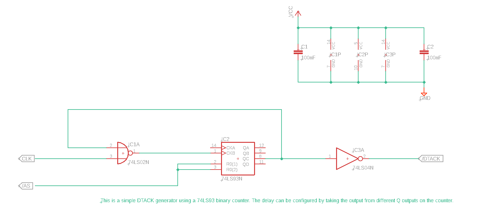
For testing, I jury-rigged a DTACK generator using a 74LS93 binary counter in 3-bit mode. It looks like this:
And here's a trace showing how it looks compared to AS (40n between dots): (Good thing I read Matt Lacey's awesome log about DTACK before I designed this, or I'd probably have come up against the same problem he did first time around!)
This seemed to improve things, but the problem still remained. I figured I'd sleep on it.
Fast-forward to this morning, and while trying out some changes on the board I realised that having my hands near the CPU kind-of fixed the problem. Uh-oh, something's floating.
Some sanity checking and continuity testing later led me to discover that, because of a mistake in the control bus wiring, my new DTACK generator was in fact trying to drive the CPU's bus-grant line. DTACK was in fact floating, and it was purely random chance that it ran at all.
Having fixed that, I first verified that the DTACK generator works (it does), and then went back to DTACK grounded. It now works perfectly and has been happily sitting my bench for the last hour, running this code which gives me some visual output on the address decoder status LEDs.
I've also made a small change in the ROM wiring to ensure it's safe to have DTACK grounded. Where I was previously using the address decoder to drive the /CS lines, I've instead tied CS low and am driving the /OE line from the decoder. According to the Atmel ROM datasheet, that should about halve the time-to-output from 150ns to 70.
After a frustrating few days, the rosco_m68k is now successfully running code from the EEPROMs! It turns out I'd wired the ROMs to the wrong half of the data bus (facepalm, endianness again), and also needed to make a few other tweaks to get it working.
---------- more ----------
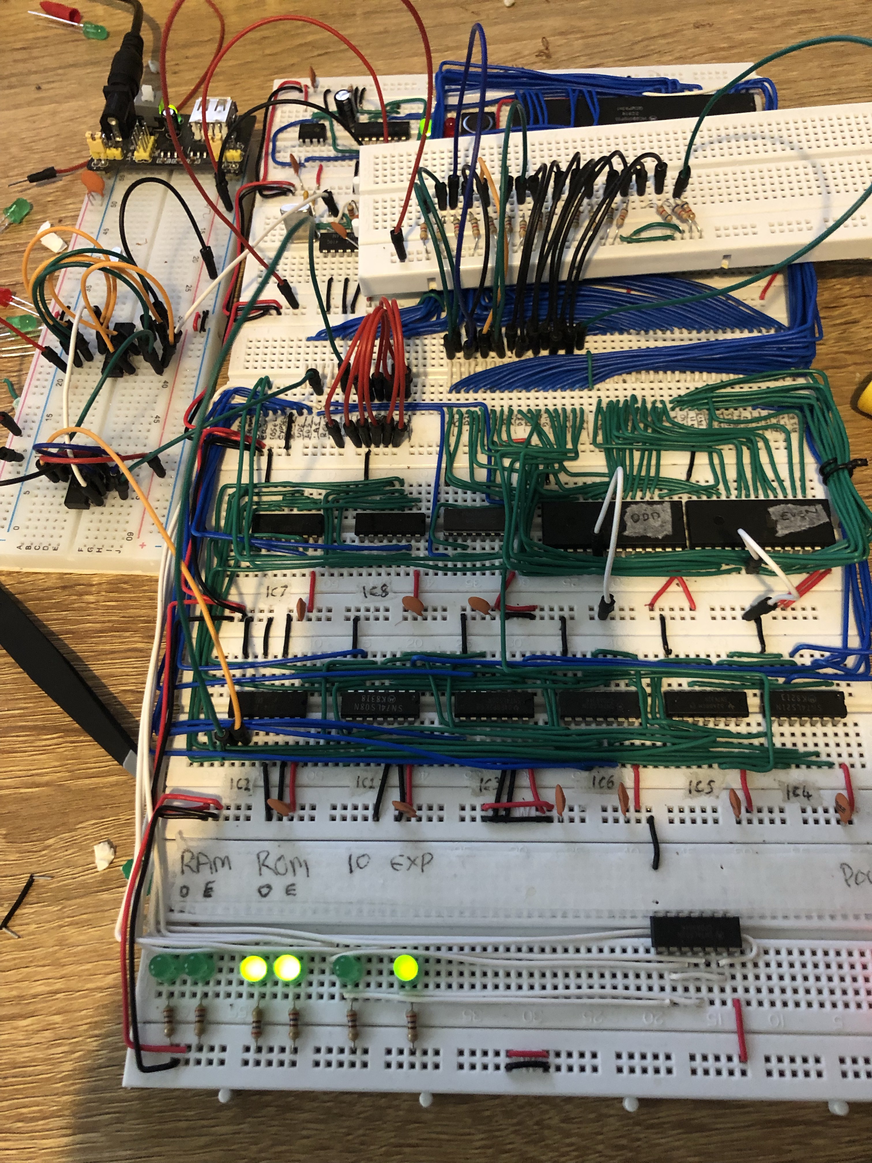
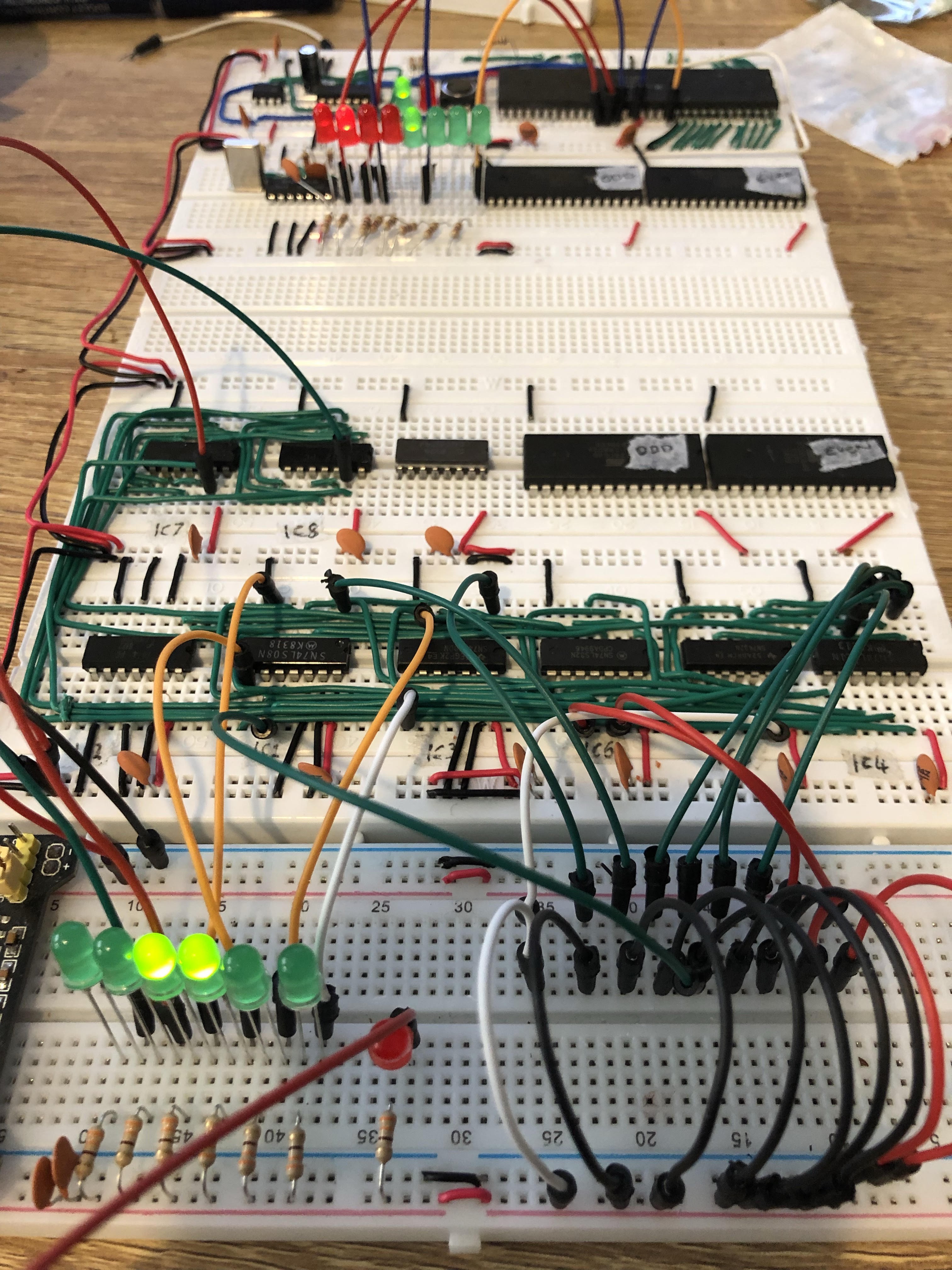
The board currently looks like this (with a few not-yet-permanent fixes):
The key differences are:
DTACK is no longer grounded. The upper left breadboard in the picture contains a (temporary, but possibly soon to be permanently wired on the main board) DTACK generator based on a 74LS93 binary counter (in 3-bit mode) and a NOR gate. This is driven by the AS line (which drives the counters reset line) and the CLK, with DTACK being generated by the negated output of Q1, Q2 or Q3 depending on how long the delay needs to be (hardwired configuration right now).
Theres also an extra breadboard plonked on top of the main board in this pic, which is just a bank of resistors that are weakly pulling the data bus high.
Both of these changes are attempting to improve reliability. While the system does properly boot every time and starts running code, it occasionally wandered off into the wilderness and ended up double faulting (and asserting the HALT line).
The DTACK generation seems to have helped quite a bit in this regard - without it, the system felt a lot less reliable that it does with it. Sadly though it's still not 100% - although it will often run for several minutes it usually ends up halting for some reason.
But for now, I'm just happy it's doing anything at all - I've been a few days figuring out what was going wrong, and with only 8 channels on my logic analyzer it's been a challenge to try and see what the various bus lines were doing.
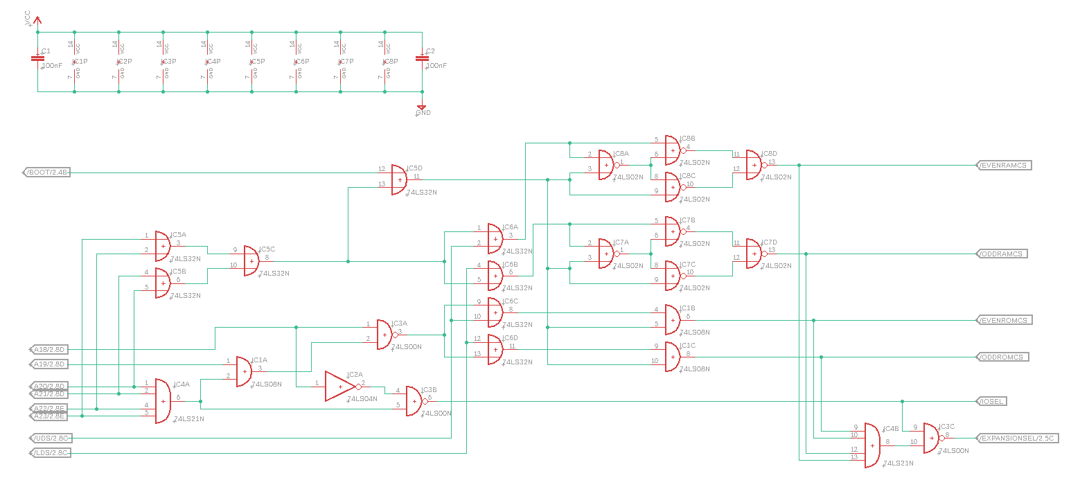
While building the address decoder, I realised I'd made a couple of mistakes in the design. Now they're fixed, I'm posting the updated schematics (They're available on Github as usual, too).
---------- more ----------
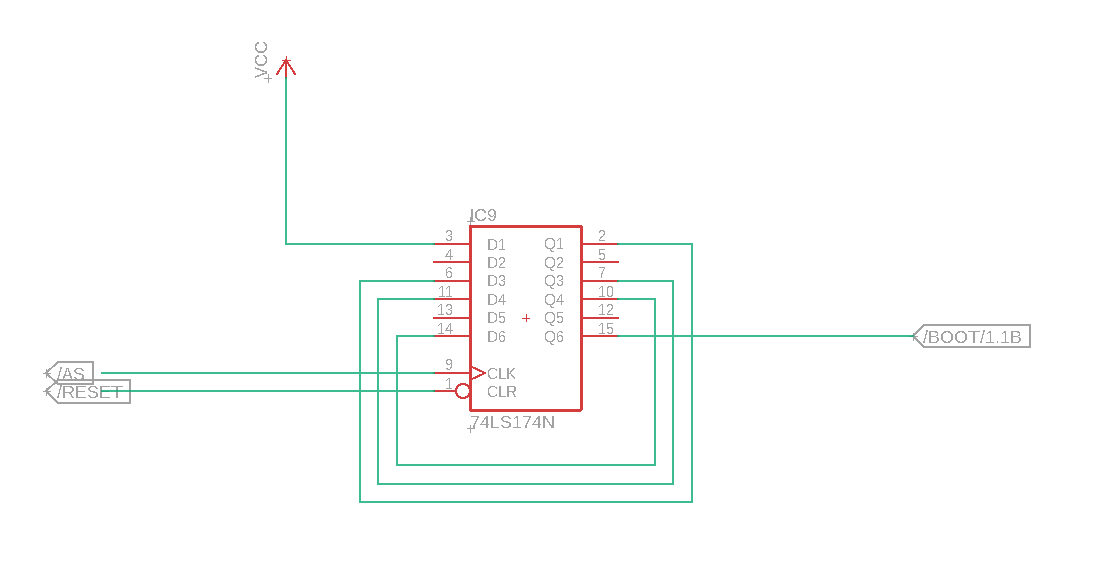
Here's the updated address decoder (The main issue was that the /UDS and /LDS lines were handled backwards in the v1 schematic): And here's the circuit that handles the /BOOT line:
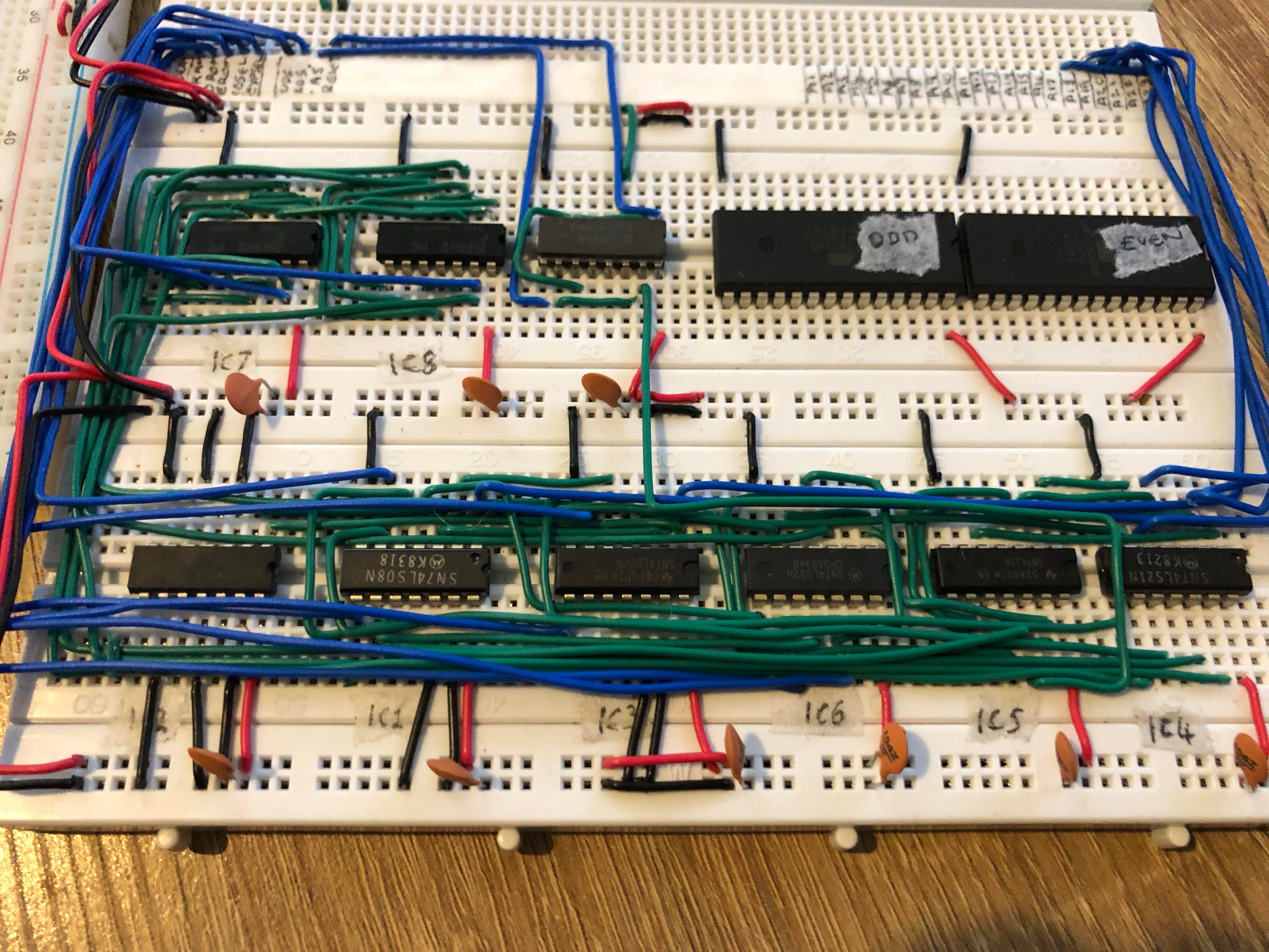
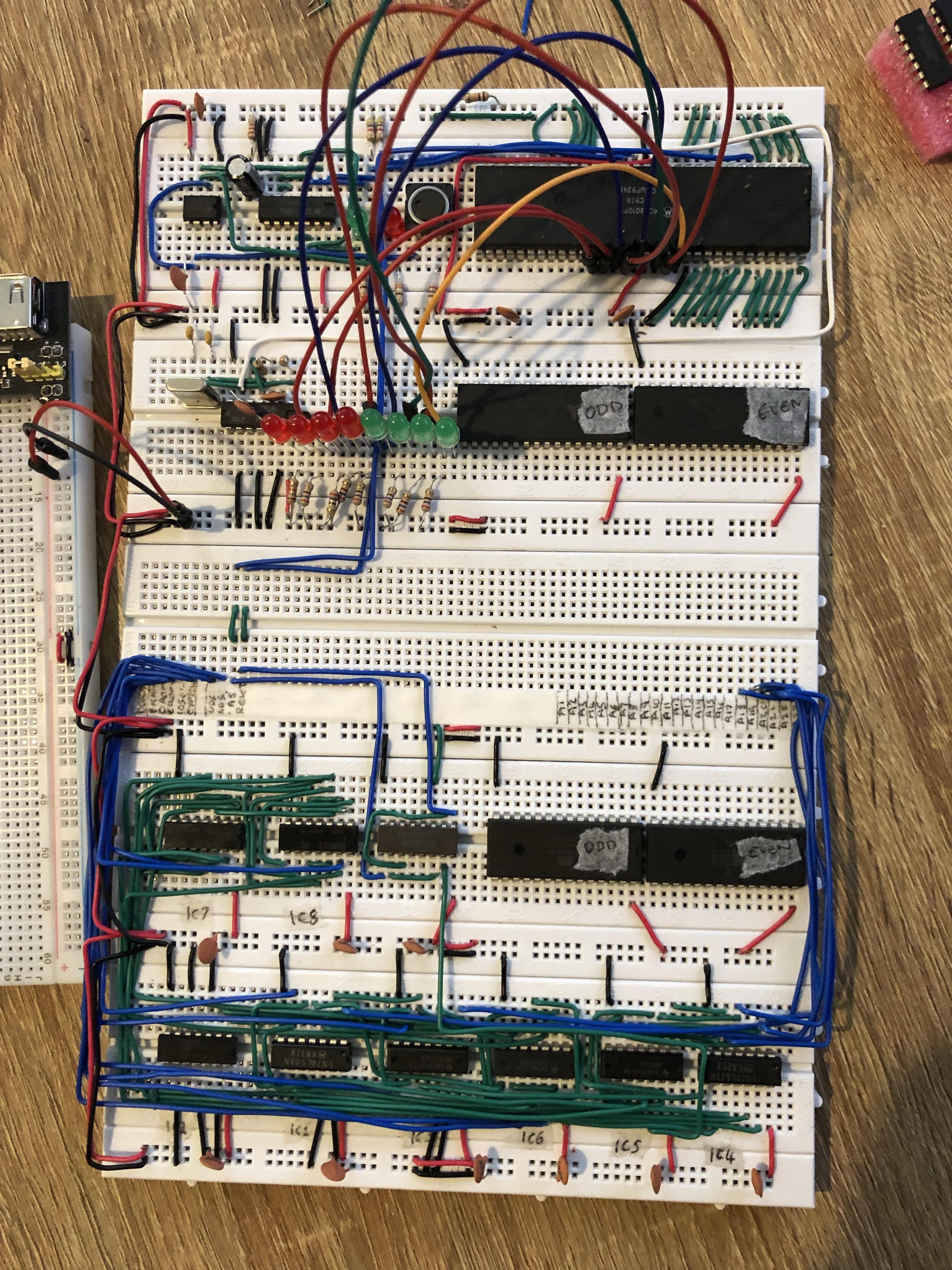
So I finally gathered all the parts I needed, and since I have some time off work this week I managed to build the address decoder. I'm happy to say it was fairly painless although time-consuming - routing all the wires has taken the best part of a day. To be fair, a couple of hours of that were spent debugging a couple of mis-wired connections though.
It looks like this:
---------- more ----------
This handles all the address decoding I've talked about previously, and has the /BOOT line generator as well (the slightly out-of-place looking IC in the center top is a DM54174 - a military-grade variant of the 74174 Hex-D Flip-flop I found in my parts bin, and which pulls /BOOT low for 4 memory cycles after reset).
I did realise while building this that I had the odd/even RAM/ROM selects mixed up - the m68k is big-endian of course, so I've fixed that in the build and also pushed new schematics and simulation to Github. I'll also update the previous log in which I showed the address decoder to reflect the fix.
Here's another pic showing the build in-progress, when I had all the inputs wired through jumpers so I could make sure things worked as I built it:
And here is a full shot of the board in its current state. You'll notice that I've added a bare board in the center which I'm using to break out the control, address and data buses (not everything is wired up yet):
Finally, if you want to see it in action, I made a short video where I manually drive the control lines and have some LEDs displaying the output of the decoder:
That's all for now, tomorrow I'm planning to finish hooking up the memory chips, and then burn something simple to the ROMs and get this thing running some real code!
Because I'm still waiting on some new breadboards (I've run out of space building the address decoder), I decided to take a slightly different tack and finish off the emulator I've been writing for the rosco_m68k.
I wanted to build an emulator with the same address-space layout and features as the real hardware, so I could make a start on developing software in parallel with the hardware build.
It's pretty simple - I've used the excellent Musashi m68k CPU emulator, and tied it together with a bit of C++ glue code to simulate the architecture. As the hardware design grows, I hope to keep the emulator up to date with it.
(Caveat: at the moment there's a couple of MSVC-specific lines in there, and the firmware is written for Easy68k. I'll fix that soon, once I move everything over to my main Linux development box. I've already got a 68k cross build of GCC and a basic build using that and VASM, so almost there...)
Just a quick log - since I'm about to start building the address decoder and connecting the CPU up to actual RAM and ROM, I thought I'd better quickly draw up a schematic for the free-run configuration before I tear it down.
Here it is:
Obviously the /HALT, /RESET and /CLK lines are connected to the circuits shown in previous logs.
[Edit: I've added a schematic for this circuit at the bottom of the log!]
I'm not sure what exactly I was thinking of when I wrote the previous log about handing the /BOOT line, but it's completely and utterly wrong. Luckily, I realised this when actually designing it properly (rather than just hacking around in Logisim).
The short version is that, in the log, I said I needed to hold the /BOOT line low for the first four clock cycles - this is wrong in a very important way: it's not four clock cycles, but four memory cycles!
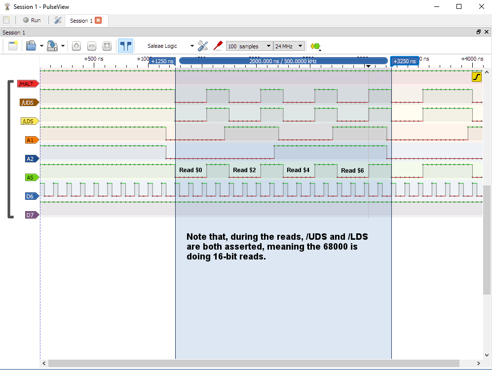
Once I'd realised it was wrong, I went back to the 68000 users manual to check the timings for those initial reads. I also hooked up the logic analyzer to the 68010 to make myself absolutely certain that the chip would actually do the four 16-bit reads I expected after /HALT and /RESET are deasserted. I wanted to double-check this because if it did eight 8-bit reads I'd have to redesign the address decoder to support /UDS and /LDS when /BOOT was asserted.
Thankfully, it looks like it does exactly what I expected (I've annotated the screenshot for clarity):
You'll notice it's actually 16 clock cycles for the four reads (assuming zero wait states). However, this doesn't actually matter - because I know it's four memory cycles, I can simply drive the shift register with the /AS line instead of CLK. Once there have been four cycles, /BOOT will be deasserted and all will be right with the world.
Also, as mentioned in the screenshot, because the initial SSP and PC are fetched with 16-bit reads, I don't need to worry about /UDS and /LDS when /BOOT is low.
So yeah, dodged a bit of a bullet there...
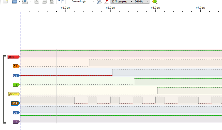
Update: Here is the schematic for the actual circuit that handles the /BOOT line:
And how it looks when analyzed (The important lines here are /AS and /BOOT, the other Qs are the outputs of the intermediate flip-flops I was looking at while debugging a mis-wired connection):
 Ross Bamford
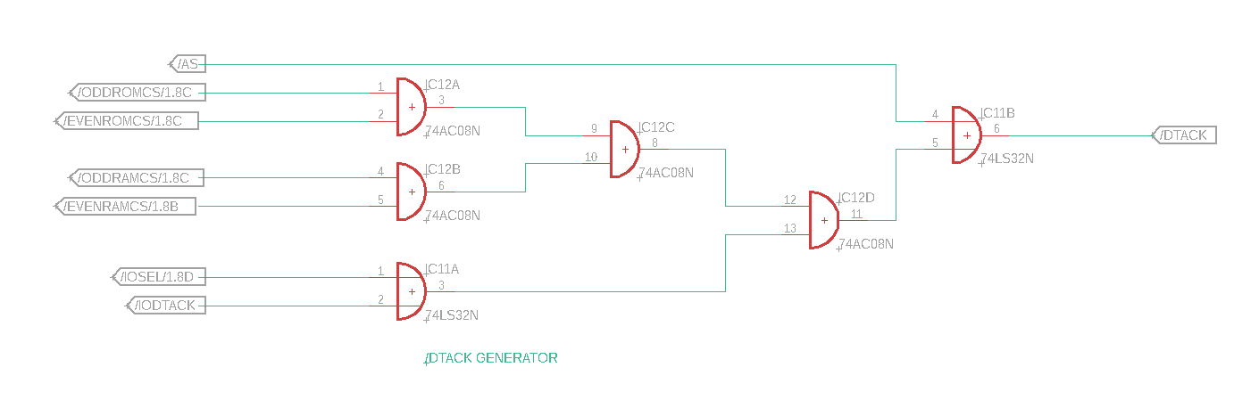
 And here's a trace showing how it looks compared to AS (40n between dots):
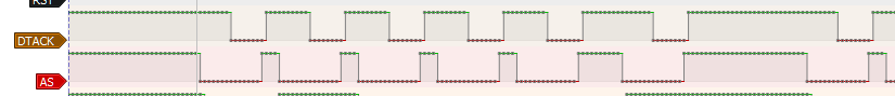 (Good thing I read