Paul Gould
-
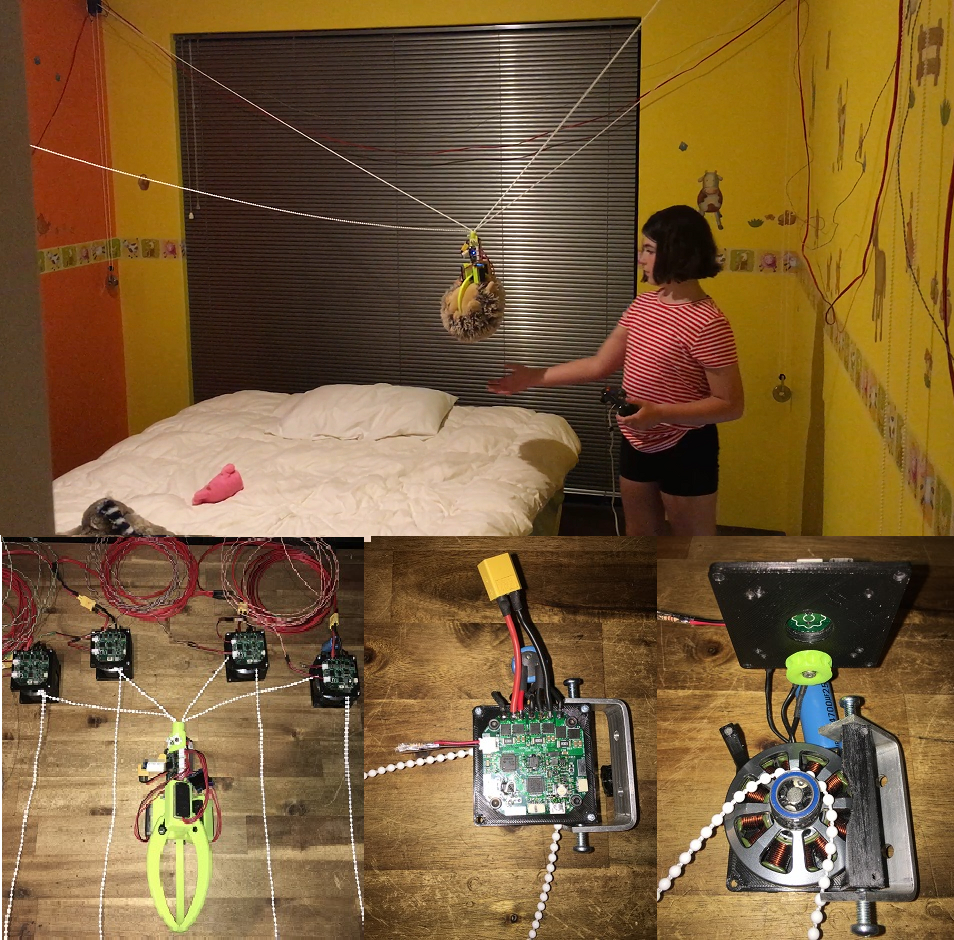
Arcade Claw Machine - Room Sized
08/07/2020 at 10:03 • 0 commentsTHe Brushless Actuators and GL5010 motors are used in Arcade Claw Machine - Room Sized project in the upper four corners of the room. Linked by RS485 communications. Limited to 2% Power.
https://hackaday.io/project/173988-arcade-claw-machine-room-sized
![]()
-
Software for hardware testing
07/05/2020 at 16:05 • 2 comments![]()
Bootloader programmed using the SEGGER J-FLASH with the BIN file from Sparkfun SAMD21 Dev board bootloader. I will have to create my own custom one in the future. This will require using ATMEL studio which I do not like to use.
After bootloader is programmed it can be seen as a USB port in the Arduino IDE. Set the board type to Sparkfun SAMD21 Dev and select the detected USB. The variants file has to be modified to disable the SER5 handler.
Test software runs the following
- Qwiic I2C OLED display
- Reset Button and RX LED
- SerialUSB.read and write
- External SPI magnetic encoder
- On-board SPI magnetic encoder
- EEPROM I2C Read and write
- Free running 6x Sequential ADC via DMA
- DRV8305
- SPI Read and write registers
- Fault and enable
- 3x Current Monitor into ADC
- PWM x3 Mode (not x6 Mode yet)
- RS485 TX and direction (RX not tested yet)
- On-board MOSFET Temperature sensor into ADC
- Battery voltage Monitor into ADC
Features left to test
- Spare UART TX and RX
- RS485 RX
- FAN/Servo PWM output
- External analogue temperature input
Full operation test
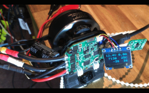
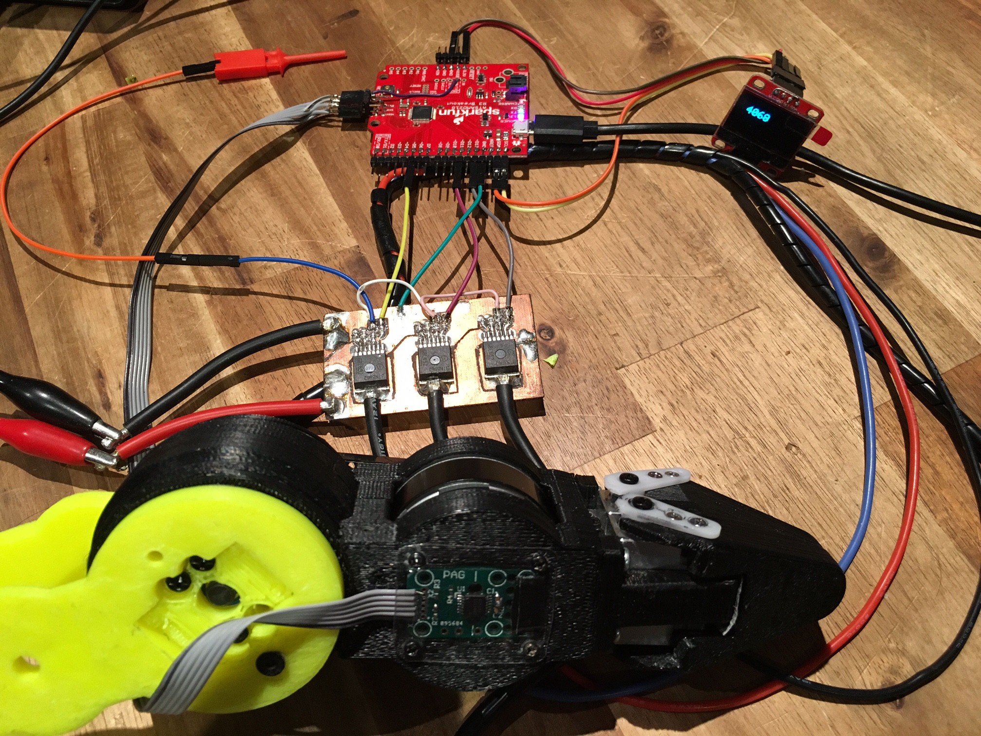
On-board magnetic encoder reads the diametric magnet connected to the motor shaft. Motor position is controlled from the USB using Saddle sinusoidal control. Vital information displayed on the OLED display.
-
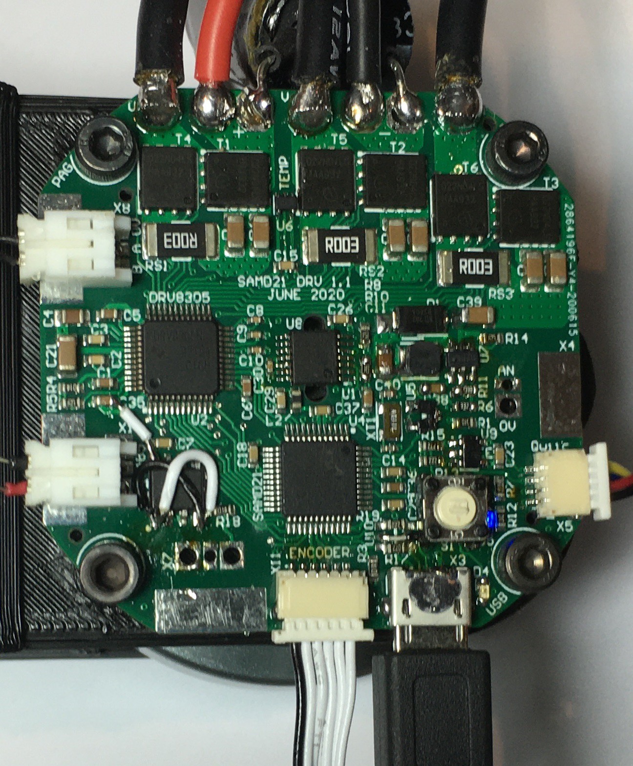
Assembled PCBs
07/05/2020 at 15:29 • 0 comments![]()
Ordered the boards with assembly 18th June 2020 from JLCPCB in China and they arrived in Perth Australia 29th June 2020. There is a limited range of components available, so I had to order the remaining parts, mainly the connectors and sensors, from LSCS and Mouser.
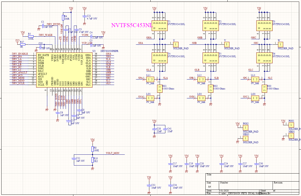
I made a mistake with the polarizing of the diodes because I didn't read the full JLC assembly notes.
I made a mistake with the choice of the SM-regulator and dual power diode. Firstly the reg requires 6V to run the 3.3V supply for the SAMD21. This is fine when running of the external power supply but when operating for the USB this is not good. I reworked the boards with LMR14206 which operates from 4.5V. Which them leads onto the dual power diode. The one I chose has a voltage drop of 1V @ 30mA which is also not good from the USB supply. So a BAT721C can be used as the replacement. It has 0.4V drop at 100mA.
The second mistake was using the DRV8305N which requires a VREG input voltage of 3.3V. I based the design on the DRV83053 which has an internal 3.3V regulator. The '3' cost twice as much at JLC than the 'N'. I just made a link between to the VREG pin from the closest 3.3V pad.
The third mistake was with the pin multiplexing limitation of the RS485 TX and RX pins. These had to be swapped over. This required lifting two pins on the RS485 transceiver chip and adding some wire links.
The fourth mistake was the spacing of the though holes of the fan/servo connector. It was designed for various pitch SMT and TH connectors but a 2.54mm 3pin servo connector wouldn't fit.
-
5 Boards with Assembly are on order at JLC
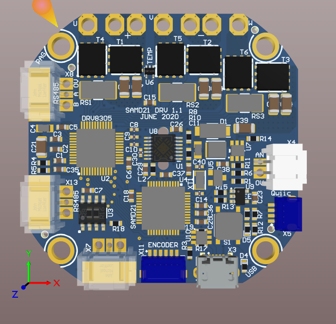
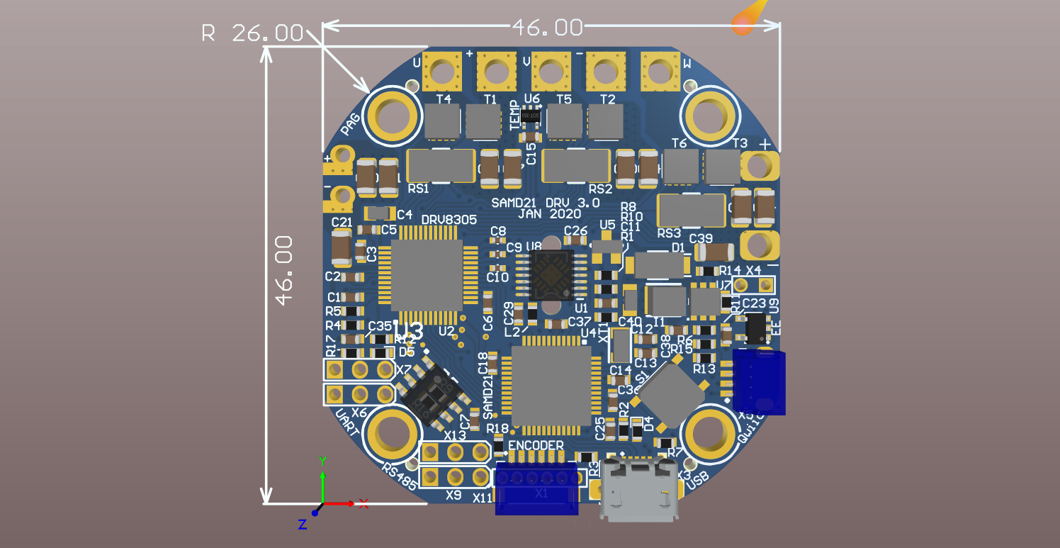
06/14/2020 at 16:19 • 5 commentsSize 50mm square and 58mm round
On board absolute magnetic encoder is either MA730, MA702, AS5147 or AS5047 There are others in this range.
Connectors clockwise from the top
- BLDC motor connectors & Power In/Out
- External Motor Temp
- qwiic
- USB
- Encoder SPI
- Fan or Servo CTRL
- RS485 in/out
- RS485 out/in
The connectors are multi footprint JST. Through hole straight / right angle, SMT straight / right angle
Pitch can be either 1, 1.27, 1.5, 2 or 2.54mm
![]()
Connectors on the back (from the bottom)
- UART TTL
- ISP to load the boot code
- External Capacitor
-
Redesigned for JLC PCB SMT assembly
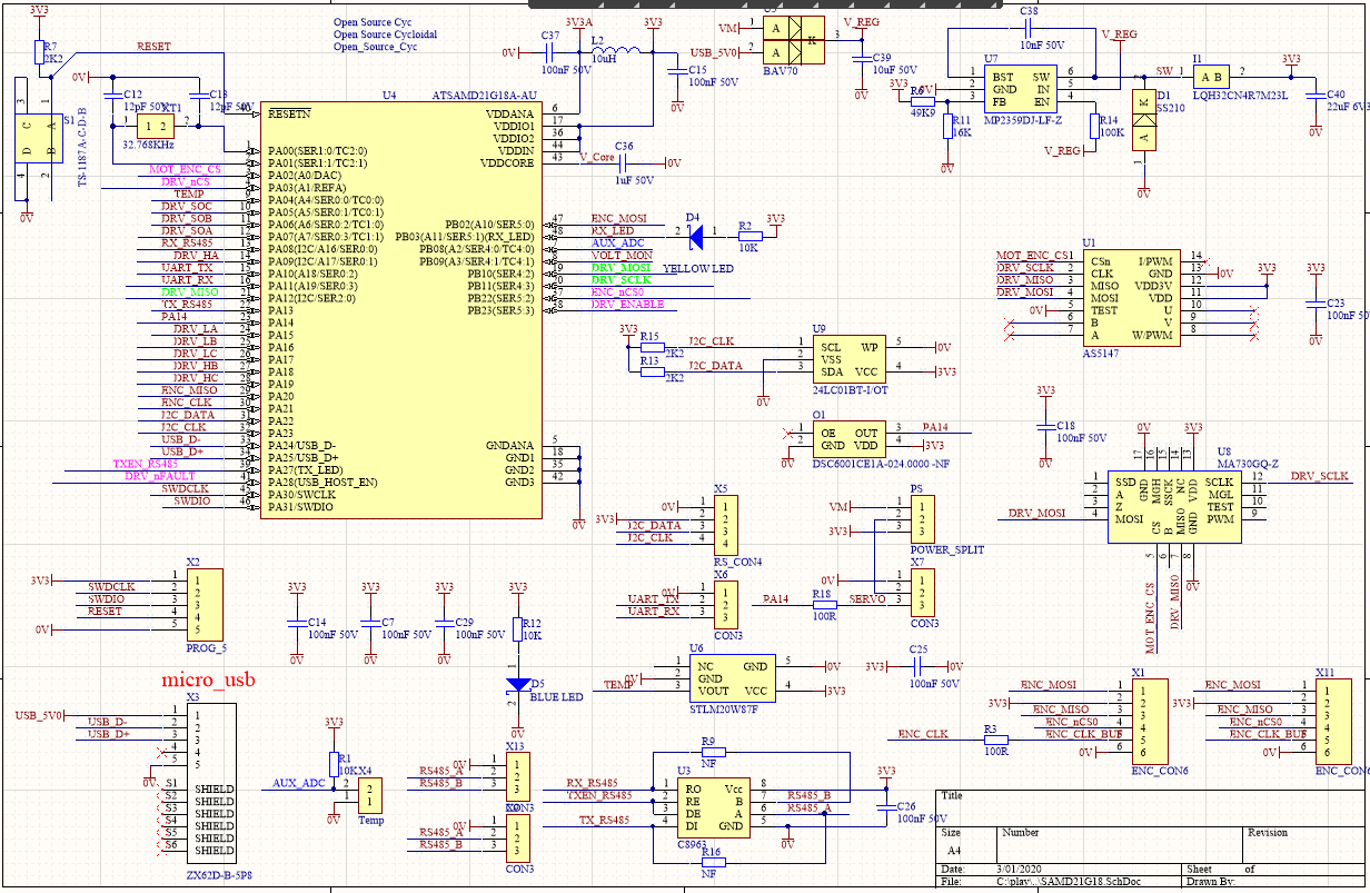
01/03/2020 at 13:14 • 4 commentsJLC now do cheap PCB manufacture and SMT Assembly.
I have changed the components to suit what is available at JLC https://jlcpcb.com/client/index.html#/parts
ATSAMD21G18A-AU (CPU)
DRV8305NPHPR (MOSFET Driver)
with 3 Phase Current Sensor
NVTFS5C453NL (N-MOSFETs 3x3mm 3mOhms 40V)
MA730GQ-Z (Absolute Magnetic Encoder 14-bit SPI) or AS5xxx
MP2359DJ-LF-Z (3V3 1A DC-DC Converter)
SP3485EN-L/TR (RS485 comms)
24LC01BT-I/OT (EEPROM for ID and parameter storage)
STLM20W87F (Temperature Sensor for MOSFETs)
Voltage monitor
External Motor Temperature Connector
Qwiic connector (I2C) for OLED display
SPI Remote Encoder connector
UART Connector
Servo connector
USB programming connector
SWD programming connector (for putting in the Arduino Bootloader
Reset Button (for getting it into the bootloader)
-
The motor is turning
08/21/2019 at 16:42 • 0 comments -
Actuator Operating System - Base Code
08/03/2019 at 16:21 • 0 commentsArduino Code for SAMD21 Dev Breakout by Sparkfun
https://www.sparkfun.com/products/13672?_ga=2.219677657.1904334046.1564414689-1081061511.1562028237
Updated 2019-Aug-05
Fixed DRV SPI CS; Added Test Points T0 & T1; Disabled Serial1
Now on GIT https://github.com/gouldpa/FOC-Arduino-Brushless
Don't use the code below, it will always be out of date
/* External Encoder SPI * Motor Driver Control/Onboard Encoder SPI * 3 Phase timer with deadband TCC0 * Timer IRQ 10KHz Timer 5 * I2C Diaplay * RS485 with time-out Timer 4(start of packet) * ADC sequential, free-running (6) and DMA and IRQ * SerialUSB is available * Serial1 is available but is currently used as test points T0 and T1 * * Joint Control -> PID -> Motor Control (FOC) -> Three Phase Output */ #include <SPI.h> #include "wiring_private.h" // pinPeripheral() function // I2c OLED /////////////////////////////////////////////////////////// #include "ssd1306.h" // library by Alexey Dynda char display_str[] = "1234567890"; // On-Board Encoder + Motor Driver and External Encoder ///////////////// #define ENC_SPI_MISO 6 //29 D6 PA20 ser 5:2 SER #define ENC_SPI_SCK 7 // 30 D7 PA21 ser5:3 SER #define ENC_SPI_MOSI A5 //47 A5 PB02 ser5:0 ALT #define ENC_CS A0 //PA02 #define ENC_CS_PORT_PIN PORT_PA02 // Fast Pin Switching REG_PORT_OUTSET0 SPIClass ENC_SPI_5 (&sercom5, ENC_SPI_MISO, ENC_SPI_SCK, ENC_SPI_MOSI, SPI_PAD_0_SCK_3, SERCOM_RX_PAD_2); #define DRV_SPI_MISO MISO // 21 PA12 SER4:0 ALT #define DRV_SPI_SCK SCK // 20 PB11 SER4:3 ALT #define DRV_SPI_MOSI MOSI //19 PB10 SER4:2 ALT #define DRV_CS 30 // PB22 #define DRV_CS_PORT_PIN PORT_PB22 // Fast Pin Switching USE REG_PORT_OUTSET1 SPIClass DRV_SPI_4 (&sercom4, DRV_SPI_MISO, DRV_SPI_SCK, DRV_SPI_MOSI, SPI_PAD_2_SCK_3, SERCOM_RX_PAD_0); uint16_t enc_data, drv_data; // Three Phase Center Aligned PWM with Dead-band ////////////////// #define UH 3 //W1 14 PA09 #define UL 5 //W5 24 PA15 #define VH 10 //W2 27 PA18 #define VL 11 //W6 25 PA16 #define WH 12 //W3 28 PA19 #define WL 13 //W7 26 PA17 // RS485 Serial with Direction CTRL ///////////////////////////// #define RS485_TX_SIZE 16 #define RS485_RX_SIZE 32 char RS485_txbuf[RS485_TX_SIZE]; char RS485_rxbuf[RS485_RX_SIZE]; #define RS485_RX_MAX 4 #define RS485_TX_PACKET_SIZE 4 #define UART_ERROR 0x80 #define TX_COMPLETE 0x02 #define RX_CHAR 0x04 char RS485_tx_to_send=0; char RS485_tx_left=0; char RS485_rx_cnt=0; uint8_t i=0; #define RS485_RX 38 //PA13 ser2:1 ALT #define RS485_TX 4 //PA08 ser2:0 ALT #define RS485_DIR 2 Uart Serial2 (&sercom2, RS485_RX, RS485_TX, SERCOM_RX_PAD_1, UART_TX_PAD_0); // TC4 serial time-out ////////////////////////////////////////// #define TC4_INTERRUPT 0 //Disable Interrupt // ADC DMA sequential free running (6) with Interrupts ///////////////// #define ADCPIN1 A1 #define ADC_Number 6 #define HWORDS 7 uint16_t adcbuf[HWORDS]; typedef struct { uint16_t btctrl; uint16_t btcnt; uint32_t srcaddr; uint32_t dstaddr; uint32_t descaddr; } dmacdescriptor ; volatile dmacdescriptor wrb[12] __attribute__ ((aligned (16))); dmacdescriptor descriptor_section[12] __attribute__ ((aligned (16))); dmacdescriptor descriptor __attribute__ ((aligned (16))); DmacDescriptor *desc; // DMA descriptor address (so we can change contents) static uint32_t ADC_DMA_chnl = 3; // DMA channel ///// BLDC ////////////////////////////////////////////////////////////////////////////////////// int count; #define SIN_ARRAY_SIZE_BITS 12 #define SIN_ARRAY_SIZE (1<<SIN_ARRAY_SIZE_BITS) #define MOTOR_POLE_PAIRS 7 #define FULL_ANGLE 360.0 #define DEG_RAD (3.1415/180.0) #define FULL_PWM_BITS 10 #define FULL_PWM (1<<FULL_PWM_BITS) #define POS_ONE 0 #define MAGNET_OFFSET -100 //0 #define PHASE_OFFSET 120 #define MAX_PWM 250 /* Store in EEPROM #define CONFIG_ARRAY_SIZE 32 int32 config_array[CONFIG_ARRAY_SIZE]; #define ID_OS 0 #define MAG_OFFSET_OS 1 #define PHASE_OFFSET_OS 2 #define TEMP_MAX_OS 3 #define NOMINAL_OS 4 #define NINETY_OS 5 int current_config = 0; */ int32_t Analog[3]; int32_t servo_val=0; float sin_scale; int phase_offset; int16_t SinArray[SIN_ARRAY_SIZE]; int Temp_Max = 90; int32_t PWMUU; int32_t PWMVV; int32_t PWMWW; int32_t Motor_Position=0; int32_t Motor_Position_Old=0; int32_t Motor_Abs=0; int Motor_Count_Start=0; int32_t Joint_Position; int32_t Tar_Position = 0; int32_t Tar_Position_Speed = 0; int32_t Tar_Speed = 0; int32_t Tar_Move =0; int32_t Motor_Pos_Change=0; int32_t off_set=0; int Kp = 1; int Target_Phase; int8_t Servo_ID=1; unsigned int magnetoffset = 215; unsigned int phase_direction = 0; int phase_set = -115; int32_t Motor_Joint; unsigned int Mag_Sensor_Data; int Motor_on = 0; int incomplete = 1; int time = 0; int forward=0; // common uint32_t counter=0; int start=0; int tpwm=0; #define T0 0 #define T0_PORT PORT_PA10 #define T1 1 #define T1_PORT PORT_PA11 /** * @brief Standard Arduino Setup * @retval void */ void setup() { SerialUSB.begin(115200); //Serial1.begin(115200); Serial2.begin(1000000); // Configure interrupt request NVIC_DisableIRQ(SERCOM2_IRQn); NVIC_ClearPendingIRQ(SERCOM2_IRQn); NVIC_SetPriority(SERCOM2_IRQn, 0); NVIC_EnableIRQ(SERCOM2_IRQn); delay(1000); //Serial1.print("Setup_Sin_array"); /////// Create Sin table based on number of Motor poles Setup_Sin_array(); ENC_SPI_5.begin(); DRV_SPI_4.begin(); pinMode (ENC_CS, OUTPUT); digitalWrite(ENC_CS,HIGH); pinMode (DRV_CS, OUTPUT); digitalWrite(DRV_CS,HIGH); pinPeripheral(ENC_SPI_MISO, PIO_SERCOM); pinPeripheral(ENC_SPI_SCK, PIO_SERCOM); pinPeripheral(ENC_SPI_MOSI, PIO_SERCOM_ALT); pinPeripheral(DRV_SPI_MISO, PIO_SERCOM_ALT); pinPeripheral(DRV_SPI_SCK, PIO_SERCOM_ALT); pinPeripheral(DRV_SPI_MOSI, PIO_SERCOM_ALT); ENC_SPI_5.beginTransaction(SPISettings(1000000, MSBFIRST, SPI_MODE1)); DRV_SPI_4.beginTransaction(SPISettings(1000000, MSBFIRST, SPI_MODE1)); // ADC and DMA adc_init(); dma_init(); // 3 phase TCC0_Setup(); // I2C OLED Display_Init(); // RS_485 pinMode (RS485_DIR, OUTPUT); digitalWrite(RS485_DIR,LOW); pinPeripheral(RS485_RX, PIO_SERCOM); pinPeripheral(RS485_TX, PIO_SERCOM_ALT); // Time-out (Start of Packet) for RS485 TC_Clock_Enable(); TC4_Configure(); //configure the timer TC4_StartCounter(); //starts the timer // 10KHz Timer TC5_Configure(); //configure the timer to run at <sampleRate>Hertz TC5_StartCounter(); //starts the timer pinMode (T0, OUTPUT); digitalWrite(T0,LOW); pinMode (T1, OUTPUT); digitalWrite(T1,LOW); } /** * @brief Standard Arduino Loop * @retval void */ void loop() { Motor_on=1; textDemo(); SerialUSB.print(Target_Phase); SerialUSB.print(' '); SerialUSB.print(Motor_Joint); /* SerialUSB.print(' '); SerialUSB.print(PWMUU); SerialUSB.print(' '); SerialUSB.print(PWMVV); SerialUSB.print(' '); SerialUSB.print(PWMWW); */ SerialUSB.print(' '); SerialUSB.println(Tar_Position); if (SerialUSB.available()) { SerialUSB.read(); if (forward) { Tar_Position=0; forward=0; } else { Tar_Position=8000; forward=1; } } if (0) // Print ADC information { int i; for (i=1; i<7; i++){ SerialUSB.print(adcbuf[i]); SerialUSB.print(" "); } SerialUSB.println(" "); } counter++; if (counter>999){ counter=0;} delay(1); } /** * @brief Puts one variable on the SSD1306 OLED display * @retval void */ static void textDemo() { sprintf(display_str, "%5d ",(drv_data & 0x3FFF) ); ssd1306_setFixedFont(ssd1306xled_font6x8); ssd1306_printFixed2x(0, 16, display_str, STYLE_NORMAL); } /** * @brief this function gets called by the interrupt at 100us or 10kHz * @retval void */ void Task_100us(void) { REG_PORT_OUTSET0 = T1_PORT; REG_PORT_OUTSET0 = T0_PORT; //digitalWrite(1,HIGH); //digitalWrite(0,HIGH); Read_2_Bytes_Dual_SPI(); REG_PORT_OUTCLR0 = T0_PORT; Motor_CTRL(); REG_PORT_OUTSET0 = T0_PORT; Motor_Vector_Phases(Target_Phase, Motor_Joint); REG_PORT_OUTCLR0 = T0_PORT; Three_Phases(); REG_PORT_OUTSET0 = T0_PORT; adc_dma(adcbuf,HWORDS); REG_PORT_OUTCLR0 = T0_PORT; adc_start_with_DMA(); REG_PORT_OUTCLR0 = T1_PORT; } //////////////////////////// BLDC Sub-routines /////////////////////////////////// /* * */ void Three_Phases(void) { if (Motor_on==0) { PWMUU = 0; PWMVV = 0; PWMWW = 0; } REG_TCC0_CCB1 = PWMUU; // TCC0 CCB1 - center the servo on D5 while(TCC0->SYNCBUSY.bit.CCB1); REG_TCC0_CCB2 = PWMVV; // TCC0 CCB2 - center the servo on D6 while(TCC0->SYNCBUSY.bit.CCB2); REG_TCC0_CCB3 = PWMWW; // TCC0 CCB3 - center the servo on D7 while(TCC0->SYNCBUSY.bit.CCB3); } /* * */ void Motor_CTRL(void) { int drive; Motor_Position_Old = Motor_Position; Mag_Sensor_Data = drv_data & 0x3FFF; Motor_Position = (Mag_Sensor_Data>>2); //& 0x2FFF; if (start==0) { start=1; Motor_Abs = 0; } Motor_Pos_Change = (Motor_Position-Motor_Position_Old); if (Motor_Pos_Change>2048) off_set = Motor_Pos_Change-4096; else if (Motor_Pos_Change<-2048) off_set = Motor_Pos_Change + 4096; else off_set = Motor_Pos_Change; Motor_Abs += off_set; Joint_Position = Motor_Abs; // PID Control - Just P for now Motor_Joint = Kp * (Joint_Position - Tar_Position); /* if (forward) Motor_Joint = 250; else Motor_Joint = -250; */ if (Motor_Joint > 0) // Forward or Reverse { drive = PHASE_OFFSET; //phase_set; } else { drive = -PHASE_OFFSET; //phase_set; Motor_Joint = -Motor_Joint; } // Limit Voltage/PWM to motor if (Motor_Joint > MAX_PWM) Motor_Joint = MAX_PWM; // Drive Motor at ~90deg electrically ahead of magnets Target_Phase = Motor_Position + drive + MAGNET_OFFSET; // MAGNET_OFFSET; //Handle wrap-around if (Target_Phase > SIN_ARRAY_SIZE) Target_Phase = Target_Phase - SIN_ARRAY_SIZE; else if (Target_Phase < 0) Target_Phase = Target_Phase + SIN_ARRAY_SIZE; else {} } /* * */ void Motor_Vector_Phases(int Mot_Phase, int Motor_PWM) { int U_Ang = Mot_Phase; int V_Ang = Mot_Phase + phase_offset; int W_Ang = Mot_Phase - phase_offset; if (V_Ang > SIN_ARRAY_SIZE) V_Ang-=SIN_ARRAY_SIZE; if (W_Ang < 0) W_Ang+=SIN_ARRAY_SIZE; PWMUU = (SinArray[U_Ang] * Motor_PWM) >>FULL_PWM_BITS; PWMVV = (SinArray[V_Ang] * Motor_PWM) >>FULL_PWM_BITS; PWMWW = (SinArray[W_Ang] * Motor_PWM) >>FULL_PWM_BITS; } /* * */ void Setup_Sin_array(void) { int step1; float tempa; float tempb; int phase; sin_scale = 1.0/((sin(60*DEG_RAD))+(sin(60*DEG_RAD))); phase_offset = SIN_ARRAY_SIZE/(MOTOR_POLE_PAIRS*3); for (step1=0; step1<SIN_ARRAY_SIZE; step1++) { tempa = (float)step1 / ((float)SIN_ARRAY_SIZE/(float)MOTOR_POLE_PAIRS); phase = floor(tempa); tempb = (tempa-(float)phase) * FULL_ANGLE; if (tempb<(FULL_ANGLE/3.0)) { SinArray[step1] = (int)(( sin((tempb-30.0)* DEG_RAD) - sin((tempb -( 30.0 + 120.0 ))* DEG_RAD) ) * sin_scale * (float)FULL_PWM); } else if (tempb<((FULL_ANGLE*2.0)/3.0)) { SinArray[step1] = (int)(( sin(((240.0-tempb)-30.0)* DEG_RAD) - sin(((240.0-tempb) -( 30.0 + 120.0 ))* DEG_RAD) ) * sin_scale * (float)FULL_PWM); } else { SinArray[step1] = 0; } //Serial1.print(step1); //Serial1.print(','); //Serial1.print(SinArray[step1]); //Serial1.println(); } } /** * @brief Read 2 bytes of SPI on two SPI at the same time * @retval void */ void Read_2_Bytes_Dual_SPI(void) { // It can get stuck in this loop if something goes wrong. // Add some count downs to the while() //digitalWrite(DRV_CS,LOW); // This shouldn't be needed but something is wrong REG_PORT_OUTCLR0 = ENC_CS_PORT_PIN; REG_PORT_OUTCLR1 = DRV_CS_PORT_PIN; //first byte write SERCOM4->SPI.DATA.reg=0xFF; SERCOM5->SPI.DATA.reg=0xFF; while(SERCOM4->SPI.INTFLAG.bit.DRE == 0 ){} //second byte write 4 SERCOM4->SPI.DATA.reg=0xFF; while(SERCOM5->SPI.INTFLAG.bit.DRE == 0 ){} //second byte write 5 SERCOM5->SPI.DATA.reg=0xFF; while(SERCOM4->SPI.INTFLAG.bit.RXC == 0 ){} //first byte read 4 drv_data=(SERCOM4->SPI.DATA.reg)<<8; while(SERCOM5->SPI.INTFLAG.bit.RXC == 0 ){} //first byte read 5 enc_data=(SERCOM5->SPI.DATA.reg)<<8; while(SERCOM4->SPI.INTFLAG.bit.RXC == 0 ){} //second byte read4 drv_data+=SERCOM4->SPI.DATA.reg; while(SERCOM5->SPI.INTFLAG.bit.RXC == 0 ){} //second byte read 5 enc_data+=SERCOM5->SPI.DATA.reg; REG_PORT_OUTSET0 = ENC_CS_PORT_PIN; REG_PORT_OUTSET1 = DRV_CS_PORT_PIN; //digitalWrite(DRV_CS,HIGH); } /** * @brief this function gets called by the interrupt at 100us or 10kHz * @retval void */ void TC5_Handler (void) { Task_100us(); TC5->COUNT16.INTFLAG.bit.MC0 = 1; //don't change this, it's part of the timer code } /* * @brief Initializes TC_Clock_Enable * @retval void */ void TC_Clock_Enable (void) { // Enable GCLK for TCC4 and TC4 (timer counter input clock) GCLK->CLKCTRL.reg = (uint16_t) (GCLK_CLKCTRL_CLKEN | GCLK_CLKCTRL_GEN_GCLK0 | GCLK_CLKCTRL_ID(GCM_TC4_TC5)) ; while (GCLK->STATUS.bit.SYNCBUSY); } /** * @brief Initializes TC5_Configure * @param int sampleRate * @retval void */ void TC5_Configure() { //reset timer TC5->COUNT16.CTRLA.reg = TC_CTRLA_SWRST; while (TC5->COUNT16.STATUS.reg & TC_STATUS_SYNCBUSY); while (TC5->COUNT16.CTRLA.bit.SWRST); // Set Timer counter Mode to 16 bits TC5->COUNT16.CTRLA.reg |= TC_CTRLA_MODE_COUNT16; // Set TC5 mode as match frequency TC5->COUNT16.CTRLA.reg |= TC_CTRLA_WAVEGEN_MFRQ; //set prescaler and enable TC5 TC5->COUNT16.CTRLA.reg |= TC_CTRLA_PRESCALER_DIV1 | TC_CTRLA_ENABLE; //set TC5 timer counter based off of the system clock and the user defined sample rate or waveform TC5->COUNT16.CC[0].reg = (uint16_t) 4800; while (TC5->COUNT16.STATUS.reg & TC_STATUS_SYNCBUSY); // Configure interrupt request NVIC_DisableIRQ(TC5_IRQn); NVIC_ClearPendingIRQ(TC5_IRQn); NVIC_SetPriority(TC5_IRQn, 7); // 0 is the highest Priority Interrupt; RS485 should be the highest NVIC_EnableIRQ(TC5_IRQn); // Enable the TC5 interrupt request TC5->COUNT16.INTENSET.bit.MC0 = 1; while (TC5->COUNT16.STATUS.reg & TC_STATUS_SYNCBUSY); //wait until TC5 is done syncing } /** * @brief Starts/Enables TC5_StartCounter and waits for it to be ready * @retval void */ void TC5_StartCounter() { TC5->COUNT16.CTRLA.reg |= TC_CTRLA_ENABLE; //set the CTRLA register while (TC5->COUNT16.STATUS.reg & TC_STATUS_SYNCBUSY); //wait until snyc'd } /** * @brief disable TC5 * @retval void */ void TC5_Disable() { TC5->COUNT16.CTRLA.reg &= ~TC_CTRLA_ENABLE; while (TC5->COUNT16.STATUS.reg & TC_STATUS_SYNCBUSY); } /** * @brief Initialation Timer TCC0 * @retval void */ void TCC0_Setup() { REG_GCLK_GENDIV = GCLK_GENDIV_DIV(2) | // Divide the 48MHz clock source by divisor 3: 48MHz/3=16MHz GCLK_GENDIV_ID(4); // Select Generic Clock (GCLK) 4 while (GCLK->STATUS.bit.SYNCBUSY); // Wait for synchronization REG_GCLK_GENCTRL = GCLK_GENCTRL_IDC | // Set the duty cycle to 50/50 HIGH/LOW GCLK_GENCTRL_GENEN | // Enable GCLK4 GCLK_GENCTRL_SRC_DFLL48M | // Set the 48MHz clock source GCLK_GENCTRL_ID(4); // Select GCLK4 while (GCLK->STATUS.bit.SYNCBUSY); // Wait for synchronization // Enable the port multiplexer for the 3 PWM channels: timer TCC0 outputs const uint8_t CHANNELS = 6; const uint8_t pwmPins[] = { UH, UL, VH, VL, WH, WL }; for (uint8_t i = 0; i < CHANNELS; i++) { PORT->Group[g_APinDescription[pwmPins[i]].ulPort].PINCFG[g_APinDescription[pwmPins[i]].ulPin].bit.PMUXEN = 1; } // Connect the TCC0 timer to the port outputs - port pins are paired odd PMUO and even PMUXE // F & E specify the timers: TCC0, TCC1 and TCC2 PORT->Group[g_APinDescription[UH].ulPort].PMUX[g_APinDescription[UH].ulPin >> 1].reg = PORT_PMUX_PMUXO_E | PORT_PMUX_PMUXE_F; //W1 14 PA09 PORT->Group[g_APinDescription[UL].ulPort].PMUX[g_APinDescription[UL].ulPin >> 1].reg = PORT_PMUX_PMUXO_F | PORT_PMUX_PMUXE_F; //W5 24 PA15 PORT->Group[g_APinDescription[VH].ulPort].PMUX[g_APinDescription[VH].ulPin >> 1].reg = PORT_PMUX_PMUXO_F | PORT_PMUX_PMUXE_F; //W2 27 PA18 PORT->Group[g_APinDescription[VL].ulPort].PMUX[g_APinDescription[VL].ulPin >> 1].reg = PORT_PMUX_PMUXO_F | PORT_PMUX_PMUXE_F; //W6 25 PA16 PORT->Group[g_APinDescription[WH].ulPort].PMUX[g_APinDescription[WH].ulPin >> 1].reg = PORT_PMUX_PMUXO_F | PORT_PMUX_PMUXE_F; //W3 28 PA19 PORT->Group[g_APinDescription[WL].ulPort].PMUX[g_APinDescription[WL].ulPin >> 1].reg = PORT_PMUX_PMUXO_F | PORT_PMUX_PMUXE_F; //W7 26 PA17 // Feed GCLK4 to TCC0 and TCC1 REG_GCLK_CLKCTRL = GCLK_CLKCTRL_CLKEN | // Enable GCLK4 to TCC0 and TCC1 GCLK_CLKCTRL_GEN_GCLK4 | // Select GCLK4 GCLK_CLKCTRL_ID_TCC0_TCC1; // Feed GCLK4 to TCC0 and TCC1 while (GCLK->STATUS.bit.SYNCBUSY); // Wait for synchronization // Dual slope PWM operation: timers countinuously count up to PER register value then down 0 //REG_TCC0_WAVE |= TCC_WAVE_POL(0xF) | TCC_WAVE_WAVEGEN_DSBOTTOM; // Reverse the output polarity on all TCC0 outputs // Setup dual slope PWM on TCC0 REG_TCC0_WAVE |= TCC_WAVE_WAVEGEN_DSBOTTOM; // Reverse the output polarity on all TCC0 outputs // Setup dual slope PWM on TCC0 while (TCC0->SYNCBUSY.bit.WAVE); // Wait for synchronization // Each timer counts up to a maximum or TOP value set by the PER register, // this determines the frequency of the PWM operation: // 20000 = 50Hz, 10000 = 100Hz, 2500 = 400Hz REG_TCC0_PER = 1000; // Set the frequency of the PWM on TCC0 to 50Hz while(TCC0->SYNCBUSY.bit.PER); // The CCBx register value corresponds to the pulsewidth in microseconds (us) REG_TCC0_CCB1 = 500; // TCC0 CCB1 - center the servo on D5 while(TCC0->SYNCBUSY.bit.CCB1); REG_TCC0_CCB2 = 300; // TCC0 CCB2 - center the servo on D6 while(TCC0->SYNCBUSY.bit.CCB2); REG_TCC0_CCB3 = 100; // TCC0 CCB3 - center the servo on D7 while(TCC0->SYNCBUSY.bit.CCB3); // Set the output matrix so that D3 and D7 are set to output CC0 and enable low and high dead time insertion REG_TCC0_WEXCTRL |= TCC_WEXCTRL_DTHS(5) | TCC_WEXCTRL_DTLS(5) | TCC_WEXCTRL_DTIEN3 | TCC_WEXCTRL_DTIEN2 | TCC_WEXCTRL_DTIEN1; // | TCC_WEXCTRL_OTMX(0x2); while(TCC0->SYNCBUSY.bit.CCB2); REG_TCC0_DRVCTRL |= TCC_DRVCTRL_INVEN3 | TCC_DRVCTRL_INVEN2 | TCC_DRVCTRL_INVEN1; while(TCC0->SYNCBUSY.bit.CCB2); // Divide the 16MHz signal by 8 giving 2MHz (0.5us) TCC0 timer tick and enable the outputs //REG_TCC0_CTRLA |= TCC_CTRLA_PRESCALER_DIV1 | TCC_CTRLA_ENABLE; // Divide GCLK4 by 8, Enable the TCC0 output REG_TCC0_CTRLA |= TCC_CTRLA_PRESCALER_DIV1 | TCC_CTRLA_ENABLE; // Divide GCLK4 by 8, Enable the TCC0 output while (TCC0->SYNCBUSY.bit.ENABLE); // Wait for synchronization } /** * @brief Initialization for the SSD1306 OLED display via I2C * @retval void */ void Display_Init() { ssd1306_setFixedFont(ssd1306xled_font6x8); ssd1306_128x64_i2c_init(); ssd1306_clearScreen(); } /* * @brief TX and RX Interrupt * @param * @retval void */ void SERCOM2_Handler() { char flag = SERCOM2->USART.INTFLAG.reg; int uart_status; if (flag & TX_COMPLETE){ // TX Complete if (RS485_tx_left){ SERCOM2->USART.DATA.reg = RS485_txbuf[RS485_tx_to_send-RS485_tx_left]; SERCOM2->USART.INTENCLR.reg = 0x01; SERCOM2->USART.INTENSET.reg = 0x86; SERCOM2->USART.INTFLAG.reg = TX_COMPLETE; RS485_tx_left--; } else{ SERCOM2->USART.INTENCLR.reg = 0x00; SERCOM2->USART.INTENSET.reg = 0x84; SERCOM2->USART.INTFLAG.reg = TX_COMPLETE; digitalWrite(RS485_DIR,LOW); } } if (flag & RX_CHAR){ // RX in if (TC4->COUNT16.COUNT.reg>100) //Check if this is a new packet (using timeout) { RS485_rx_cnt=0; } TC4->COUNT16.COUNT.reg=0; //Reset the timeout RS485_rxbuf[RS485_rx_cnt] = SERCOM2->USART.DATA.reg; // Put new byte into packet SERCOM2->USART.INTENSET.reg = 0x84; if (RS485_rx_cnt ==(RS485_RX_MAX-1)) // if the packet is complete reply [other checks required] { //parse the rx packet; Full Packet Received Serial2_Transmit(RS485_TX_PACKET_SIZE); // Send a reply } RS485_rx_cnt++; } if (flag & UART_ERROR){ uart_status = SERCOM2->USART.STATUS.reg; SERCOM2->USART.STATUS.reg = uart_status; SERCOM2->USART.INTENSET.reg = 0x86; SERCOM2->USART.INTENCLR.reg = 0x80; SERCOM2->USART.INTFLAG.reg = UART_ERROR; } } /* * @brief Sends RS485 packet * @param int RS485_chars_to_send * @retval void */ void Serial2_Transmit(int RS485_chars_to_send){ digitalWrite(RS485_DIR,HIGH); //Set RS485 Transceiver to Transmit //delayMicroseconds(1); // Create Packet to send int p; for (p=0; p<RS485_TX_SIZE; p++) { RS485_txbuf[p]=p; } RS485_tx_left = RS485_chars_to_send; RS485_tx_to_send = RS485_chars_to_send; SERCOM2->USART.DATA.reg = RS485_txbuf[RS485_tx_to_send -RS485_tx_left]; SERCOM2->USART.INTENSET.reg = 0x86; RS485_tx_left--; } /* * @brief Initializes TC4_Handler * @retval void */ void TC4_Handler (void) { TC4->COUNT16.INTFLAG.bit.MC0 = 1; //don't change this, it's part of the timer code } /* * @brief Initializes TC4_Configure * @retval void */ void TC4_Configure(void) { //reset timer TC4->COUNT16.CTRLA.reg = TC_CTRLA_SWRST; while (TC4->COUNT16.STATUS.reg & TC_STATUS_SYNCBUSY); while (TC4->COUNT16.CTRLA.bit.SWRST); // Set Timer counter Mode to 16 bits TC4->COUNT16.CTRLA.reg |= TC_CTRLA_MODE_COUNT16; // Set TC4 mode as match frequency TC4->COUNT16.CTRLA.reg |= TC_CTRLA_WAVEGEN_MFRQ; //set prescaler and enable TC4 TC4->COUNT16.CTRLA.reg |= TC_CTRLA_PRESCALER_DIV256 | TC_CTRLA_ENABLE; TC4->COUNT16.CTRLBCLR.reg |= TC_CTRLBCLR_DIR; //set TC4 timer counter based off of the system clock and the user defined sample rate or waveform TC4->COUNT16.CC[0].reg = 10000; while (TC4->COUNT16.STATUS.reg & TC_STATUS_SYNCBUSY); if (TC4_INTERRUPT) { // Configure interrupt request NVIC_DisableIRQ(TC4_IRQn); NVIC_ClearPendingIRQ(TC4_IRQn); NVIC_SetPriority(TC4_IRQn, 7); NVIC_EnableIRQ(TC4_IRQn); // Enable the TC4 interrupt request TC4->COUNT16.INTENSET.bit.MC0 = 1; while (TC4->COUNT16.STATUS.reg & TC_STATUS_SYNCBUSY); //wait until TC5 is done syncing } } /** * @brief Starts/Enables TC4_StartCounter and waits for it to be ready * @retval void */ void TC4_StartCounter() { TC4->COUNT16.CTRLA.reg |= TC_CTRLA_ENABLE; //set the CTRLA register while (TC4->COUNT16.STATUS.reg & TC_STATUS_SYNCBUSY); //wait until snyc'd } /** * @brief disable TC4 * @retval void */ void TC4_Disable() { TC4->COUNT16.CTRLA.reg &= ~TC_CTRLA_ENABLE; while (TC4->COUNT16.STATUS.reg & TC_STATUS_SYNCBUSY); } /** * @brief dma_init * @retval void */ void dma_init() { // probably on by default PM->AHBMASK.reg |= PM_AHBMASK_DMAC ; PM->APBBMASK.reg |= PM_APBBMASK_DMAC ; NVIC_EnableIRQ( DMAC_IRQn ) ; DMAC->BASEADDR.reg = (uint32_t)descriptor_section; DMAC->WRBADDR.reg = (uint32_t)wrb; DMAC->CTRL.reg = DMAC_CTRL_DMAENABLE | DMAC_CTRL_LVLEN(0xf); } /** * @brief adc_dma * @retval void */ void adc_dma(void *rxdata, size_t hwords) { uint32_t temp_CHCTRLB_reg; DMAC->CHID.reg = DMAC_CHID_ID(ADC_DMA_chnl); DMAC->CHCTRLA.reg &= ~DMAC_CHCTRLA_ENABLE; DMAC->CHCTRLA.reg = DMAC_CHCTRLA_SWRST; DMAC->SWTRIGCTRL.reg &= (uint32_t)(~(1 << ADC_DMA_chnl)); temp_CHCTRLB_reg = DMAC_CHCTRLB_LVL(0) | DMAC_CHCTRLB_TRIGSRC(ADC_DMAC_ID_RESRDY) | DMAC_CHCTRLB_TRIGACT_BEAT; DMAC->CHCTRLB.reg = temp_CHCTRLB_reg; DMAC->CHINTENSET.reg = DMAC_CHINTENSET_MASK ; // enable all 3 interrupts descriptor.descaddr = 0; descriptor.srcaddr = (uint32_t) &ADC->RESULT.reg; descriptor.btcnt = hwords; descriptor.dstaddr = (uint32_t)rxdata + hwords*2; // end address descriptor.btctrl = DMAC_BTCTRL_BEATSIZE_HWORD | DMAC_BTCTRL_DSTINC | DMAC_BTCTRL_VALID; memcpy(&descriptor_section[ADC_DMA_chnl],&descriptor, sizeof(dmacdescriptor)); // start channel DMAC->CHID.reg = DMAC_CHID_ID(ADC_DMA_chnl); DMAC->CHCTRLA.reg |= DMAC_CHCTRLA_ENABLE; } /** * @brief ADC sync wait * @retval void */ static __inline__ void ADCsync() __attribute__((always_inline, unused)); static void ADCsync() { while (ADC->STATUS.bit.SYNCBUSY == 1); //Just wait till the ADC is free } /** * @brief Initialize ADC * @retval void */ void adc_init(){ analogRead(ADCPIN1); // do some pin init pinPeripheral() ADC->CTRLA.bit.ENABLE = 0x00; // Disable ADC ADCsync(); //ADC->REFCTRL.bit.REFSEL = ADC_REFCTRL_REFSEL_INTVCC0_Val; // 2.2297 V Supply VDDANA //ADC->INPUTCTRL.bit.GAIN = ADC_INPUTCTRL_GAIN_1X_Val; // Gain select as 1X ADC->INPUTCTRL.bit.GAIN = ADC_INPUTCTRL_GAIN_DIV2_Val; // default ADC->REFCTRL.bit.REFSEL = ADC_REFCTRL_REFSEL_INTVCC1_Val; ADCsync(); // ref 31.6.16 ADC->INPUTCTRL.bit.MUXPOS = 1; ADCsync(); ADC->INPUTCTRL.bit.INPUTSCAN = ADC_Number+1; ADCsync(); ADC->INPUTCTRL.bit.INPUTOFFSET = 0; ADCsync(); ADC->AVGCTRL.reg = 0x00 ; //no averaging ADC->SAMPCTRL.reg = 0x05; ; //sample length in 1/2 CLK_ADC cycles ADCsync(); ADC->CTRLB.reg = ADC_CTRLB_PRESCALER_DIV16 | ADC_CTRLB_FREERUN | ADC_CTRLB_RESSEL_12BIT; ADCsync(); } /** * @brief adc_stop_with_DMA * @retval void */ void adc_stop_with_DMA(void) { ADC->CTRLA.bit.ENABLE = 0x00; } /** * @brief adc_start_with_DMA * @retval void */ void adc_start_with_DMA(void) { ADC->INPUTCTRL.bit.MUXPOS = 1; ADC->INPUTCTRL.bit.INPUTSCAN = ADC_Number+1; ADC->INPUTCTRL.bit.INPUTOFFSET = 0; ADC->SWTRIG.bit.FLUSH = 1; ADC->CTRLA.bit.ENABLE = 0x01; } /** * @brief DMAC_Handler * @retval void */ void DMAC_Handler() { uint8_t active_channel; active_channel = DMAC->INTPEND.reg & DMAC_INTPEND_ID_Msk; // get channel number DMAC->CHID.reg = DMAC_CHID_ID(active_channel); adc_stop_with_DMA(); DMAC->CHINTFLAG.reg = DMAC_CHINTENCLR_TCMPL; // clear DMAC->CHINTFLAG.reg = DMAC_CHINTENCLR_TERR; DMAC->CHINTFLAG.reg = DMAC_CHINTENCLR_SUSP; } /* MIT License Copyright (c) 2017-2019, Alexey Dynda Permission is hereby granted, free of charge, to any person obtaining a copy of this software and associated documentation files (the "Software"), to deal in the Software without restriction, including without limitation the rights to use, copy, modify, merge, publish, distribute, sublicense, and/or sell copies of the Software, and to permit persons to whom the Software is furnished to do so, subject to the following conditions: The above copyright notice and this permission notice shall be included in all copies or substantial portions of the Software. THE SOFTWARE IS PROVIDED "AS IS", WITHOUT WARRANTY OF ANY KIND, EXPRESS OR IMPLIED, INCLUDING BUT NOT LIMITED TO THE WARRANTIES OF MERCHANTABILITY, FITNESS FOR A PARTICULAR PURPOSE AND NONINFRINGEMENT. IN NO EVENT SHALL THE AUTHORS OR COPYRIGHT HOLDERS BE LIABLE FOR ANY CLAIM, DAMAGES OR OTHER LIABILITY, WHETHER IN AN ACTION OF CONTRACT, TORT OR OTHERWISE, ARISING FROM, OUT OF OR IN CONNECTION WITH THE SOFTWARE OR THE USE OR OTHER DEALINGS IN THE SOFTWARE. */ -
Software tasks
04/30/2019 at 16:44 • 0 commentsLow Level SAMD21 / Arduino functions with no libraries*
- Main OS timer - 100us (10KHz) IRQ (done)
- 3-Phase Motor Controller PWM with deadband (done)
- (6-centre aligned pwms) (done)
- ADC- 6 channels sequential, semi-free-running DMA with IRQ (done)
- 3x Current Sensor
- MOSFET Temperature Sensor
- Battery Voltage
- 1 Auxillary Analog Inputs
- Dual (same time) SPI (blocking and IRQ) (done)
- RS485 UART with IRQ (TX & RX) (done)
- with direction CTRL (done)
- with time-out and packet start detect (done)
- UART with DMA (attempted & fail)
- CPU's Internal EEPROM Emulation (Flash storage) (attempted & fail)
- External I2C EEPROM support (maybe Libraries) (not started, have eeprom)
- I2C OLED support (with Libraries) (done)
- SerialUSB with above (done)
- Serial1 with above (done)
- Making all the Low level features work together (done, done and done)
High Level Functions
- Field Orientated Control (FOC) & Motor Commutation (done)
- PID Joint Control (done, but just P)
- RS485 Packet Structure (1/2 done)
- MOSFET Driver configuration (To be ported from PSOC4)
- Motor Position and other configuration (simple position control)
Brushless Actuator (Arduino-Compatible)
Ardunio-Compatible M0/Zero/SAMD21 with FET Driver, MOSFETs, Absolute Magnetic Encoder, USB and RS485 comms. ~$US50