This experiment is an attempt to connect an NEC V20 chip to an FPGA board. This is inspired by a few of the webpages I've read :
- https://suchprogramming.com/fpga-meets-6502/
- http://www.homebrew8088.com/
- https://helmpcb.com/electronics/8088-computer
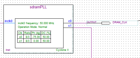
Initially, I had planned to connect the V20 to the supporting logic chips for memory decoding and etc., but it could be an extremely difficult approach as many things could go wrong in between. In order to save time, I directly connect this V20 to the FPGA board I have. Lucky for me, this FPGA board has a 32MB SDRAM which I could load up a small BIOS inside and as a frame buffer for the video generator.
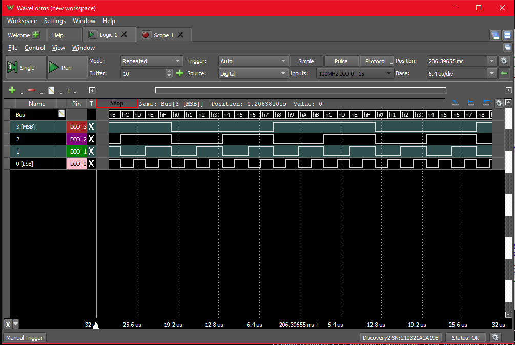
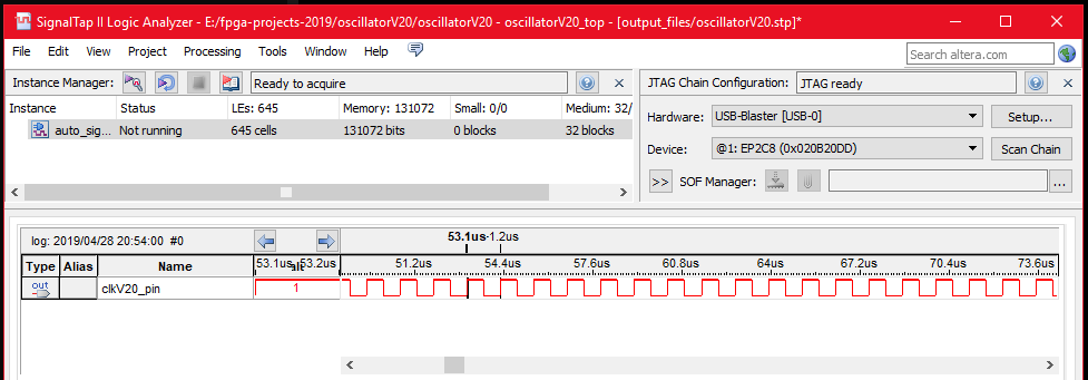
As a start, some of the experiment will be done in SignalTap II to verify the operations of the decoders are correct or not.
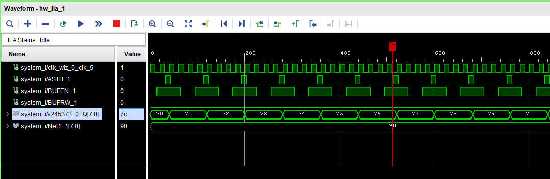
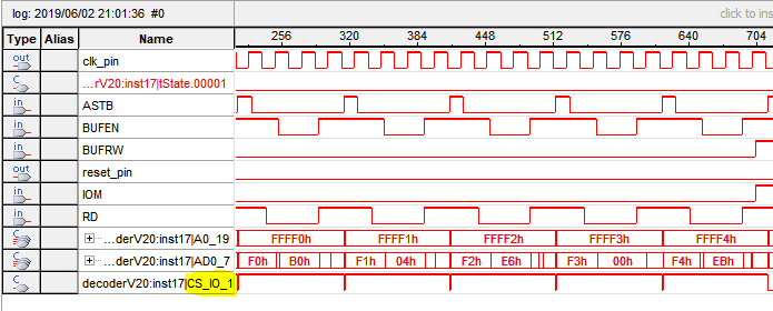
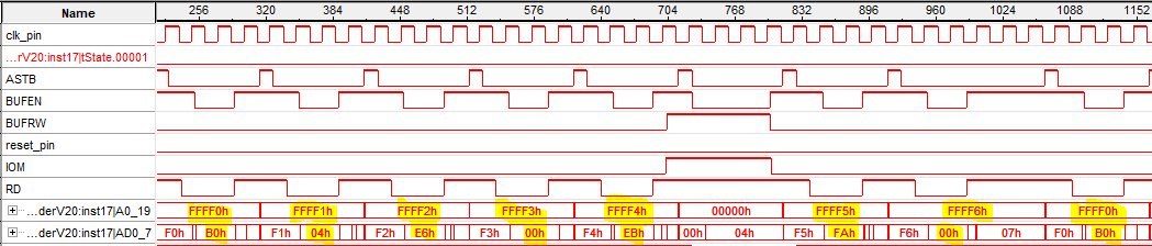
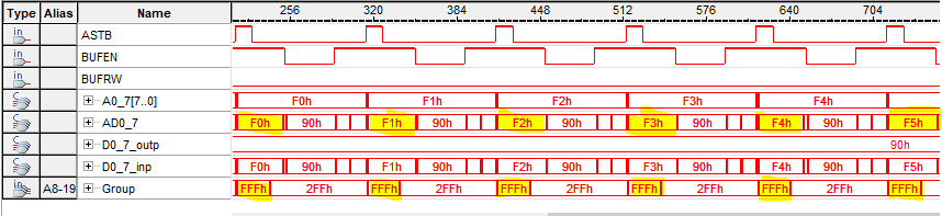
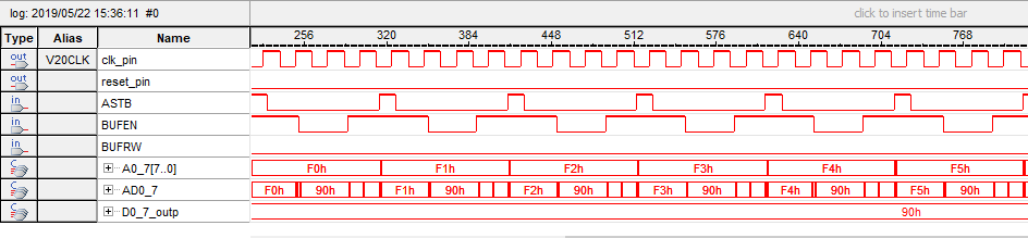
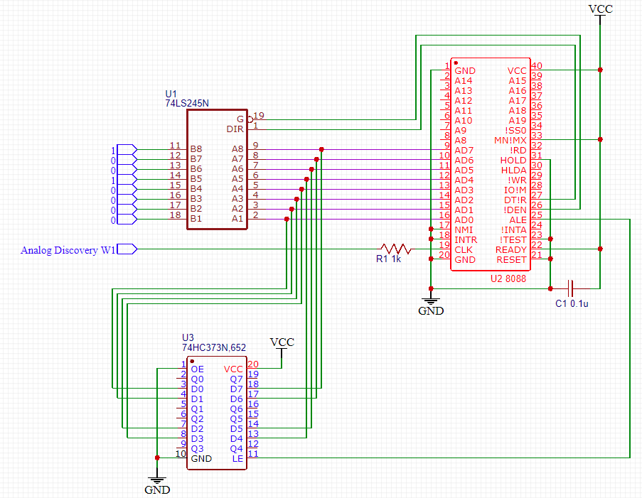
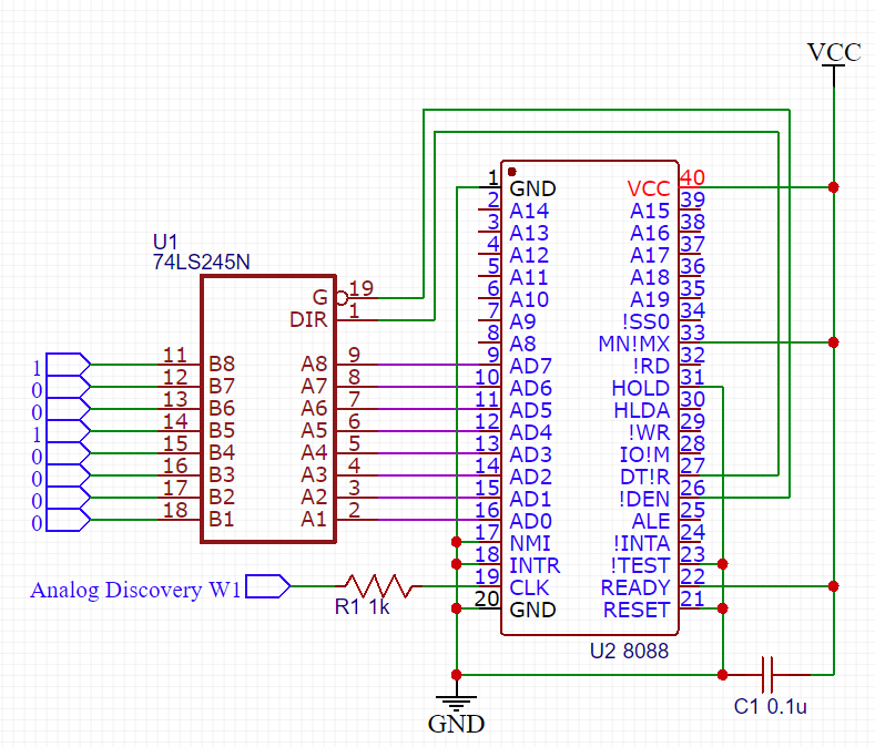


Yes, on-chip resources for latch are available on any FPGA - however, trying to write it in Verilog is an extremely tricky task. I couldn't have this FPGA grabbing that lower address from AD0-7 at the first cycle despite following the "inout" examples online. I might have left out something, or I might need to look harder!
So to have all the basic stuff working, I will have to add that 373 on top of it, and fully isolate all the address and the data so that the FPGA can work on its decoding and mapping (which is my main intention) to different peripherals and the memory.