John Lonergan
-
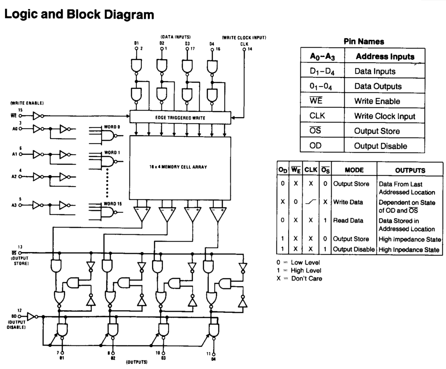
Playing with the DM85S68 16x4 synchronous register file
07/25/2020 at 23:19 • 0 commentsThe DM85S68 is an oldie. I came across it when researching register files for SPAM1 and when I bought a few 74HCT670's I also bought a few DM85S68 too (at least I hope they're not counterfeit).
Unlike the 74HCT670, which is entirely asynchronous, the DM85S68 has a synchronous load and an async read. This means it's probably better suited to my needs than the 74HCT670. Where I've designed around the 670 I've had to add a 74HCT574 to latch the data input because without this then the register file and the ALU would be a big combinatorial circuit with a feedback loop; not good.
Also, the 74670 is a 4x4 register, vs the 16x4 DM85S68, so whilst I'm only building 4 registers then that's immaterial, but if I went for the full 8 registers my addressing permits at the moment then perhaps the DM85S68 is a better choice.
The big downside perhaps of the DM85S68 is that it's supply current is rated as 70mA typical compared to the 74HCT670 which will use a fraction of that.
The logic diagram is shown below and you can see that the output stage is interesting in that it contains a latch.
The output latch appears to be some kind of SR latch. I also had a go at simulating it CircuitVerse and also in Falsted.
I won't use DM85S68 immediately as I'd need to create a verilog model for it - but it's definitely on the todo list for a variation.
You can find the DM85S68 datasheet here
https://www.datasheetarchive.com/pdf/download.php?id=96fbc3fe56bdaed595c8bb5f81c37e1b016adc&type=M&term=DM85S68 and also some original design ideas in this old data book http://www.bitsavers.org/components/national/_dataBooks/1978_National_Memory_Applications_Handbook.pdf
-
ALU Design finally completed and tested
07/25/2020 at 23:01 • 0 commentsI finally got to the end of desiging the ALU - the result is documented here https://github.com/Johnlon/spam-1/blob/master/docs/alu_with_carry_in.md
0-7 ALU Ops 8-15 ALU Ops 16-23 ALU Ops 24-31 ALU Ops 0 B-1 A*B (high bits) A RRC B A A+B*1 A*B (low bits) A AND B B A-B*1 A/B A OR B -A B-A*1 A%B A XOR B -B A-B (special) A << B A NAND B BA / 10 A+B+1*2 A >> B arithmetic NOT B BA % 10 A-B-1*2 A >> B logical A+B (BCD) B+1 B-A-1*2 A RLC B A-B (BCD) This ALU is based on Warren Toomey's ALU for CscVon8 but with a few significant differences that are detailed in the ALU design page for SPAM-1.
There is a verilog implementation of the ALU https://github.com/Johnlon/spam-1/blob/master/verilog/alu/alu_code.v and a bunch of unit tests for each operation https://github.com/Johnlon/spam-1/blob/master/verilog/alu/test.v.
Once I had that passing I needed to generated an image file for burning a ROM and also because I wanted to use the same data file to drive an alternative impl using a verilog ROM loaded from that datafile so that I could run the CPU and unit test against it.
The approach I took was to create the data file by writing a small verilog program that applied all possible input values to the verilog ALU implentation and then writing the inputs and outputs to disk as a ROM image.
The program was pretty simple https://github.com/Johnlon/spam-1/blob/master/verilog/alu/gen_alu.v and generated all the files I need to create some physical ROMS when I get to the H/W build - which will be as soon as I can clear a space at home to start work.
-
Single Cycle CPU Confusion
07/19/2020 at 23:53 • 0 commentsI was writing up some design/research notes on timing considerations and I was considering whether it was possible to update async RAM in a single cycle.
I have heard the term "Single Cycle Cpu" and was trying to understand what single cycle cpu actually meant. Is there a clear definition and consensus and what is means?
The home brew "single cycle cpu's" I've come across seem to use both the rising and the falling edges of the clock to complete a single instruction. Typically, the rising edge acts as fetch/decode and the falling edge as execute.
However, in my reading I came across the reasonable point made here ... https://zipcpu.com/blog/2017/08/21/rules-for-newbies.html
"Do not transition on any negative (falling) edges. Falling edge clocks should be considered a violation of the one clock principle, as they act like separate clocks.".
This rings true to me. Changing state on the rising and falling edges (or high and low phases) is effectively the same as changing state on the rising edge of two cycles of a clock that's running twice as fast; and this would be a "two cycle" CPU wouldn't it.
So is it honest to state that a design is a single cycle CPU when both the rising and falling edges are actively used for state change?
It would seem that a true single cycle cpu must perform all state changing operations on a single clock edge of a single clock cycle.
I can imagine such a thing is possible providing the data strorage is all synchronous. If we have a synchronous system that has settled then on the next clock edge we can clock the results into a synchronous data store and simultaneously clock the program counter on to the next address. But if the data store is async then the control lines would be changing whilst that data is being stored leading to unintended behaviours.
Am I wrong, are there any examples of such that include async storage in the mix?
It would seem that using async RAM in ones design means one has at least "two clock cycles".
Of course, with some more complexity one could perhaps add an extra cycle when accessing async data strorage, but again that still wouldn't be a single cycle cpu, rather a mostly single cycle cpu.
So is there a commonly accepted single cycle CPU and are we applying the term consistently?
-
Single Cycle?
07/15/2020 at 01:37 • 0 commentsIt seems that with a little thought I should be able to flip the impl into a single cycle design. The sticking point is that direct addressing the ROM means two cycles; one to load the instruction from the ROM and a second cycle to use the instruction to direct address the ROM and execute.
It's pretty clear that it cannot be done.
So if I wanted to move to single cycle then I need to entirely separate program memory from data memory. The current design allows direct addressing either the RAM or the ROM so the ROM is multipurposed and this is where the issue lies.
If alternatively I entirely separate the program memory and data then the ROM is used only to provide instructions and the direct addressing applies only to RAM.
If I have lookup tables in ROM that I need for calcs or whatever then they would need to be copied to RAM, which I can do using immediate addressing to supply the data.
Restrictng direct addressing to RAM only means I can ditch the instruction registers.
Single cycle avoids the complexity arount the multi cycle, 3 phased approach I currently have.
Have to try the Verilog simulation and see what gives.
-
Micro-Cap - Pretty cool
07/05/2020 at 12:06 • 0 commentsSaw on the TTL'ers char group that the analysis and sim package Micro-Cap 12 is free and has a load of 74xx components in the library as well as analogue stuff, so I decided to have a look.
I was pleased to see that components like the 74HCT4017 and even the 74HCT670 register file are in there which is excellent and surprising.
As an experiment I built a trivial sim using the 74HCT4017 phaed clock generator and noticed that the sim was showing some behaviour that my own Verilog sim wasn't; MicroCap looked correct.
It turned out that I'd forgotten to include the timing delays in my 74HCT4017 verilog model. So I'll probably spend a little more time messing with MicroCap, though I don't know if I have the stamina for a full blown sim.
Definitiely worth a look though (interface takes a bit of getting used to).
-
The musical box lives!
06/26/2020 at 01:33 • 0 commentsI have now reorganised the simulation so that I have two competing implementations of the control logic.
- The original one with complicated decoder logic and minimal ROMs and consequently multiple instruction types,
- and also a new (or rather old) approach with a horizontal instruction encoding scheme rather similar to the original design except with many more control lines and with a minimal amount of trivial decoder (74139/74139) logic.
There is a large net saving in control logic chips as expected, at the expense of spreading the instruction over 48 bits of rom. Of course CPU's like the MIPS use narrower instructions but my approach means no tricky decode logic; I can live with that.
A side effect of this redesign is
- there is now only one instruction really "DEVA=DEVB (ALUOP) DEVC" , where devices A/B/C can be any of the devices on onboard and direct vs. register addressing of the RAM or ROM is orthogonal. BTW Right from the opriginal design the jumps are just special devices that conditionally accept the update from the ALU or not depending on status flags.
- it enables direct addressing of the RAM or ROM simulataneously with use of an immediate in the instruction
- "RAM[DIRECT ADDRESS]= DEVICE (+) IMMEDCONST"
- DEVICEA = RAM[DIRECT ADDRESS] (+) DEVICEB
- and so on
This approach doesn't use all the bits in the ROM's. There are few unused bits in the middle and I'm considering whether these might be used to implement conditional instructions like the early ARM chips. Possibly as an alternative to the more common jump approach I'm using already. So room for experimentaiton too.
So I think it's worth it and I'll stash the old more complex control logic approach.
-
More is Less
06/19/2020 at 22:24 • 0 commentsA theme with this project has been it's ever increasing complexity.
In the current design I'd decided 24 bits of instruction was enough to deal with, but this means that I need complex decoding logic in the control unit to multplex bits in the instruction into tghe various devices; a single bit might represent a bit of an address or a constant or an ALU operation depending on the instruction type.
Last night when updating the docs in the github project I made a comment about the horizontal encoding that I'd used in the absolutely initial design where I'd called this device "simple".
The comment I made in github was about horizontal encoding: "I quite like the idea that it would be rather like a hand cranked music box."
![Hand cranked music box]()
Horizontal encoding is similar to a mechanical music because of the triival control logic; the musical box has a trivial system of tuned prongs and a simple set of spikes on a programmed wheel that plucked those individual prongs.
Today, on the way back from a rare trip to the shops (Covid 19 etc) I was reflecting on the complexity of the control logic that I had. I did a quick mental; calculation of how many ROMs it would take if I went back to a stricter horizontal encoding with each control wire hooked to a specific output bit of a ROMs; no decoders nothing. To replace all that logic would take nine roms. Arguably, that is actually a fair trade off by introducing simplicity of for the sake of a few extra ROM's. Swapping a lot of little chips and wires for a few larger chip.s
By the time I'd gotten home, I'd gone on to calculate how many ROM's it would take to represent every control wire assuming I was to going to use nothing more than a single layer of decoders. This left me with 6 ROMS plus a few decoder chips.
I found myself realising that the home brew CPU designs that I've seen seem to be avoiding storing the instruction across multiple ROMS. I see 24 or 32 bit instructions out there but these tend to in a single ROM and loaded into instruction registers over a sequence of clock pulses to achieve the width.
I could do the same of course. I could use a single 27C40001 to hold all the data and load 6 instruction registers over 6 clock cycles. But, these ROM devices are slow so that approach would be slow and anyway I'd still end up with a similar amount of wiring hassle as using using a bunch of ROM's in parallel.
So I'm edging towards a rework where I either go with ROM-only horizontal approach using 8 or 9 ROMs, vs , a minimal decoding approach using just 6 ROMS.
... to be continued ....
-
ALU Optimisations - final amendment hopefully
06/19/2020 at 00:46 • 0 commentsUpdated the ALU operations to allow me to select whether I want the addition/subtraction ops to take carry-in into account.
I'm also going rewrite my ALU verilog so it's actually ROM based as that's what the physical impl will be. I expect that that approach will make automated testing of the logic easier too.
More details here: https://github.com/Johnlon/spam-1/blob/master/docs/alu_with_carry_in.md
Updated ops are:
0-7 ALU Ops 8-15 ALU Ops 16-23 ALU Ops 24-31 ALU Ops 0 B-1 A*B (high bits) A ROR B A A+B*1 A*B (low bits) A AND B B A-B*1 A/B A OR B -A B-A*1 A%B A XOR B -B A-B (special) A << B NOT A A+1 A+B+1*2 A >> B arithmetic NOT B B+1 A-B+1*2 A >> B logical A+B (BCD) A-1 B-A+1*2 A ROL B A-B (BCD) *1 these ops will be used if the instruction directly selects ops 9/10/11, or, when the instruction selects 13/14/15 but carry-in is not set
*2 these ops are selected when the instruction is selecting ops 13/14/15 and carry-in is set; if carry-in is not set then see *1 -
Nearly there ! More than I can chew?
06/17/2020 at 01:21 • 0 commentsSo the project is still in the simulation phase and it's not a long way from the original very simple SPAM-1 idea.
I'm still learning a lot about verilog and will probably do a piece/video on some of the things I've learned along the way.
This project started as a very simple CPU design, but as I got into it and finished the simulations and was about to build I felt that building something so trivial wasn't going to be worth it and I needed something that was more of a challenge.
I wanted to try something that had a more capable ALU for starters and also wanted to be able to some more sohpisticated things like direct and register addressing of the RAM and ROM.
Around that time I got talking to Warren Toomey about borrowing his ROM based ALU design and Warren suggested I commit any design to verilog to test it out and so that journey began.
I'm actually on the third design iteration. The original as mentioned was too simple. The second was a lot more complicated but despite the additional complexity it still lacked a lot of capabilities that I thought and half reasonable CPU would support, so I felt the complexity wasn't justified. So rather than making it simpler I decided to make it a little bit more complex, but in the process made the CPU capable of funcitons that justified a bunch of complexity.
I've now spent months getting to grips with verilog and have now created what's probably novice level unidiomatic verilog code for all the physical components I'm using plus a few that I'm not.
In most cases I had to create or modify existing 74xx verilog components that I found on the internet because the ones I found were not accurate in terms of pin-out or function vs. the physical chips. For example, I found various dual port RAM models in verilog but the physical stuff is a single port RAM with tristate outputs. I found this all pretty surprising. Additionally, I found that a lot of verilog chip models seemed to lack the relevant propagation delays, so I've spent ages sorting that out too. I think this lack of faithfulness to the physical devices may be because a lot of these existing efforts are intended to be used to burn an FPGA implementation and not to build using discrete devices.
So in github I now have a small library containing a subset of the 7400 chips plus ROM , RAM amd UART that are all wired and timed as close to the real thing as I can be bothered to make them; hopefully someone else will find this stuff useful.
This detail was necessary given that the whole point for me of this effort was to achieve an accurate simulation of the CPU including all timing delays so that I could hope to spot errors and glitches before committing to hardware.
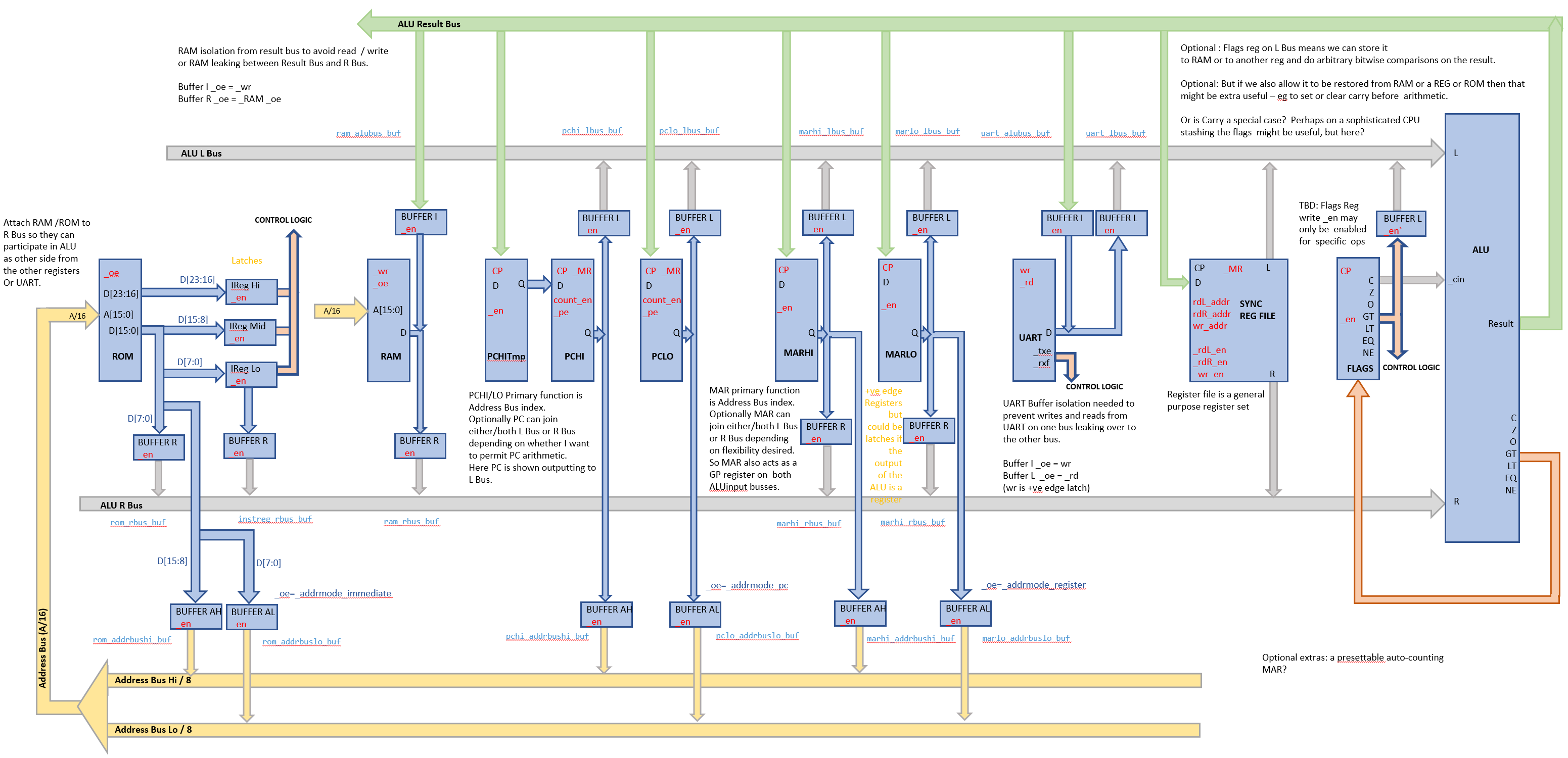
So the beastie I'm trying to implement is shown in the image below.
There's an 8 bit ALU which has "left" and "right" input buses for the arguments; everything goes via the ALU.
There are a bunch of devices, including the ROM, RAM, UART, memory address registers, PC and a small register file that can optionally output onto either the left or right ALU input bus. The output of the ALU feeds back into these devices.
I might not implement all these options in hardware. For instance in the design above the two MAR registers can act as general purpose registers due their participation as inputs to the ALU. However, I decide not to bother allowing the MAR to feed into the ALU on either or both channels. Also, likewise perhaps I won't bother allowing read access to the PC. Also, I show the flags register as potentially being an ALU input; also only an option. However, there's an initial core I will definitely build.
The register file is build using a pair of 74HC670's (4x4bit reg files). I wanted to find a place for these async chips out of curiosity, but the other registers like the MAR are regular 8 bit +ve edge registers. The async nature of the 74HC670's adds some complexity but since this is all an experiment and learning exercise I'm not too bothered about that and I've put a synchronous register on the data in to the register file to prevent feedback loops through the ALU.
But anyway, I've now got a simulated design now that lends itself to incremental extension, where I can get a simple functioning CPU together and then extend it gradually in various directions to ultimately end up with the full blown thing below if I have the stamina.
This looks like quite a challenge to me, and having written the control logic in verilog I know it's going to be a mess of wires.
The design effectively has 4 or 5 busses and given this is being built on bread board I'm probablyt going to use ribbon cable for the bus rather than use the power strips as I've seen other do.
I'm going to give it a try anyway - and find out if this effort leaves me any time with the family at all - or drives me insane.
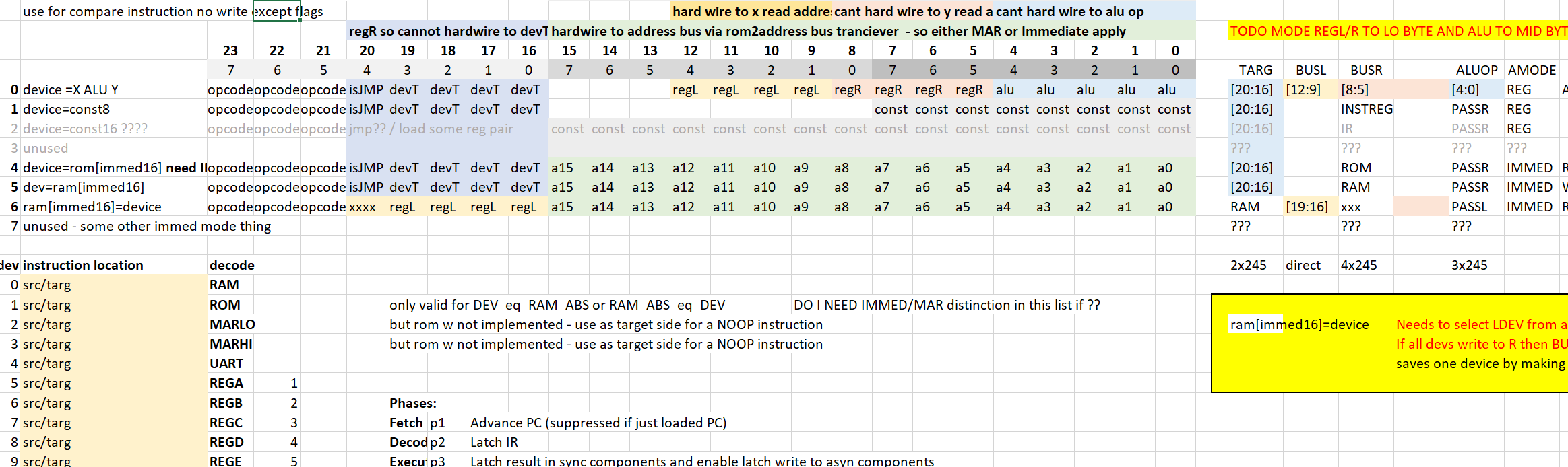
The instruction set is really designed around the idea that all ops really do is move data from one place to another and perhaps transform is along the way, and I've crammed these into 24 bits. I've just going to use three roms for this nothing too clever.
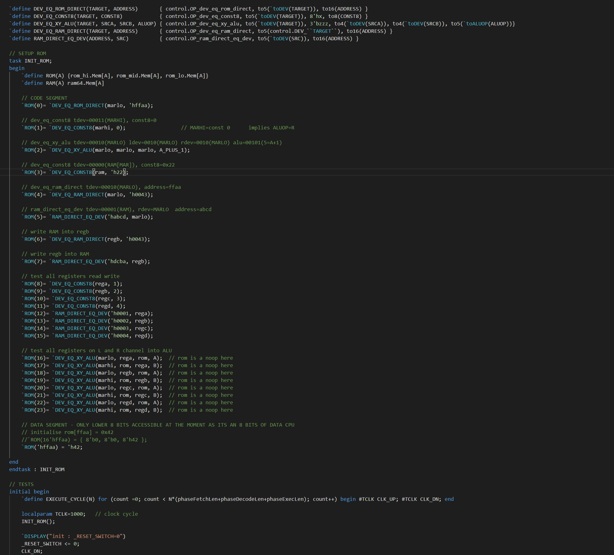
There are only 5 instructions and in the verilog I've created a kind of pseudo-assembler in the tests ...
So using these macros I can directly program the ROM in the verilog simulation with a bunch of tests cases rather than using a separate set of data files as the ROM images. There's a lot of benefits to this not least that it's a 100x easier to understand and develop, but also the fact I've used macros means my logging makes a lot more sense.
Along the way I've also come up with curiosities like an interactive Verilog UART implementationt that reasonably closely honours the UM245R behaviour. That was pretty interesting.
So tonight I plumbed in one of the last components, the register file. I've decided to use diode logic to the control lines into this component just for the experience. Not sure it will save any space but it may be interesting to use multuiple techniques.
I think the last two things I have to add are the flags register and the jump logic.
That will probably take a few more evenings.
Then I have to find a space in the house where my wife will let me make a huge mess of wires.
-
Interactive Verilog UM245R UART
04/21/2020 at 12:31 • 0 commentsWhat I need to make the verilog simulation of my (or any) CPU interesting is some I/O.
Many home brew CPU implementations include a UART of some kind. In my case I'm following the suggesiton of Warren Toomey (Crazy Small CPU) by using a UM245R.
I my other project the "Integrated Circuit Tester" I put together an interactive GUI and decided I wanted some interactive capability for my UART sim.
I've seen a couple of UART implementations in verilog but all I've seen is a static sim that is transmit only to the console with no receive function and no interactivity. I thought I'd see if I could advance this.
Scheme
The approach I've taken is to simulate the behaviour of the _RD/RW/_TXE/RXF interface of the UM245R and hook the implementation of the UART up to some bidirectional file IO.
Using this approach I can send interactive commands at the UART to tell it to receive or transmit bytes and I can also see any bytes "transmitted" by the UART. The interactive "client", if you want to call that, in this case is a couple of Linux 'cat' commands each talking to a file. One to file "/tmp/uart.control" to send instructions to the UART and the other file "/tmp/uart.out" to collect the transmit output of the UART.
The code is here https://github.com/portingle/spam-1/blob/master/verilog/uart/um245r.v
Commands
The currently supported instructions are...
- tXXX = Permit the UART to send a certain number of bytes where XXX represents the number. The _TXF line remains low until this number of bytes has been transmitted to the UART by the application code in the CPU by strobing the WR input.
- rSomeCharacters = Populate the receive buffer inside the UART with a collection of characters. Doing this drives _RXF low signalling to the application code in the CPU that the UART contains data to be received by the CPU. The CPU reads the data byte by byte by strobing _RD. And, _RXF returns high once the CPU has consumed all the data.
- /some comment = This appears on the console in the simulator.
- #interval = Instructs the UART simulation to allow time to advance by this many clock intervals. The UART uses a nanosec timebase. So '#10000' means execute a 10000ns verilog delay. See note below on timing.
- q = Instructs the UART to shut down the simulation. This is a call to verilog "$finish". I've found that If one is sending data to a verilog "$dumpfile" then that data isn't reliably available until the sim quits. So before visualising any timings I do a 'q'.
It's perhaps interesting to note that read of the control file currently the UART blocks the simulation. So time doesn't advance in the sim unless we send a comment to the UART to tell it to allow time to progress. This is the purpose of the '#' command. If we want the CPU to have an opportunity to consume or transmit data after a 't' or 'r' command then we need to tell the system to let time advance. I might also add a 'd' for 'detach' to let the sim freewheel.
Also, of note is that the file "/tmp/uart.control" can be used for replay purposes too if I want to rerun the same set of instructions.
Testing/Demoing
At the moment I have a test harness acting as the CPU around my UM245R component. The test harness is coded so that as soon as _RXF goes low it starts strobing _RD to read all the data, which it then dumps to the console. Likewise, if _TXE goes low then the test hardness is coded to start sending data by strobing _WR; at present it merely sends a sequential counter value to the UART (0 to 255 and wrap-around).
So, for example a command sequence might be/Starting test rHelloWorld #10000 /Ending test q
This sequence prints a comment in the sim console, puts "HelloWorld" into the UART receive buffer, tells the UART to let time advance by 10000ns, prints another comment to the console, then quits.
For a result like this from the test ...
VCD info: dumpfile dumpfile.vcd opened for output.
[      0ns] TEST: START
  50ns UART: reset end
[    150ns] opening uart.control
[    150ns] opening uart.out
[    150ns] fifos open
[    150ns] /Starting test
[    346ns] TEST: RECEIVED     Dec= 72 Bin=01001000 Hex=48 Char=H
[    632ns] TEST: RECEIVED     Dec=101 Bin=01100101 Hex=65 Char=e
[    918ns] TEST: RECEIVED     Dec=108 Bin=01101100 Hex=6c Char=l
[   1204ns] TEST: RECEIVED     Dec=108 Bin=01101100 Hex=6c Char=l
[   1490ns] TEST: RECEIVED     Dec=111 Bin=01101111 Hex=6f Char=o
[   1776ns] TEST: RECEIVED     Dec= 87 Bin=01010111 Hex=57 Char=W
[   2062ns] TEST: RECEIVED     Dec=111 Bin=01101111 Hex=6f Char=o
[   2348ns] TEST: RECEIVED     Dec=114 Bin=01110010 Hex=72 Char=r
[   2634ns] TEST: RECEIVED     Dec=108 Bin=01101100 Hex=6c Char=l
[   2920ns] TEST: RECEIVED     Dec=100 Bin=01100100 Hex=64 Char=d
[  10150ns] #10000 delay end
[  10150ns] /Ending test
[  10150ns] QUIT
(!) One thing to watch out for is NOT to take _RD and WR low at the same time. I don't know what the defined behaviour is for the hardware as I didn't get an proper answer from FTDI. In the case of RAM the write typically wins over a read so I was expecting something similar - but not documentedf.
SPAM-1 - 8 Bit CPU
8 Bit CPU in 7400 with full Verilog simulator and toolchain