-
A new project : Isetta
04/02/2023 at 08:32 • 0 commentsCheck my new project, the Isetta TTL computer ! It will be a single board TTL computer with video output, that can run 6502 programs and also Z80 programs at a good speed ! It is expected to run Apple ][, ZX Spectrum and Commodore 64 programs with only minor changes. The sprites in the Commodore will be a real brain breaker, and although the microcode will will be able to transfer one pixel per cycle to the video RAM (in a small unrolled loop), it is unsure if that will succeed.
-
C compiler, Assembler, Simulator source code
08/18/2020 at 15:25 • 0 commentsToday 20200818 I uploaded the source code of the software to the files section. All files should be placed on a webserver.
Compiler.php is programmed in PHP and has two big sections:
- Convert C source code to syntax tree (in an array-based format, described in the same file).
- Convert the syntax tree to an Abstract Syntax Tree (AST) with standardized JSON format.
Generator.js is programmed in Javascript, and also has two big sections:
- Analyze the AST and do several optimizations.
- Generate assembly code for the Kobold K2 CPU. The generator also does optimizations and can call the analyzer to assist in optimizing.
Simas_k2.js is programmed in Javascript, and has also two big sections:
- The assembly code (in most cases coming from the generator) is assembled, resulting in machine code.
- The CPU can be simulated. The machine code can also be downloaded to the K2 CPU.
Index.php is programmed mainly in HTML. It provides the IDE display and edit functions and calls the previous sections if needed.
Also included are a demo function, and a few manuals that can be activated in the IDE.
-
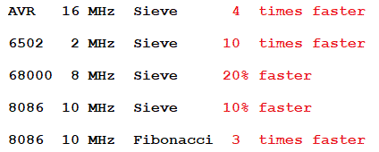
How fast is this thing, anyway ?
07/18/2020 at 15:47 • 2 commentsIt is interesting to know how the performance of the Kobold K2 compares to well-known processors. I did compare it to:
- AVR (16 MHz)
- 6502 (2 MHz)
- 68000 (8 MHz)
- 8086 (10MHz)
Summary
If you don't have the time to read the whole log, here are the results for a Kobold at 6.25 MHz:
![]()
Kobold processor running the Sieve program
There is only one classic test that is familiar, very often used, and easy to perform:
It's called the Sieve of Eratosthenes.
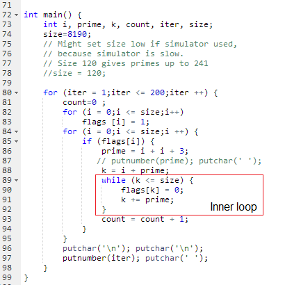
Here is the C source code for Kobold K2:
![]()
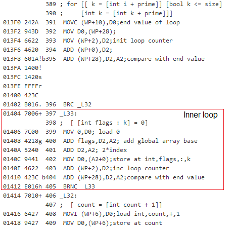
The Kobold C compiler generates the following assembly code:
![]()
For the speed, the inner loop is the most important. You can see here that the loop has 7 instructions, that is 14 cycles (every instruction takes 2 cycles).
The prototype runs from a 25 MHz oscillator, and the cycle speed is 1/4 of that: It does 6.250.000 cycles per second.
The whole sieve program (10 iterations) took 3.3 seconds (timed with an app on my phone).
Compare with AVR
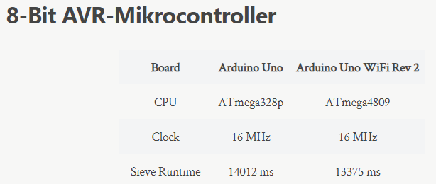
I found in this article that the 16 MHz 8-bit AVR takes 14 sec to do the benchmark:
![]()
So for the sieve, 6.25 MHz Kobold K2 is around 4 times faster than a 16 MHz AVR !
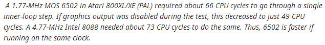
Compare with 6502
In this post someone describes the performance of his hand-optimized assembler sieve code for the 6502, taking 49 cycles for the inner loop:
![]()
In our case, Kobold K2 does in 14 cycles what the 6502 does in 49 cycles. That makes Kobold 3.5 times faster.
But Kobold's cycles are faster: 160 nS. For a 2 MHz 6502, cycles are 500nS. So this gives another gain of 3.125 in speed.
So for the sieve, 6.25 MHz Kobold K2 is 10.9 times faster than a 2 MHz 6502 !
And it does not even need hand-optimized assembler code to do this. The C compiler does its job well !
Compare with 68000
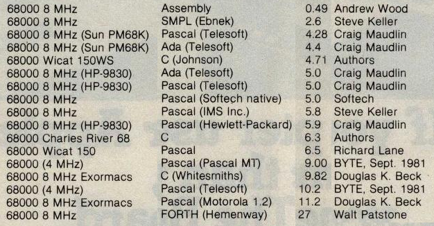
In a follow-up article, Byte jan 1983, many users shared their result for the sieve running on an 8 MHz 68000, compiled by several compilers:
![]()
The highest speed was 0.49 sec for an assembly program, and the lowest 27 sec for a Forth system.
To our surprise we see that in this test, the 6.25 MHz Kobold K2, with its 3.3 seconds time, beats all C, Ada and Pascal compilers targeting an 8 MHz 68000 !
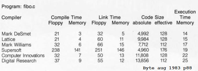
Compare with 8086
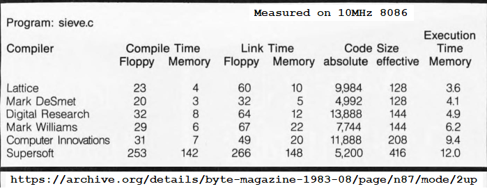
We use this Byte article from aug 1983 for comparing with the 8086. The benchmarks were performed on a 10 MHz 8086.
![]()
In the sieve test, the 6.25 MHz Kobold K2, with its 3.3 seconds time, beats all C compilers targeting a 10 MHz 8086 ! The Lattice compiler comes closest with 3.6 seconds.
Compare speed of function calls
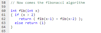
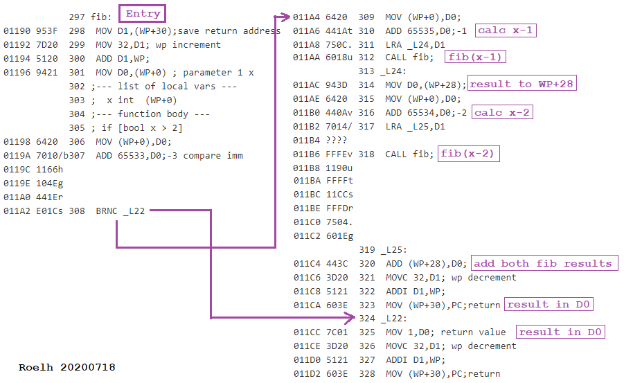
The sieve program test mostly loop and array performance. In the mentioned 1983 Byte article , there is another interesting test. It is calculating Fibonacci numbers with a recursive algorithm. It is very inefficient, but it does a lot of function calls, so it is very suitable to measure the efficiency of function calls and returns.
![]()
The following is the assembly listing after C compiler and assembler did their work:
![]()
This function is called with the value 24 as argument, that's the highest number that gives a result still fitting in 16 bits. Just as with the sieve, the fib(24) call is repeated 10 times, and the total amount of time is recorded.
On the Kobold K2, this took around 5 seconds.
Let's see what was reported for the 8086 back in 1983:
![]()
The result is even better than with the sieve program:
In the fibonacci test, the 6.25 MHz Kobold K2, with its 5 seconds time, beats all C compilers targeting a 10 MHz 8086 with a factor 3 or more !
-
Never too late to change the instruction set
06/27/2020 at 20:31 • 0 commentsDuring work on the C compiler it appeared that the instruction set had some problems. Compiling was possible, but sometimes resulted in code that was longer than optimal. (Of course the lack of AND, OR and XOR also can give longer code, but that was accepted from the beginning and I won't change that. Not now :) ).
The main problems were:
- When storing a register to memory, the contents of that register changes
- Move from one data register to another one is not possible.
- Instructions with 3 operands exist, but placed strong restrictions on the involved registers
- Compare instructions don't exist. An ADD is used instead, with unwanted effect that the sum is written to a register.
Of course the change must be small, because I will also have to change the hardware prototype and I don't want a lot of rewiring.
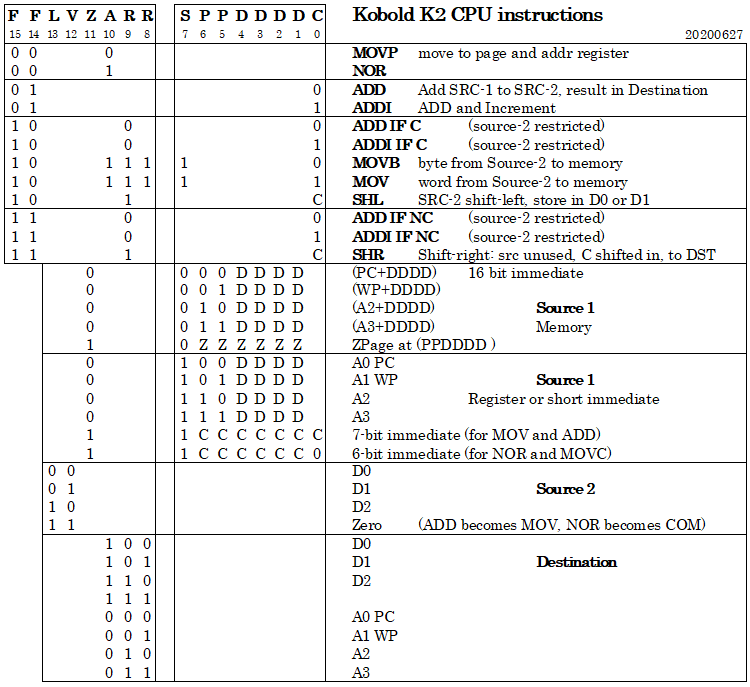
CHANGES
The main change is the introduction of many 3-operand instructions. The second operand is always a register, and when this is register D3, this transforms a ADD in a MOV because D3 is now always zero. A new RISK feature !
The other problems were also addressed. Of course new restrictions appear: Register D3 can not be used to store a value. The number of Z-page addresses goes from 128 to 64, and the result of a shift instruction always goes to D2.
The new features:
- When storing a register to memory, the contents of the register stays the same.
- All register-to-register moves are possible.
- Many 3-operand instructions available.
- A CMP instruction is introduced (it is an ADD instruction, but only writes CY and doesn't change a register.
Some other new instructions, that were not in the problem list but are quite useful:
- A memory position can be cleared without having to load a register with zero (The CLR instruction stores the always-zero D3)
- Many register-to-register instructions can be conditional (executed when CY is 0 or 1).
- Many MOV and ADD instructions (also 3-operand versions) can be conditional
The new set needs one extra AND gate. That's an extra IC. Perhaps a few of the other gates can also get a useful function....
SO HERE IT IS
![]()
TODO
- change the assembler
- change the manual of the assembler
- change the simulator
- change the C compiler
- change the hardware
[ add 2 weeks of changes and debugging ]
DISILLUSIONMENT
After more than two weeks, I could not get this to work. Many opcodes changed, requiring changes at several places. The automatic jump-size detection and associated complexities did not do what I wanted them to do: the programs would not run well on the simulator, so I didn't even dare to change the hardware and test on that.
So I gave up on that.
Then came a few days that I worked on a simpler form of these changes. I got the assembler and simulator working, but after modifying the hardware I got non-logical behaviour of initialized global variables. Difficult to debug. Or build a debugging tool first ?
Yesterday I decided that it was not worth the trouble. I rolled back all changes from this log.
Except one change: there will now only be 64 zpage variables (instead of 128). Like 64K, 64 globals should be enough for everybody. This leaves us one bit (Instruction bit 7) totally free for later use. So, only 50% of the instruction space is used !
-
Running C at full speed
06/02/2020 at 13:26 • 2 commentsIt's been a while since the last log. I could not spend much time on the project lately.
Progress was made on the C compiler. It now handles initializers, strings and chars, all needed for the "Hello World" program. On the hardware side, U41 was placed, that is needed for reading chars from the upper half of a word.
Finally I was now able to get a real C program running on the hardware !
On the hardware I mounted the 25 MHz oscillator, and selected it by mounting R2 and removing R5 (that connected to the 460 kHz RC oscillator). The timing loops for the synchronous character transfers were now 750 instead of 15, to account for the 50 times higher clock frequency.
The combined Hello-World and prime number program were also running at the intended speed, 25/4 = 6.25 MHz cpu clock, that is 3.125 million instructions per second (one instruction is a fetch cycle and an execute cycle).
The simulator runs quite slow, and would be practically useless with two 750 cycle loops after writing a character. The simulator already checks for a write to 0xF000. After writing a character, the simulator has extra code that will directly return from the putchar function, bypassing the loops. Now a single program will run on the simulator as well as on the real hardware.
So what is next ?
- start designing the video display unit
- arrange a keyboard for the Kobold
- have a small operating system, that itself is programmed in C (suggestion anyone ?)
-
Introducing the C compiler
03/13/2020 at 21:00 • 0 commentsThe Kobold K2 processor is quite suitable to run a language like C.
Fortunately I had started a compiler project several years ago, but I never finished it. So now I had the opportunity to get some results from all the hours that already went into that project.
Another possibility would be to use an existing compiler and change the code generation part. Several C compilers generate pseudo-instructions, that only have to be translated to instructions for your own CPU. But since the Kobold is such an odd beast, it is needed to have control over the code generation at a high level, to get an acceptable code output. And I had the unfinished project as a start point, so that was the way to go.
My compiler project started in the period that I discovered that you could program a HTML server to generate webpages using the PHP language, and that PHP was actually a full featured programming language. To make a long story short, the compiler was programmed in PHP and ran on the webserver.
It generated some intermediate code. Many of my fellow HAD'ers could face a similar simulation (wanting to generate code for your homebuilt processor, but having difficulty in interfacing to an existing front-end compiler). How much easier would it be, if the intermediate code was standardized ?
I here propose a standard interface between the parser and code generator. If this interface is standardized, a codegenerator for a certain CPU can be used with all C compilers that comply to this standard. It is described HERE (but is not fully complete yet). Its syntax is JSON.
In the last months, I added (to my PHP compiler) a section that translated the old intermediate code to the new JSON standard. I then started with the code generation section, programmed in Javascript. The code generator does several optimizations. The resulting assembly code is reasonable compact, and also fast because native code is generated. Finally, the K2 assembler produces the binary code.
The C compiler is now integrated into the Kobold K2 online Javascript assembler/simulator. The generated assembler code is displayed side-by-side to the C source code. The C code can be written in the included online editor that has syntax highlighting, matching parenthesis indication and several other features (it is the ACE editor that was integrated here). The C compiler is not yet full-featured. Its capabilities are in the Language Manual (also reachable from within the online editor)
On a single browser page you can now edit, compile, assemble and simulate the C code, and download a file to flash it into the Kobold. With the 'assembler' checkbox, it is still possible to program directly in assembler.
See it live at http://www.enscope.nl/simas_kobold2/ !
The page loads a prime-number generator as demo program. You only have to press the RUN button to start it. However, the simulator is quite slow because it simulates almost at the gate level (see comments in the C code of the demo).On the hardware side, the bug in the NOR instruction was found (a short on the pcb), and the RAM is now also working.
-
Milestone: Hello world !
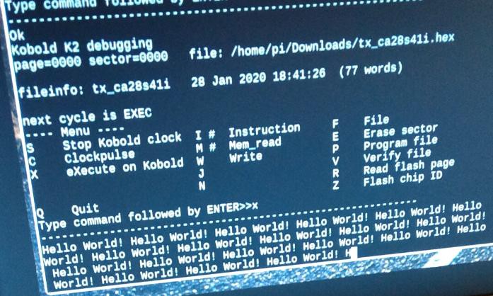
01/28/2020 at 19:40 • 2 commentsA milestone for every CPU project: print "Hello World !" !
![]()
SERIAL PROTOCOL
Having text output could have been a project all on it's own... but here I use the Raspberry Pi as terminal. On the main board of the Kobold, the connector to the RPi has two pins that are used here:
- signal SPI_CS3/ pin 11, RPi GPIO 11, clock signal coming from Kobold
- signal SPI_MOSI / RPI_DATA pin 2, RPi GPIO 13, bidirectional data
A simple synchronous protocol is used. The Kobold sends a clock signal, and on the data line it puts the character, complete with a startbit (low) and a few stopbits (high). It is intended that the RPi will be able to send data back over the same line, using the other edge of the clock signal. So the RPi can be the terminal for Rx and Tx, as long as there is no other way to do this.
The Python script at the RPi side got an extra section, started with the 'X' command, to receive the characters and put them on screen.
FILENAMES
A remark about the filename, you see on the screenshot that the TX program is named tx_ca28s41i. The reason is, that when you download the file from the webpage, you will get 3 files:
- TXT file with source code
- HEX file to put in the Flash
- LST file that shows the assembled source code
During debugging, you will download a lot of times. By always downloading the source at the same time, with the same timestamp (ca28s41i), you can always trace the source that belongs to an executable. And when replacing the binary file in the Python script, you only have to type the four last characters (thats the time-of-day) to replace the binary file with a newer one.
HELLO WORLD PROGRAM
And here is the program, dominated by the section for serial transmit:
; Kobold K2
; program name: TX
; character TX to RPi
; 20200128

start:
 nop
 movp 0,wp ; set wp page to zero
 movp 0x20,a2 ; A2 output address:
;
; A2+16 spi_cs3 low (char clk)
; A2+18 spi_cs3 high (char clk)
; A2+24 MOSI low
; A2+26 MOSI high
;
; A2+28 led on
; A2+30 led off

reset:
 mov data,A3
 jmp there

loop:
 mov D3,A3 ; restore A3
 add 2,A3  ; every char is in a word !
 mov (A3),D3
 add 0xffff,D3 ; test for zero
 brnc reset


there:
 mov (A3),D0
 mov A3,D3 ; save A3 in D3

;-- function for char transmit --
; input char in D0
; return address N/A
; I/O register addr in A2
; first comes a startbit (low)
; then data, highest bit comes first
; then comes stopbit (high)
tx:
 mov 0xfff4,A3 ; bit counter
 shl D0
 shl D0
 shl D0
 shl D0
 shl D0
 shl D0
 shl D0 ; now shifted 7 times
 ; put start and stopbits
 add 0x007F,D0 ; stopbits high. startbit already ok.

; set data line high or low depending
;     on bit shifted out of registerD0
bitloop:
 mov D2,(A2+24) ; data low
 shl D0
 brnc bitlow
 mov D2,(A2+26) ; data high
bitlow:

; delay section
 movc 6,D2 ; bit timer
bitdly1:
 add 4,D2
 brnc bitdly1
 mov D2,(A2+18) ; clk high

; delay section
 movc 6,D2 ; bit timer
bitdly2:
 add 4,D2
 brnc bitdly2
 mov D2,(A2+16) ; clk low
; count number of bits to transmit
 add 1,A3
 brnc bitloop

; small delay after character
 mov 0,D2 ; bit timer
dly1:
 add 20,D2
 brnc dly1

; mov D0,PC ; ret

 jmp loop  ; do next character

 data section

data:
; dw newline
 dw 'H'
 dw 'e'
 dw 'l'
 dw 'l'
 dw 'o'
 dw ' '
 dw 'W'
 dw 'o'
 dw 'r'
 dw 'l'
 dw 'd'
 dw '!'
 dw ' '
 dw 0
I had to avoid the NOR instruction, that has an error in one of the 16 result bits. I expect that won't be difficult to trace.
There is still no RAM mounted. All the data required for the "Hello World" program could be kept in registers.
-
Blinking LED !
01/25/2020 at 19:37 • 0 commentsA major milestone reached today.
The Kobold K2, without debugger attached, runs a program from its two Flash ROM's, and blinks the LED on the main pcb !
It runs on the RC-clock that is on the main PCB (U9A, HC132, 4K7 and 470pF). No RAM has been mounted yet.
Here is the program:
; Kobold K2
; Blinking LED
; 20200125

start:
 nop
 movp 0,WP ; set wp and its page to zero
 movp 0x20,A2 ; address and page of output register

loop:

delay1:
 add 4,D0
 brnc delay1

 mov D1,(A2+28) ; led on

delay2:
 add 4,D0
 brnc delay2
 mov D1,(A2+30) ; led off
 jmp loop
Some notes about the program:
- The output is an addressable latch. Address bit A1 tells if the LED is on or off. So the value that is written to the address is unused, so there is no initializing of the D1 register needed. After a reset, this latch is reset and the LED is ON. So the LED is also a power indicator.
- The loop counter in D0 is never initialized. After adding 4 enough times, there will be a carry and the delay loop ends. At that moment, D0 has a low value again and can be used for the next delay loop.
- The WP (workspace pointer) is not used in the program, but it must be initialized otherwise the 8-bit immediate modes won't work.
- MOVP 0x20,A2 will set A2 to 0x0020, and it's page will be set to the lowest 4 bits of the 0x20 value, so it's page is set to zero. (Similar for WP that is set to zero).
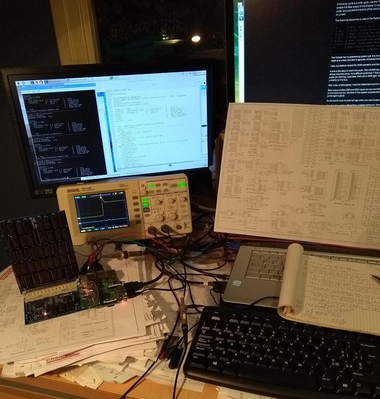
It took about two weeks to reach this point. And of course, a job and other obligations limit the time that is available for the project.
My desk during the debugging:
![]()
Just a summary of the things I encountered. This is mostly for myself, if I loose my notes then I can find here what I did. The notes start before the previous log, the numbers are the item numbers in my notebook.
1)
A problem with the clock generator on the main pcb. The Kobold needs two clock signals, on the main pcb these are called CPU_CLK/ and CLK2/. CPU_CLK/ must get active first, and stay active for 75% of the time. CLK2/ comes later, is active for 50%, and both clocks should end around the same moment. This phase relation was not correct. After the correction, CPU_CLK/ had a spike, that was removed with a small RC network. The final correction to the schematic was:
At pin 2 of U10A, a low-pass network 470E 33pF was inserted. U7B pin 11 was disconnected and connected to U7A pin 5.
3)
On the main board, one of the holes for the power connector was not big enough.
6)
Created S, I, M commands in the RPi script for debugging, see previous log.
7)
During debugging, the clock coming from GPIO8 is inverted wrt the CPU clock. This is not a problem, but if you don't know this, you get strange results.
8)
The HC299 did not put its contents on the bus (see previous log). Disconnected pin 1 and connected it to its pin 2 (on both devices). The shift-left function of the HC299 is now no longer available, but is now done by storing the register at any position in memory. This has as side-effect that the ALU adds the data register to itself and stores the result in the same register. And, surprisingly, the opcode doesn't even change. [edit: just found out the hard way, that the opcode does change. It is now the same as for a store instruction]
10)
Resistor R2 should get a more logical position on the pcb. Due to its strange position, I forgot to solder it.
12)
Started working on the Flash programmer. Starting point was the RPi Python script for the Risc Relay CPU. The RRC can only address words, while in the Kobold address bit A0 selects low or high byte, and is not connected to the Flash address bus. So the addresses had to shifted. Note that the RPi uses Kobold instructions to let the Kobold provide the correct address to the Flash. Both 8 bit Flash devices are programmed in parallel as if it were a single 16 bit wide device. The RPI provides the WE/ signal (on GPIO 25) to the flash to program it.
13)
The CE pulse from the RPI (Called DATA_EN/ on the main board) doesn't reach the Flash. It seems this can only reach the flash while the Kobold clock is active. (CE is needed to read from flash). First thing to check, before programmming, if the manufacturer and device ID can be read from the flash.
14)
Programming was working, but very unreliable. Problem was the 5V - 3V3 conversion. The connection board to the RPi has resistor dividers that bring 5V signals from Kobold down to 3V3 for the RPi. In the other direction, the 5V chips 'should' just accept 3V3 as high. In my previous projects, I used 5V powered HCT chips at those positions. Here I use HC and AC chips, and apparently did not think much about it.
In the end, I lowered voltage to the Kobold to 3V3. Both HC and AC can work at that voltage, and even programming the 5V Flash worked at 3V3. A final solution would be, to have a both-way voltage conversion to the RPi. To be done later.
15)
Problem with step-by-step executing from flash. It seems that the incremented PC is not written well to the HC760. Check if WE/ (U36 pin10) goes high before SHFT_OE/ (U26 pin 1,2,3) goes high. The difference is difficult to measure, seems to be less than 3 nS. This was anticipated as possible problem. C50 was not mounted yet, now mounted 120pF that gave about 10nS margin, looks enough.
Also, a problem was found with the reset. But this can be solved later, because for now, the CPU can be reset by giving commands from the RPI (instructions to reset PC and its page to zero).
16)
Now I had a strange problem, when executing commands from the debugger. Sometimes, bit 5 got set in the data. After trying several combinations, I got it reproducable. It occured when the WP and its page were initialized to zero. The instruction is "MOVP 0,WP" and it is assembled as opcode 211E. This is 16-bit immediate mode. It assumes the programcounter points at the beginning of a 32-byte chunk, and the LSB of the instruction tells that the immediate value can be found at PC+0x1E (the last address of the chunk).
When entering the instructions from the debugger, just enter "I 211E" and then the operand "M 0000". Never mind the value of the PC. The Kobold won't mind that the operand doesn't come from memory.... BUT... The programcounter does have a certain value, and when the 0x1E is added by the adder chip U32, there will be a carry when the PC is not zero... This carry goes to the OR chip U42C to bit 5 of the adder chip U6 of the ALU... causing 0x20 to be added to the data ! That is the way it is designed. It is used for adding a small constant to an address register. When the small adder U32 overflows, the carry is handled by the main ALU.
So when you don't know the PC value during debugging, use "2100" for loading the WP, that will add 0 in the U32 adder and will never generate a carry there.
If you have a strange architecture, beware that you will have strange results during debugging...
Another one in the same category: Some instructions contain an 8-bit immediate operand directly in the instruction. Moving the value 0x34 to register D0 has code "7C34". So we enter the instruction with the I command, and for the execute cycle we just enter "M 0", knowing that this data is not used, because the processor already has the 0x34 value. Wrong. It just loads zero instead of the expected 0x34.
The "M"command disables outputs from Kobold or Memory, so the RPi can put that value on the bus. But in Immediate 8-bit mode, the Kobold first places the immediate data on the databus with the buffer unit, and then the ALU reads that data as if it was coming from memory ! The M command disables the buffer unit, so the "M 0" zero is going to the ALU ! So use the W command instead, that generates an execute-clock-pulse but lets the Kobold or memory drive the databus.
18)
The problem with the reset, mentioned earlier, is solved with a hardware modification. The reset connects to the instruction register (setting it to zero) and to the shift unit (setting it to zero). So at reset, it will execute an instruction with opcode "0000", that will write a value to the PC and to the page of the PC. Resetting the shift unit makes that the written value is zero. BUT... we have no control over the moment that the reset pulse ends. When it ends, the shift unit will at the following clock be filled with some value from the ALU, while the instruction register still has the instruction to send that value to the PC. So, a probably non-zero value, coming from the ALU, will be put in the PC.
It was solved by driving the reset of the shift unit also from the instruction register, by decoding sufficient bits of the "0000" instruction:
Decoder U44B is now used (was unused). Its input pin 15 connects to pin 4 of U44A, and its input pin 14 connects to pin 15 of U43. Its output at pin 12 now connects to the CLR inputs of U25 and U26 (pins 9).
999)
Well that was a not-too-short list of challenges that I encountered before I got the LEDs blinking.
Now I have a Blinking LED..... yes I could also do that with a 555...
-
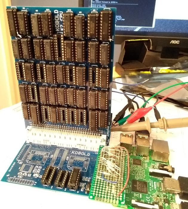
Datapath working !
01/03/2020 at 16:17 • 4 commentsToday I got the datapath working ! I mounted all parts, except those that are in the address generation section, because I wanted to start small. Also, no memory is mounted yet.
![]()
As intended, the main board connects to a Raspberry Pi. At this moment, the connection has:
- 16 databus lines
- clock_enable ENA output to Kobold (GPIO24, low to disable Kobold clock)
- clockpulse CLK output to Kobold (GPIO8, clockpulse is active high)
- chip-enable CE output to Kobold (GPIO3. If high, Kobold and memory will not drive the databus)
- EXEC signal from Kobold to RPi. Low for an exec cycle, high for a fetch cycle.
The RPi can control the Kobold, that is needed for debugging and lateron for programming the flash. It will use the ENA output to stop the clock of the Kobold. It can then use the CLK to give a single clockpulse, and watch the EXEC signal to see if Kobold expects a Fetch or Exec cycle.
In a fetch cycle, RPI must make CE high, then put an instruction on the databus, and give a clock pulse. The Kobold will place the instruction in the instruction register (U27 and U28) (with the "I" command in the Python script). The following exec cycle can be a read or write cycle. In a read cycle, the script must put data on the databus ("M" command in script) and give a clock pulse. The Kobold will think that it reads this from memory.
If the exec cycle is a write cycle, use the "W" command in the script. The RPi must make CE low, to enable the data output of the Kobold. It must also make its 16 datalines input. It can now give a clock pulse, and just before the end of the clock pulse it can read the data on its 16 datalines, and put that on screen.
The following sequence is used in the Python script to add 1234 to 4321 :
S       # stop Kobold clock
I 6400  # fetch: instruction to load a word in register D0
M 1234  # exec: provide the data that Kobold reads from memory
I 4400  # fetch: instruction to add a word to register D0
M 4321  # exec: provide the data
I 9400  # fetch: write data from register D0 to memory
W       # exec: Kobold writes result to memory, RPi catches
                 it and displays 5555
The Kobold has no addressing system yet. It is not needed for this test because the RPi handles all reads and writes, and also is agnostic of Kobold memory addresses at this moment.
I also successfully tested the NOR operation and the data registers.
It took a few days to reach this point. The HC299 has kept me busy. You could write data in it, but it always returned zeros. How difficult could it be ? Two inputs determine what happens at a clock pulse: Do Nothing, Load data, Shift Left or Shift right. Two enable inputs must both be low to put the contents on the bus.
After a day of debugging, I read the datasheet word by word. And there is was:
Both output enable (OE1 and OE2) inputs are low and S0
or S1 or both are low, the data in the register is presented
at the eight outputs.So S0 and S1 must not both be high when you want output ! Always read your datasheets.
After that, the system suffered from unstable behaviour. Sometimes it worked, and the next minute it didn't. This was finally traced down to my start-small strategy, where the address generation chips were not yet placed. I simply overlooked that a control signal that was needed for the data system, was routed through one of the missing chips. The signal was now undriven, that explains the strange behaviour.
-
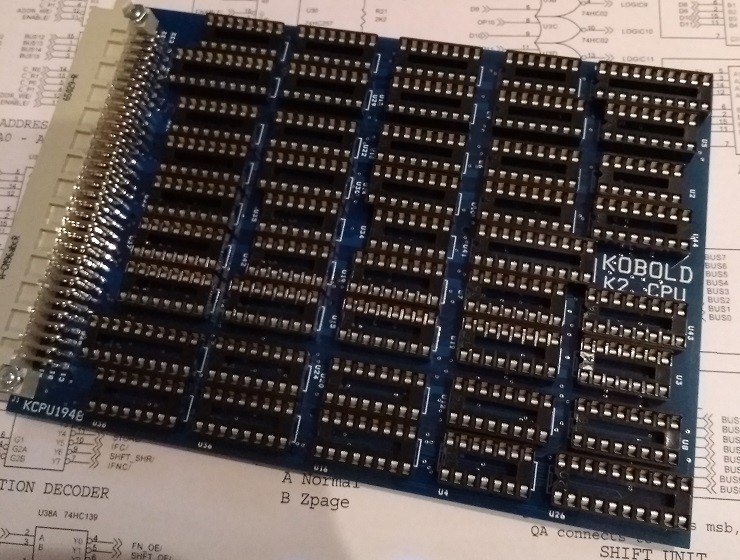
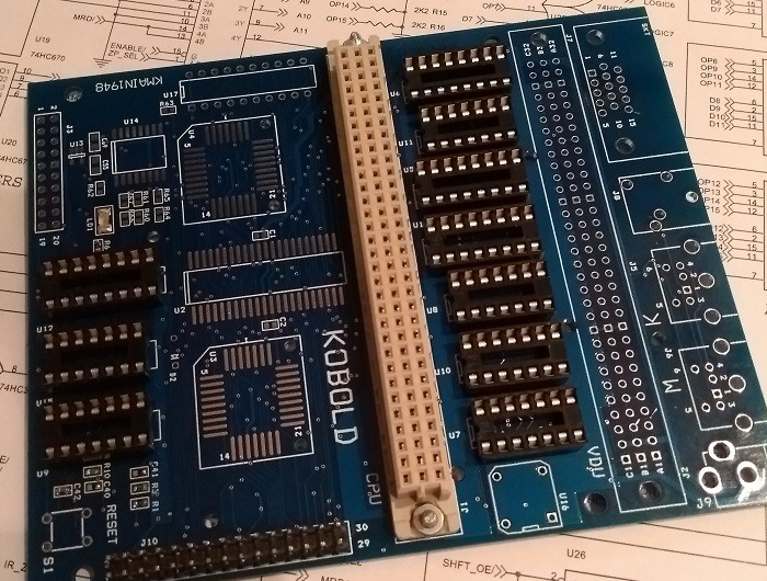
Started soldering
12/29/2019 at 22:00 • 0 commentsI started soldering the two boards. Here are the CPU and Mainboard, with sockets:
![]()
![]()
Kobold K2 - RISC TTL Computer
A 16 bit RISC computer with video display, from just a few TTL and memory chips. Online C compiler and simulator available.