land-boards.com
-
PIO Modes Working
10/31/2019 at 23:03 • 0 commentsPut in a level of support for the PIO.
It's not possible to completely emulate the PIO using an MCP23017 I2C Port Expander. The PIO has hardware handshake which runs automatically in particular modes. There's no support in the MCP23017 for hardware handshake. Plus the MCP23017 is much slower.
But emulating the PIO does work at some level. There are two 8-bit ports and they can be set to the same modes as the PIO:
- All inputs
- All outputs
- Selected pins in/out
The interrupt controller function needs work. The MCP23017 has an interrupt line which can be set when there is a change of an input pin. The PSoC can communicate with the MCP23017 to determine the interrupt source.
But, I'm happy with the operation as it is. I hooked an LED up to a pin, made it an output and then toggled the line from OUT commands in BASIC. Here's the BASIC program.
10 REM BLINK THE EXPANSION MCP23017 LED ON GPB7
20 REM SET PORT B INTO OUTPUT MODE
30 OUT 35,15
40 OUT 33,0
50 FOR I=1 TO 1000
60 NEXT I
70 OUT 33,255
80 FOR I=1 TO 1000
90 NEXT I
100 GOTO 40
-
DAC on the Z80_PSoC
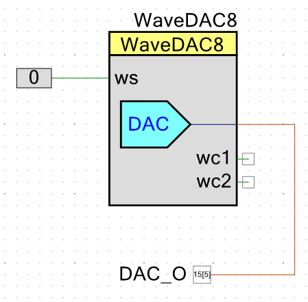
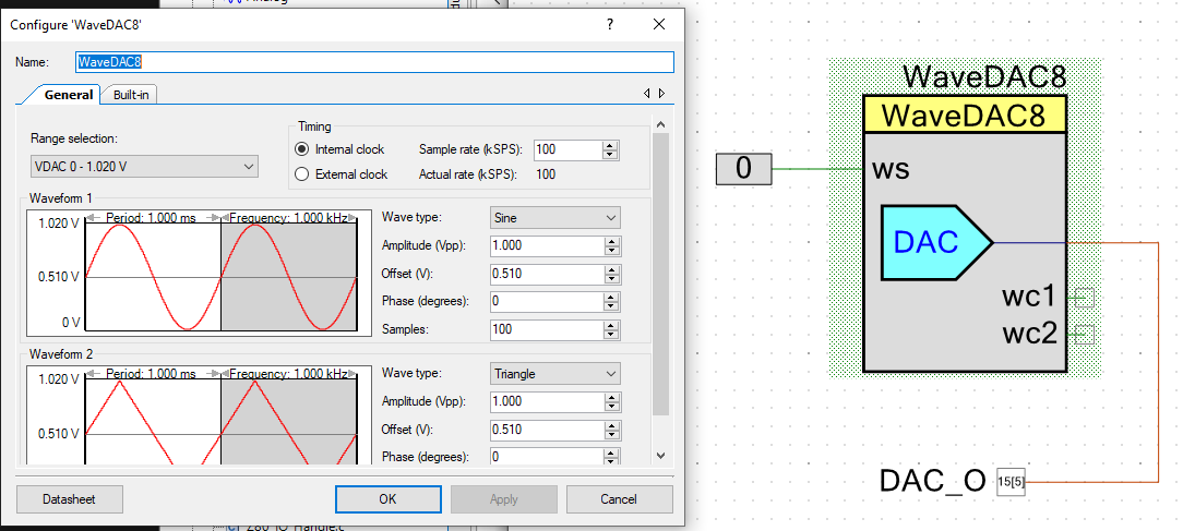
10/27/2019 at 11:30 • 0 commentsGoing to play with the DAC on the Z80 PSoC. Dropped the WaveDAC8 symbol on the schematic.
PSoC Pinout
Hooked up to PSoC pin 95.
Added code:
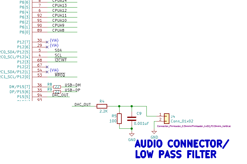
void init_DAC(void)
{
    WaveDAC8_Start();
}
Looked at R4 and saw sine wave.
Here's the DAC handler.
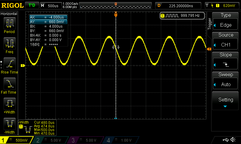
uint8 dacState;
uint8 outDataDAC;
uint8 inDataDAC;

///////////////////////////////////////////////////////////////////////////////
// void init_DAC(void) - Initialize the DAC

void init_DAC(void)
{
    WaveDAC8_Start();
    outDataDAC = 0;
    inDataDAC = 0;
}

///////////////////////////////////////////////////////////////////////////////
// void writeDAC(void) - Write to the DAC data

void writeDAC(void)
{
    outDataDAC = Z80_Data_Out_Read();
}

///////////////////////////////////////////////////////////////////////////////
// void readDAC(void) - Read the DAC data

void readDAC(void)
{
    Z80_Data_In_Write(outDataDAC);
    ackIO();
}

///////////////////////////////////////////////////////////////////////////////
// void readStatDAC(void) - Read the DAC Status

void readStatDAC(void)
{
    Z80_Data_In_Write(dacState);
    ackIO();
}

///////////////////////////////////////////////////////////////////////////////
// void writeCmdDAC(void) - Write the DAC command
//  0 = Turn off DAC output
//  1 = Turn on DAC output

void writeCmdDAC(void)
{
    dacState = Z80_Data_Out_Read();
    if (dacState == 0)
    {
        WaveDAC8_Stop();
    }
    else if (dacState == 1)
    {
        WaveDAC8_Start();
    }
    ackIO();
}
Here's the output,
1 KHz. Matches the setup in PSOC Creator.
-
SD Card Block Writes from the PSoC monitor
10/26/2019 at 18:40 • 0 commentsExample Code Out There?
Unfortunately, the code example that I used to develop the read block routine doesn't have a write block example so I don't have that as reference code to compare with my code.
I used the same code for the write that I have for the read and changed the CMD to the proper code for single block writes. I did leave in the same two dummy writes at the end but I wonder if there's some difference that I did not account for there? I see the two dummy writes for the CRC after the transfer in the SdCard.cpp file that is used for the Arduino. After the dummy bytes they pull the SD card status. They do that with a send of 0xff and read the result. I wonder if I need to do that with this card?
The SD card spec for SPI has:
"...every data block sent to the card during write operations will be responded with a data response token"
I tried an extra read at the end and got 0xFF. Can't tell if it's from the SD card.
Checking the Sector Number
The sector number I want to write to is 1GB / 512-bytes. The sector number for the block at the 1GB location is 0x20,0000,
To run the monitor I press the EXFP button on the Front Panel. If I didn't have the front panel I could just jump into the monitor but this way is flexible. Adding a function to write to the SD card when "W" is entered is relatively easy since I already have the command interface works.
Tried it and the reads don't match the writes. I don't know what's in the upper card contents. Is there a problem with having block numbers so high? The sector number is an unsigned long (32-bits) so the value 0x200000 fits. This translates into:
// S 0000 0000 0000 0010 0000 0000 0000 0000 - Sector Number // AD 0000 0100 0000 0000 0000 0000 0000 0000 - Sector shifted left by 9 // UP 0000 0100 - Upper byte // - >> 24 bits + << 9 bits = >> 15 bits // UM 0000 0000 - Upper middle byte // - >> 16 bits + << 9 bits = >> 7 bits // LM 0000 0000 - Lower middle byte // - >> 8 bits + << 9 bits = << 1 bit // LO 0000 0000 - Bottom byte- S is the Sector Number
- AD is the absolute address (S shifted left by 9-bits - 512-bytes)
- UP is the upper byte that is written out to the SD card
- UM is the next byte (upper middle)
- LM is the next byte (lower middle)
- LO is the lower byte (always 0's)
This actually does make sense. The address sent to the SD card is the absolute address where the bottom 9 bits are 0x's to match the 512 byte sectors. The bottom bits of the sector count get shifted left by 9 bits Since it's being written into the second address byte from the bottom it only gets shifted up by 1 bit.
LBA mapping to the Disk
This probably doesn't matter for this, but Grant's docs has:
![]()
Write Code
The write code looks like:
void SD_WriteSector(uint32 sector, uint8 * buffPtr)
{
    uint16 loopCount = 0;
    uint8 junk;
    SPI_write_byte(CMD24);            // CMD24
    SPI_write_byte(sector>>15);       // >>24 + <<9 = >> 15
    SPI_write_byte(sector>>7);        // >>16 + <<9 = >> 7
    SPI_write_byte(sector<<1);        // >>8 + <<9 = << 1
    SPI_write_byte(0);
    SPI_write_byte(0xFF);
    while((SPI_Master_ReadTxStatus() & SPI_Master_STS_TX_FIFO_EMPTY) != SPI_Master_STS_TX_FIFO_EMPTY);
The top byte of the sector number is in d15..d22. The read is attempting to happen with:
readSDCard(0x200000);
One problem was that I bumped up the SPI bus speed to 400 KHz but had the sample rate at 500 KHz so there was possibly some data dropped. After changing the sample rate to 500 KH this is what I see for the write:
So, I can see the writes and I know reads work when I read sector 0 because I see the CP/M code.
Read from the SD Card
0000  c3 5c d3 c3 58 d3 7f 00 43 6f 70 79 72 69 67 68  .\..X...Copyrigh
0010  74 20 31 39 37 39 20 28 63 29 20 62 79 20 44 69  t.1979.(c).by.Di
0020  67 69 74 61 6c 20 52 65 73 65 61 72 63 68 20 20  gital.Research..
0030  20 20 20 20 00 00 00 00 00 00 00 00 00 00 00 00  ................
0040  00 00 00 00 00 00 00 00 00 00 00 00 00 00 00 00  ................
But my code does the write, then does a read and it gets back something other than the expected pattern (0xff, 0xfe, 0xfd...).
Write to the SD Card
0000  00 00 00 00 00 00 00 00 00 ff ff ff ff ff ff ff  ................
0010  ff ff ff ff ff ff ff ff ff ff ff ff ff ff ff ff  ................
0020  ff ff ff ff ff ff ff ff ff ff ff ff ff ff ff ff  ................
0030  ff ff ff ff ff ff ff ff ff ff ff ff ff ff ff ff  ................
So it appears that the SD Block Write didn't work correctly, I don't see a wait after the write before the read starts. Is there a need to wait after writes before starting the read cycle? Adding a time delay between the write and read to see if this is the reason.
void writeSDCard(uint32 sectorNumber)
{
    SD_WriteSector(sectorNumber, writeSDBuffer);
    CyDelay(1000);
    SD_ReadSector(sectorNumber, readSDBuffer);
    dumpBuffer(readSDBuffer);
    return;
}
Tried the delay and it didn't change the results. Here's the start of the SD Read.
And here's the start of the SD Write:
The commands are defined as:
#define CMD12   0x4C
#define CMD13   0x4D
#define CMD17   0x51    // Read a single block
#define CMD24   0x58    // Write a single block
I see the 0x58 (CMD24) at the start of the write sequence followed by the address 0x40 (for both reads and writes).
One Problem
The code has a timeout when it is looking for 0xFE and it never got the 0xFE. I made the loop 1000 checks and it still didn't get the 0xFE. The card returns the 0x00 status after the initial command.
I increased the number of tries to 10,000 and it still didn't respond. Makes me wonder if this response is specific to reads? It would make sense since there may be an extra delay in the card to set up reads. I could see the card transferring the read buffer.
Got writes to work after a very long slog. And right now, they only work because I initialize the card after each write. But they do work. And I'm going to figure out how to clean up the write so it ends properly.
-
More SD Card Write Details
10/26/2019 at 14:10 • 0 commentsHad to dig into the FPGA code for the SD card. Using Neal Crook's documentation of Grant Searle's version (longer pedigree on the page).
The status register values are:
// SD_Status bit values from Neal Crook's documentation of Grant's SD card
// b7     Write Data Byte can be accepted
// b6     Read Data Byte available
// b5     Block Busy
// b4     Init Busy
// b3     Unused. Read 0
// b2     Unused. Read 0
// b1     Unused. Read 0
// b0     Unused. Read 0
This translates into defines:
#define SD_CARD_WR_RDY      0x80    // 128 dec
#define SD_CARD_RD_DATA_RDY 0x40
#define SD_CARD_BLOCK_BUSY  0x20
#define SD_CARD_INIT_BUSY   0x10
// Composite values
#define SD_CARD_READY       0x80    // 128 dec
#define SD_CARD_TX_BUSY     0xA0    // 160 dec
#define SD_CARD_RX_BUSY     0xE0    // 224 dec
I'm still getting this error when I write to the SD card.
Close error
Not sure if the error is because I am not returning a good status or not. in the CP/M code [CBIOS128.LST] file the function that does the SD block write is writehst:. At the end of the routine a status value is returned in the erflag variable. The variable is read by the calling routine. Not sure which routine is calling the writehst function but rwmove is the only function which reads it.. Not sure yet what I have to do to tell the host that the write completed but it has to be something inside of witehst that does it.
Here's the wrthst routine (again):
0754   EAC4             ;================================================================================================
0755   EAC4             ; Write physical sector to host
0756   EAC4             ;================================================================================================
0757   EAC4
0758   EAC4             writehst:
0759   EAC4 F5                  PUSH     AF
0760   EAC5 C5                  PUSH     BC
0761   EAC6 E5                  PUSH     HL
0762   EAC7
0763   EAC7 DB 89       wrWait1: IN    A,(SD_STATUS)
0764   EAC9 FE 80               CP    128
0765   EACB 20 FA               JR    NZ,wrWait1
0766   EACD
0767   EACD CD 2B EA            CALL     setLBAaddr
0768   EAD0
0769   EAD0 3E 01               LD    A,$01    ; 01 = Write block
0770   EAD2 D3 89               OUT    (SD_CONTROL),A
0771   EAD4
0772   EAD4 0E 04               LD     c,4
0773   EAD6 21 D2 FB            LD     HL,hstbuf
0774   EAD9             wr4secs:
0775   EAD9 06 80               LD     b,128
0776   EADB             wrByte:
0777   EADB
0778   EADB DB 89       wrWait2: IN    A,(SD_STATUS)
0779   EADD FE A0               CP    160 ; Write buffer empty
0780   EADF 20 FA               JR    NZ,wrWait2
0781   EAE1
0782   EAE1 7E                  LD     A,(HL)
0783   EAE2 D3 88               OUT    (SD_DATA),A
0784   EAE4 23                  INC     HL
0785   EAE5 05                  dec     b
0786   EAE6 20 F3               JR     NZ, wrByte
0787   EAE8
0788   EAE8 0D                  dec     c
0789   EAE9 20 EE               JR     NZ,wr4secs
0790   EAEB
0791   EAEB E1                  POP     HL
0792   EAEC C1                  POP     BC
0793   EAED F1                  POP     AF
0794   EAEE
0795   EAEE AF                  XOR     a
0796   EAEF 32 CC FB            ld    (erflag),a
0797   EAF2 C9                  RET
The routine puts the complement of the a register contents into erflag. before the XOR a would have had the last character so the routine would have sent out the complement of the last byte sent out. I don't think this is the source of the error message since the Z80_PSOC card has no control over the return value.
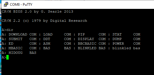
I can't find any use of the string "Close error" in the BIOS file. Does it come out of the CPM code? I wonder if I broke the card with bad writes? I think I will try the card in one of the FPGA boards that have an SD interface that works. Here's what the directory looks like from on the FPGA card within PuTTY.
CP/M BIOS 2.0 by G. Searle 2013

CP/M 2.2 (c) 1979 by Digital Research

A>dir
A: DOWNLOAD COM : LOAD     COM : PIP      COM : STAT     COM
A: SUBMIT   COM : DDT      COM : DISPLAY  COM : DUMP     COM
A: ED       COM : ASM      COM : BBCBASIC COM : POWER    COM
A: MBASIC   COM : BAS      BAS : BLINKLED BAS : blinkled bas
A: 0@@@  : .@@@  : 2@@@  : 2@@@
A:   : MYBAS4   BAS
A>
So, I was able to write to the card from the FPGA CP/M machine. Not sure yet what the difference is. There are more files than shown above which only show up in the VGA display for the FPGA card. PuTTY must filter them out.
Writes must be at least partly working since the directory does have the added items. But they are wrong. Not sure what it would take to clean up the card since it's not accessible from Windoze being formatted as a CP/M card.
The error is probably coming out of the function, CLOSEIT: which is found in the CPM22.LST file.
Looked up the XOR A instruction and found it does an XOR of itself so it will always return a status of 0. So I'm even more sure that it's not the block write command which is returning an error.
However, a bad block write could cause the error at a higher level in CP/M if the write didn't work properly. And I've still not verified the write worked properly so back to the PSoC monitor code that I used to test the read blocks. Adding a command to write a pattern to a block which can then be read by the read block routine. But I probably should use a block which is above the 128MB region of the disk drives.
128MB/512 bytes per block would be block 256K or block 0x4000. The SD card is 2 GB so I think I'll work with the block at 1 GB to be safe. Hopefully I won't kill the card, but if I do I have several other cards.
I've got another reason to think it's the SD write routine because of the directory being messed up. There has to be some difference between the block read which seems to work and the block write which sorta works.
Long enough for now, so I will be picking this up in the next log post.
-
Added Real Time Clock
10/26/2019 at 11:27 • 0 commentsAdded support for the Real Time Clock (RTC). The Z80_PSOC board has a spot for an optional 32.768 KHz watch crystal which provides accurate time.
The PSoC has internal circuitry for a clock. The board also has a battery holder so that the RTC is maintained when the main power is removed from the board.
RTC Access from the Z80
I added access from the Z80 to the Real Time Clock functions. The RTC addresses can be located at any 2 locations in the I/O Space. I put these addresses into the file HardwareConfig.h as:
#define RTC_DATA    0x60    // 96 dec
#define RTC_CSR     0x61    // 97 dec
The first location, RTC_DATA is the RTC Data location. The other location, RTC_CSR is the control/status register for the RTC.
The code for the clock is in Z80_RTC.c and .h files. The files implement a simple state machine to set and track the state of the clock interface. The states are in an enumeration as:
enum rtcStates
{
    RTC_SEC,    // 0
    RTC_MIN,    // 1
    RTC_HR,     // 2
    RTC_DAY,    // 3
    RTC_MON,    // 4
    RTC_YR_HI,  // 5
    RTC_YR_LO   // 6
};
The initialization code sets the first access to the seconds and turns on the clock. After reading the RTC_DATA from the code, the second access will automatically be set to the minutes. This continues on through the seven values. After the last location is read/written the state machine will go back to seconds.
Writing to the RTC_CSR location sets the offset to any of the fields. Values need to be limited to 0-6 matching the field offset. Reading the RTC_CSR location returns the the current state pointer.
Setting the RTC from BASIC
Setting the RTC code looks like this:
5 REM SET THE CLOCK POINTER TO SECONDS
10 OUT 97,0
20 REM SEC
30 OUT 96,1
40 REM MIN
50 OUT 96,35
60 REM HOUR
70 OUT 96,8
80 REM DAY
90 OUT 96,25
100 REM MON
110 OUT 96,10
120 REM YR_LO
130 OUT 96,227
140 REM YR_HI
150 OUT 96,7
BASIC uses integer math so the values are simple integers. The only complicated part is setting the year since it's a 16-bit value and has to be set in 2 parts. Setting the upper byte of the year to 7 sets the clock to 7*256=1792. Adding 227+1792 sets the year to 2019.
Reading the RTC from BASIC
The code to read the RTC is similar:
400 OUT 97,0
410 SC = INP(96)
420 MN = INP(96)
430 HR = INP(96)
440 DY = INP(96)
450 MO = INP(96)
460 YL = INP(96)
470 YH = INP(96)
480 PRINT "YR";((YH*256)+YL);"MON";MO;"DAY";DY;"TIME";HR;MN;SC
When RUN 400 is entered and looping, the clock returns:
YR 2019 MON 10 DAY 27 TIME 20  16  17
YR 2019 MON 10 DAY 27 TIME 20  16  17
YR 2019 MON 10 DAY 27 TIME 20  16  17
YR 2019 MON 10 DAY 27 TIME 20  16  18
The hours is a 24 hour (Military style) clock. Subtracting 12 from numbers over 12 and adding an AM/PM indication could be done.
PSoC Code Implemetation
As mentioned there is a driver Z80_RTC.c and .h that maps the Z80 accesses to the RTC code generated from the PSoC API generator. Setting the value works like this:
///////////////////////////////////////////////////////////////////////////////
// void writeRTC(uint8) - Write to RTC
// Auto-increment to the next field

void writeRTC(void)
{
    uint16 year;
    uint16 year2;
    uint8 wrVal = Z80_Data_Out_Read();

    switch (rtcState)
    {
        case RTC_SEC:
            RTC_WriteSecond(wrVal);
            rtcState = RTC_MIN;
            break;
        case RTC_MIN:
            RTC_WriteMinute(wrVal);
            rtcState = RTC_HR;
            break;
        case RTC_HR:
            RTC_WriteHour(wrVal);
            rtcState = RTC_DAY;
            break;
        case RTC_DAY:
            RTC_WriteDayOfMonth(wrVal);
            rtcState = RTC_MON;
            break;
        case RTC_MON:
            RTC_WriteMonth(wrVal);
            rtcState = RTC_YR_LO;
            break;
        case RTC_YR_LO:
            year = wrVal;
            RTC_WriteYear(year);
            rtcState = RTC_YR_HI;
            break;
        case RTC_YR_HI:
            year = RTC_ReadYear() + (wrVal<<8);
            RTC_WriteYear(year);
            rtcState = RTC_SEC;
            break;
    }
    ackIO();
}
Reading the RTC is driven by the same state bits and the code looks like this:
/////////////////////////////////////////////////////////////////////////////// // uint8 readRTC() - Read RTC // Auto-increment to the next field void readRTC(void) { uint8 retVal = 0; switch (rtcState) { case RTC_SEC: retVal = RTC_ReadSecond(); rtcState = RTC_MIN; break; case RTC_MIN: retVal = RTC_ReadMinute(); rtcState = RTC_HR; break; case RTC_HR: retVal = RTC_ReadHour(); rtcState = RTC_DAY; break; case RTC_DAY: retVal = RTC_ReadDayOfMonth(); rtcState = RTC_MON; break; case RTC_MON: retVal = RTC_ReadMonth(); rtcState = RTC_YR_LO; break; case RTC_YR_LO: retVal = (uint8)(RTC_ReadYear() & 0xff); rtcState = RTC_YR_HI; break; case RTC_YR_HI: retVal = (uint8)(RTC_ReadYear() >> 8); rtcState = RTC_SEC; break; } Z80_Data_In_Write(retVal); ackIO(); } -
Z80 (CP/M) Writing to SD Card
10/25/2019 at 11:06 • 0 commentsDigging into SD card writes means shifting gears from the Boot BIOS source code since the Boot BIOS code only does reads. The CP/M BIOS code (CBIOS128.LST) which does the reads/writes after booting. Here's the BIOS code for writes to the SD Card:
0754   EAC4             ;================================================================================================
0755   EAC4             ; Write physical sector to host
0756   EAC4             ;================================================================================================
0757   EAC4
0758   EAC4             writehst:
0759   EAC4 F5                  PUSH     AF
0760   EAC5 C5                  PUSH     BC
0761   EAC6 E5                  PUSH     HL
0762   EAC7
0763   EAC7 DB 89       wrWait1: IN    A,(SD_STATUS)
0764   EAC9 FE 80               CP    128
0765   EACB 20 FA               JR    NZ,wrWait1
0766   EACD
0767   EACD CD 2B EA            CALL     setLBAaddr
0768   EAD0
0769   EAD0 3E 01               LD    A,$01    ; 01 = Write block
0770   EAD2 D3 89               OUT    (SD_CONTROL),A
0771   EAD4
0772   EAD4 0E 04               LD     c,4
0773   EAD6 21 D2 FB            LD     HL,hstbuf
0774   EAD9             wr4secs:
0775   EAD9 06 80               LD     b,128
0776   EADB             wrByte:
0777   EADB
0778   EADB DB 89       wrWait2: IN    A,(SD_STATUS)
0779   EADD FE A0               CP    160 ; Write buffer empty
0780   EADF 20 FA               JR    NZ,wrWait2
0781   EAE1
0782   EAE1 7E                  LD     A,(HL)
0783   EAE2 D3 88               OUT    (SD_DATA),A
0784   EAE4 23                  INC     HL
0785   EAE5 05                  dec     b
0786   EAE6 20 F3               JR     NZ, wrByte
0787   EAE8
0788   EAE8 0D                  dec     c
0789   EAE9 20 EE               JR     NZ,wr4secs
The command to write to the SD card is 0x01. This is distinguished from reads which have a command of 0x00. The function SDWriteCommand( ) needs to call the read SD function or write SD function depending on the value.
The status value will require some thought. Here's the three values used by the sector read and sector write functions under the Z80 FPGA version of CP/M:
- 0x80 (128 dec) - SD interface is busy
- 0xE0 (224 dec) - Byte read in progress
- 0xA0 (160 dec) - Byte write empty
CP/M sectors are 128-bytes. Grant's code performed a tradeoff and set the sector size to 512-bytes. That's taken care of with the wr4secs loop.
I messed around with the status values and got writes partly working (at least not hanging). I got this:
>RUN
>SAVE "MY.BAS"

Close error
>BYE
And the directory looks messed up:
A>dir
A: DOWNLOAD COM : LOAD     COM : PIP      COM : STAT     COM
A: SUBMIT   COM : DDT      COM : DISPLAY  COM : DUMP     COM
A: ED       COM : ASM      COM : BBCBASIC COM : POWER    COM
A: MBASIC   COM : BAS      BAS : BLINKLED BAS : blinkled bas
A: 0@@@  : .@@@  : 2@@@  : 2@@@
I think I'll go back to the PSoC debugger side. First I need to create a new SD so that I don't mess up this one.
I did copy the 128MB disk using HxD and should be able to re-create it again if I had to.
-
SD Cards - PSoC to Z80
10/25/2019 at 08:58 • 0 commentsNow that we can read SD cards and have an I/O interface in place from the Z80 to do I/O mapped access to the SD card it's time to hook the two pieces together. To do this we will need to look closer at how Grant's code request blocks.
The loader code reads the status register SD_STATUS until the D7 bit is set.
The code then calls setLBAaddr.
It the writes to SD_CONTROL with 0x00 which causes the block read.
0584   026E             ;================================================================================================
0585   026E             ; Read physical sector from host
0586   026E             ;================================================================================================
0587   026E
0588   026E             readhst:
0589   026E F5                  PUSH     AF
0590   026F C5                  PUSH     BC
0591   0270 E5                  PUSH     HL
0592   0271
0593   0271 DB 89       rdWait1: IN    A,(SD_STATUS)
0594   0273 FE 80               CP    128
0595   0275 20 FA               JR    NZ,rdWait1
0596   0277
0597   0277 CD 5E 02            CALL     setLBAaddr
0598   027A
0599   027A 3E 00               LD    A,$00    ; 00 = Read block
0600   027C D3 89               OUT    (SD_CONTROL),A
0601   027E
0602   027E 0E 04               LD     c,4
0603   0280             ;        LD     HL,hstbuf
0604   0280             rd4secs:
0605   0280 06 80               LD     b,128
0606   0282             rdByte:
0607   0282
0608   0282 DB 89       rdWait2: IN    A,(SD_STATUS)
0609   0284 FE E0               CP    224    ; Read byte waiting
0610   0286 20 FA               JR    NZ,rdWait2
0611   0288
0612   0288 DB 88               IN    A,(SD_DATA)
Got it booting CP/M from the SD Card.
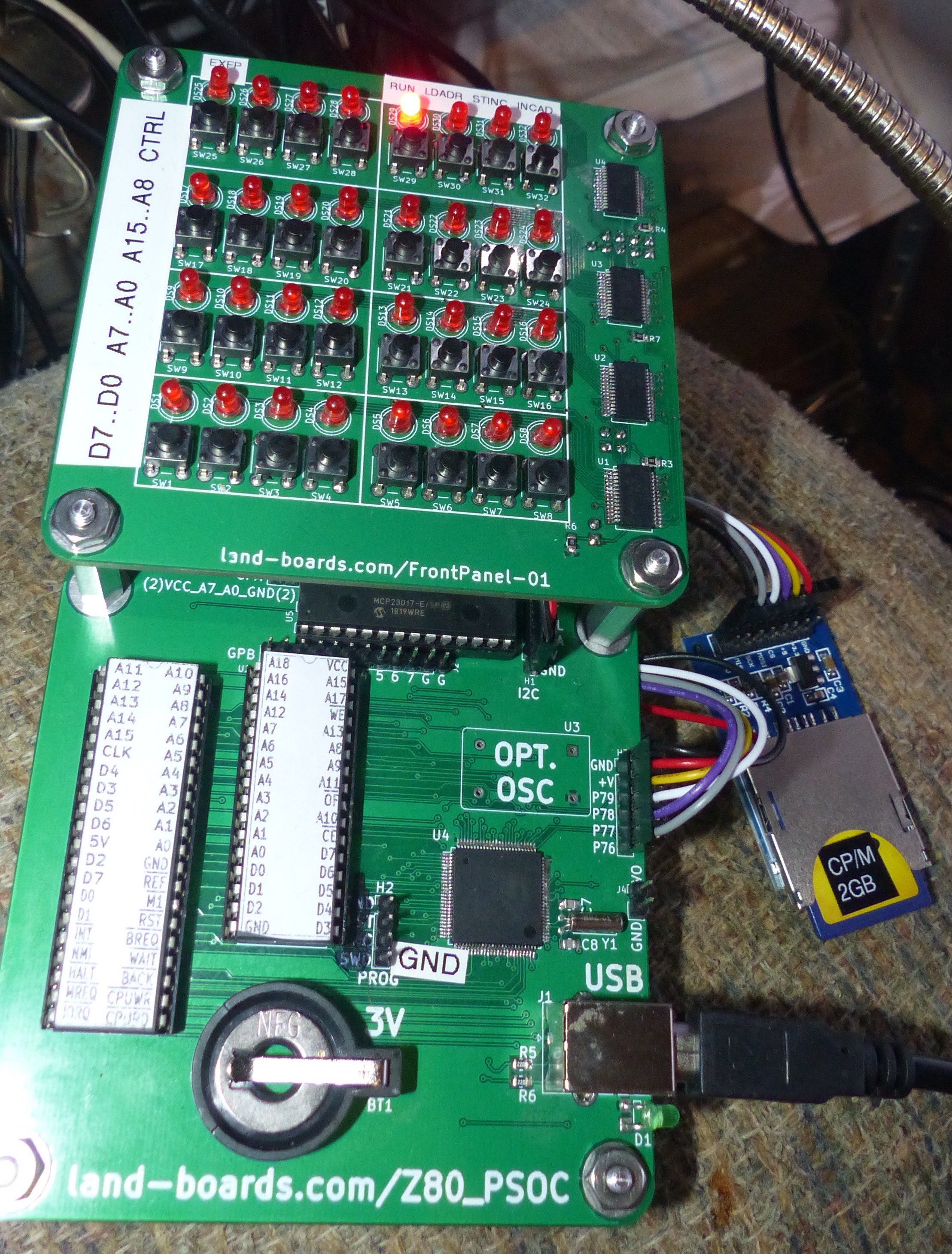
Here's the SD card attached to the Z80_PSOC.
![]()
Hooray!
Still need to get writes to the SD Card working.
-
Access SD Cards from the PSoC
10/24/2019 at 16:51 • 0 commentsI'm going to create a stand-alone PSoC project to use the PSoC to read SD cards. I'm going to start with the hardware defines for this project (which should leave the Z80 hardware pins unmolested) and just not download code.
For the software piece, I will add parts of the code I created to test the I2C EEPROM on our Not Quite Useless Raspberry Pi. This log entry covers that function. The code for that project reads the EEPROM on a Raspberry Pi hat and dumps it to the USB-Serial port for display on the PC in a serial terminal (PuTTY). The portion of that code that I want to copy is the dump of a PSoC memory buffer to the serial port as well as a bit of the command processor.
The goal is to dump the contents of the SD card in 512-byte sectors at a time to the USB-Serial and view it with PuTTY. We should also be able to view the SD card contents with HxD (described in a previous log post) and see that we got the right data.
It is tempting to do a straight port of the example code from the previous example which writes a byte at a time to the SPI interface and manually controls the Slave Select line. The I2C bus has support for reading data into a buffer or writing a buffer worth of data out automatically.
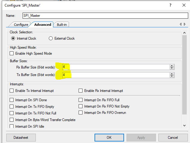
The Cypress datasheet for the SPI master lists the API functions that the PSOC Creator supports. In fact, PSOC Creator auto-generates these API so there's no effort required to create them. There is some support for putting an array of data into the transmit buffer - the function is SPIM_PutArray( ). There is also a PSOC 6 design example in the MCU SPI Master for performing SPI using Low-Level DMA but the symbol doesn't have rx_dma and tx_dma pins in the PSOC Creator for PSOC 5 parts.
It is worth noting that there are Rx and Tx Buffers built into the SPI master. The default depth is 4 bytes for each. This should be enough to have gap-less data transmit and receive.
The interface could also be interrupt driven but I don't see it as a problem if the Z80 ends up waiting on the SD card. The 512 byte block from the SD card can be read by the PSoC into a receive block. The Z80 is waiting around for data anyway. The entire block can be read into PSoC memory and then the status returned to the Z80 that there is data present.
The same applies to the 512 byte block writes to the SD card. The write could return control control to the Z80 as soon as it is written and the Z80 could go about it's business while the block finishes the write.All of this means that transfers to/from the SD card will be done through 512-byte buffers in the PSoC internal RAM. Writes from the Z80 will be to the transmit block and after the last byte is written from the Z80, the block will be transferred to the SD card. Reads from the Z80 will wait on the block to be completely read before returning status to the Z80 that receive data from the SD card is ready.
To begin with we only have to support reads so we will ignore SD card writes for the first cut.
PSoC Monitor Program
Up to this point the PSoC just runs the code to communicate with the Z80. For these next steps let's add a monitor program to run in place of the Z80 control. But how can we invoke the monitor program and not run the Z80 Peripheral Emulation? After all, we will want control of the USB-Serial interface and it's currently owned by the SIO/M6850 emulator when the Z80 is used.
The upper left button on the Front Panel exits the Front Panel code without releasing the reset to the Z80. We will use this feature to run monitor code that leaves the Z80 in reset and lets us test the SD card interface. To make use of this we will add a return value to the runFrontPanel( ) function. The return value will indicate to main( ) that we exited the Front Panel function without releasing reset.
Then we replicate the forever current loop in main( ) with a loop that handles the USB-Serial and runs a simple command driven menu. Fortunately, I created this code recently for our Not Quite Useless Raspberry Pi. Changing the code to not read EEPROM but instead read the SD card gets us what we want.
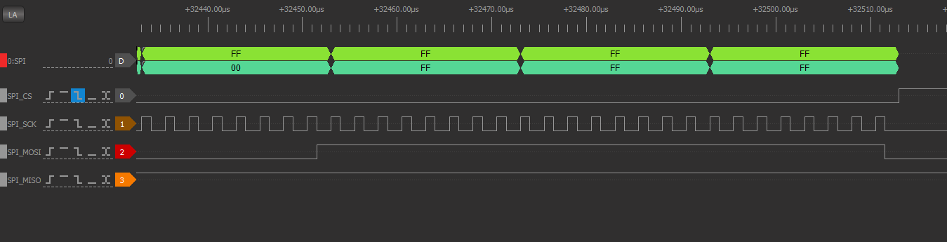
Here's a dummy block as read by the new PSoC Monitor Program:
Read from the SD Card
0000  00 01 02 03 04 05 06 07 08 09 0a 0b 0c 0d 0e 0f  ................
0010  10 11 12 13 14 15 16 17 18 19 1a 1b 1c 1d 1e 1f  ................
0020  20 21 22 23 24 25 26 27 28 29 2a 2b 2c 2d 2e 2f  .!"#$%&'()*+,-./
0030  30 31 32 33 34 35 36 37 38 39 3a 3b 3c 3d 3e 3f  0123456789:;<=>?
0040  40 41 42 43 44 45 46 47 48 49 4a 4b 4c 4d 4e 4f  @ABCDEFGHIJKLMNO
0050  50 51 52 53 54 55 56 57 58 59 5a 5b 5c 5d 5e 5f  PQRSTUVWXYZ[\]^_
0060  60 61 62 63 64 65 66 67 68 69 6a 6b 6c 6d 6e 6f  `abcdefghijklmno
0070  70 71 72 73 74 75 76 77 78 79 7a 7b 7c 7d 7e 7f  pqrstuvwxyz{|}~.
0080  80 81 82 83 84 85 86 87 88 89 8a 8b 8c 8d 8e 8f  ................
0090  90 91 92 93 94 95 96 97 98 99 9a 9b 9c 9d 9e 9f  ................
00a0  a0 a1 a2 a3 a4 a5 a6 a7 a8 a9 aa ab ac ad ae af  ................
00b0  b0 b1 b2 b3 b4 b5 b6 b7 b8 b9 ba bb bc bd be bf  ................
00c0  c0 c1 c2 c3 c4 c5 c6 c7 c8 c9 ca cb cc cd ce cf  ................
00d0  d0 d1 d2 d3 d4 d5 d6 d7 d8 d9 da db dc dd de df  ................
00e0  e0 e1 e2 e3 e4 e5 e6 e7 e8 e9 ea eb ec ed ee ef  ................
00f0  f0 f1 f2 f3 f4 f5 f6 f7 f8 f9 fa fb fc fd fe ff  ................
0100  00 01 02 03 04 05 06 07 08 09 0a 0b 0c 0d 0e 0f  ................
0110  10 11 12 13 14 15 16 17 18 19 1a 1b 1c 1d 1e 1f  ................
0120  20 21 22 23 24 25 26 27 28 29 2a 2b 2c 2d 2e 2f  .!"#$%&'()*+,-./
0130  30 31 32 33 34 35 36 37 38 39 3a 3b 3c 3d 3e 3f  0123456789:;<=>?
0140  40 41 42 43 44 45 46 47 48 49 4a 4b 4c 4d 4e 4f  @ABCDEFGHIJKLMNO
0150  50 51 52 53 54 55 56 57 58 59 5a 5b 5c 5d 5e 5f  PQRSTUVWXYZ[\]^_
0160  60 61 62 63 64 65 66 67 68 69 6a 6b 6c 6d 6e 6f  `abcdefghijklmno
0170  70 71 72 73 74 75 76 77 78 79 7a 7b 7c 7d 7e 7f  pqrstuvwxyz{|}~.
0180  80 81 82 83 84 85 86 87 88 89 8a 8b 8c 8d 8e 8f  ................
0190  90 91 92 93 94 95 96 97 98 99 9a 9b 9c 9d 9e 9f  ................
01a0  a0 a1 a2 a3 a4 a5 a6 a7 a8 a9 aa ab ac ad ae af  ................
01b0  b0 b1 b2 b3 b4 b5 b6 b7 b8 b9 ba bb bc bd be bf  ................
01c0  c0 c1 c2 c3 c4 c5 c6 c7 c8 c9 ca cb cc cd ce cf  ................
01d0  d0 d1 d2 d3 d4 d5 d6 d7 d8 d9 da db dc dd de df  ................
01e0  e0 e1 e2 e3 e4 e5 e6 e7 e8 e9 ea eb ec ed ee ef  ................
01f0  f0 f1 f2 f3 f4 f5 f6 f7 f8 f9 fa fb fc fd fe ff  ................
his code dumps a 512-byte block which is filled with dummy values. These dummy values will be replaced by the real data from from the SD Card. The block is read by pressing "R" on the PuTTY terminal.
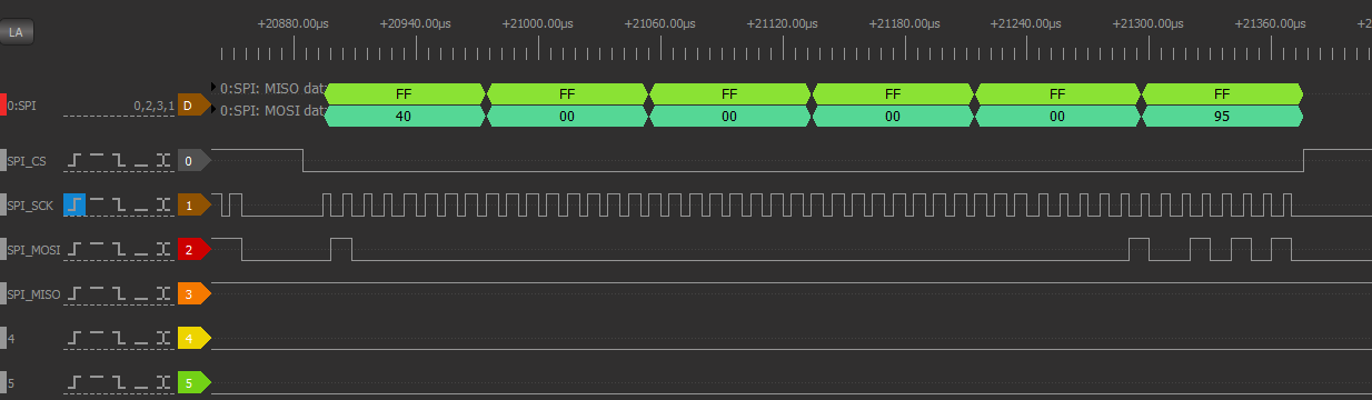
Block Read Command
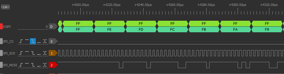
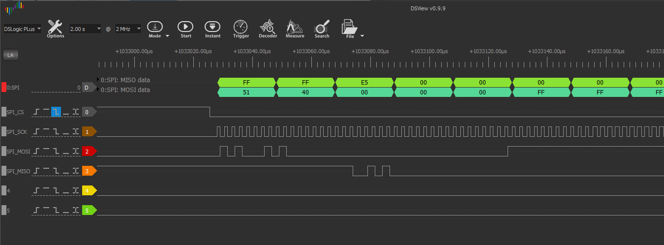
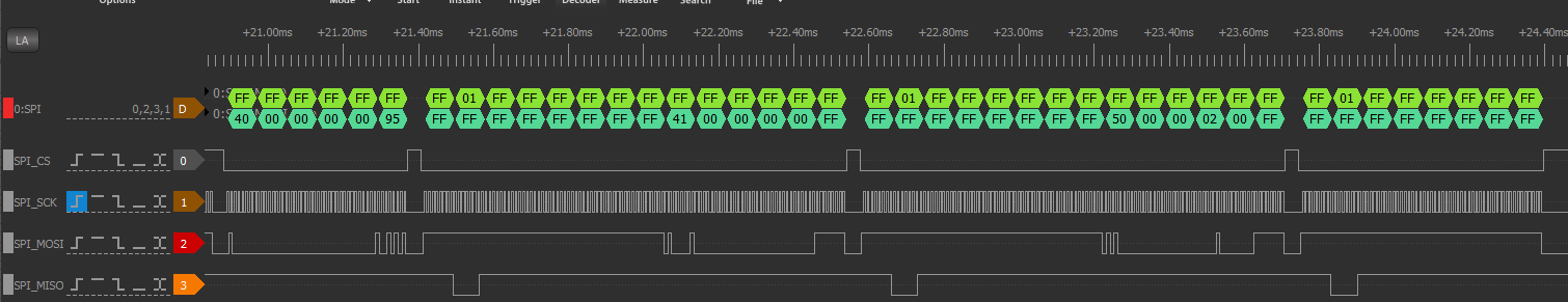
Here's a Logic Analyzer capture of the initialization pulses.Here's the 0x40 command.
Here's the status polling sequence.
The 0x01 shows up in the sequence which confirms the card status is ready.
Here's the 0x40, 0x41 and 0x50 sequence along with the card responses.
That is the initialization sequence for the card. The 0x1 status values show that the card is responding. The Bus Pirate version of the read sector command is:
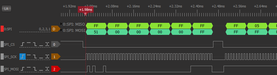
Read sector:
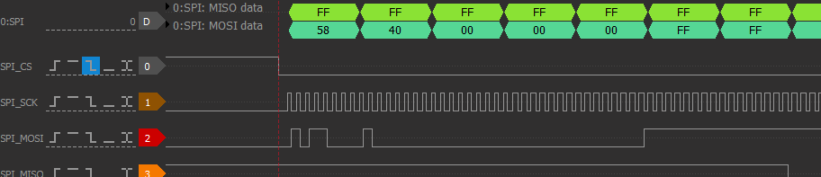
[0x51 0x00 0x00 0x00 0x00 0xFF r:520]The read sector command is the same as the above commands except it reads back 512 bytes.
The example code from the tutorial has the following C code:
void SD_read(unsigned long sector, unsigned short offset, unsigned char * buffer, unsigned short len) {
    unsigned short i, pos = 0;

    CS_ENABLE();
    SPI_write(0x51);
    SPI_write(sector>>15); // sector*512 >> 24
    SPI_write(sector>>7);  // sector*512 >> 16
    SPI_write(sector<<1);  // sector*512 >> 8
    SPI_write(0);          // sector*512
    SPI_write(0xFF);

    for(i=0; i<100 && SPI_write(0xFF) != 0x00; i++) {} // wait for 0

    for(i=0; i<100 && SPI_write(0xFF) != 0xFE; i++) {} // wait for data start

    for(i=0; i<offset; i++) // "skip" bytes
        SPI_write(0xFF);

    for(i=0; i<len; i++) // read len bytes
        buffer[i] = SPI_write(0xFF);

    for(i+=offset; i<512; i++) // "skip" again
        SPI_write(0xFF);

    // skip checksum
    SPI_write(0xFF);
    SPI_write(0xFF);

    CS_DISABLE();
}
My code is similar but doesn't slice up the data into a small buffer.
    ///////////////////////////////////////////////////////////////////////////////
    // void SD_readSector(uint32 sector, uint8 * buffPtr)

    void SD_readSector(uint32 sector, uint8 * buffPtr)
    {
        uint16 loopCount = 0;
        uint8 junk;
        SPI_write(0x51);
        SPI_write(sector>>15);
        SPI_write(sector>>7);
        SPI_write(sector<<1);
        SPI_write(0);
        SPI_write(0xFF);
        while((SPI_Master_ReadTxStatus() & SPI_Master_TX_FIFO_CLR) != SPI_Master_TX_FIFO_CLR);
        CyDelayUs(20);
        // wait for 0
        for(loopCount=0; loopCount<100; loopCount++)
        {
            SPI_write(0xFF);
            while ((SPI_Master_ReadRxStatus() & SPI_Master_RX_FIFO_CLR) == SPI_Master_RX_FIFO_CLR);
            if (SPI_Master_ReadRxData() == 0)
                break;
        }
        // wait for 0xFE
        for(loopCount=0; loopCount<100; loopCount++)
        {
            SPI_write(0xFF);
            while ((SPI_Master_ReadRxStatus() & SPI_Master_RX_FIFO_CLR) == SPI_Master_RX_FIFO_CLR);
            if (SPI_Master_ReadRxData() == 0xFE)
                break;
        }
        for(loopCount=0; loopCount<512; loopCount++)
        {
            SPI_write(0xFF);
            while ((SPI_Master_ReadRxStatus() & SPI_Master_RX_FIFO_CLR) == SPI_Master_RX_FIFO_CLR);
            buffPtr[loopCount] = SPI_Master_ReadRxData();
        }

        SPI_write(0xFF);
        while ((SPI_Master_ReadRxStatus() & SPI_Master_RX_FIFO_CLR) == SPI_Master_RX_FIFO_CLR);
        junk = SPI_Master_ReadRxData();

        SPI_write(0xFF);
        while ((SPI_Master_ReadRxStatus() & SPI_Master_RX_FIFO_CLR) == SPI_Master_RX_FIFO_CLR);
        junk = SPI_Master_ReadRxData();

        return;
    }
My SD card is returning a "bad" status. Rather than 0x00, it is returning 0x05.
So near, and yet so far.
Slept on It
Slept for a while and decided to check the SD_init( ) code from the fat88.c code. It's got delays between commands. The bus pirate manual commands would have had time delays due to entering the commands by hand. The code has:
char SD_init() {
	char i;

	// ]r:10
	CS_DISABLE();
	for(i=0; i<10; i++) // idle for 1 bytes / 80 clocks
		SPI_write(0xFF);

	// [0x40 0x00 0x00 0x00 0x00 0x95 r:8] until we get "1"
	for(i=0; i<10 && SD_command(0x40, 0x00000000, 0x95, 8) != 1; i++)
		_delay_ms(100);

	if(i == 10) // card did not respond to initialization
		return -1;

	// CMD1 until card comes out of idle, but maximum of 10 times
	for(i=0; i<10 && SD_command(0x41, 0x00000000, 0xFF, 8) != 0; i++)
		_delay_ms(100);

	if(i == 10) // card did not come out of idle
		return -2;

	// SET_BLOCKLEN to 512
	SD_command(0x50, 0x00000200, 0xFF, 8);

	sd_sector = sd_pos = 0;

	return 0;
}
Changed my SD_init( ) code to match:
    void SDInit(void)
    {
        uint8 iter;
        // Dummy fill the read/write buffers
        for (uint16 loopCount=0; loopCount<512; loopCount++)
        {
            readSDBuffer[loopCount] = (uint8)loopCount;
            writeSDBuffer[loopCount] = ~(uint8)loopCount;
        }

        // p 5 of http://www.dejazzer.com/ee379/lecture_notes/lec12_sd_card.pdf
        //
        // https://codeandlife.com/2012/04/25/simple-fat-and-sd-tutorial-part-3/
        // Init and go to SPI mode: ]r:10 [0x40 0x00 0x00 0x00 0x00 0x95 r:8]

        // Send at least 74 clocks with SS and MOSI high
        SPI_SS_Override_Write(1);                   // Force SPI_SS line high
        SPI_Master_Start();
        for (uint8 loopCount = 0; loopCount < 10; loopCount++)
        {
            while ((SPI_Master_ReadTxStatus() & SPI_Master_STS_TX_FIFO_NOT_FULL) == 0);
            SPI_Master_WriteTxData(0xff);   // Hang around while the FIFO is full
        }
        // Wait around for the FIFO to get empty
        while((SPI_Master_ReadTxStatus() & SPI_Master_TX_FIFO_CLR) != SPI_Master_TX_FIFO_CLR);
        SPI_SS_Override_Write(0);                   // Allow the SPI_Master to control the SPI_SS line
        CyDelayUs(10);
        SPI_Master_ClearRxBuffer();

        // Initialize card: [0x41 0x00 0x00 0x00 0x00 0xFF r:8]
    	for(iter=0; iter<10 && SD_command(0x40, 0x00000000, 0x95, 8) != 1; iter++)
    		CyDelay(100);

        // Set transfer size: [0x50 0x00 0x00 0x02 0x00 0xFF r:8]
    	for(iter=0; iter<10 && SD_command(0x41, 0x00000000, 0xFF, 8) != 0; iter++)
    		CyDelay(100);

        // Read sector: [0x51 0x00 0x00 0x00 0x00 0xFF r:520]
        SD_command(0x50, 0x00000200, 0xFF, 8);

        // Initialize the Z80 interface
        SD_DataOut = 0x0;
        SD_DataIn = 0x0;
        SD_Status = 0x0;
        SD_Command = 0x0;
        SD_LBA0_Val = 0x0;
        SD_LBA1_Val = 0x0;
        SD_LBA2_Val = 0x0;
        SD_LBA3_Val = 0x0;
    }
And it worked. Here's the dump of the start of the first sector of the SD card.
Land Boards, LLC - Z80_PSoC monitor
R - Read SD Card
? - Print this menu
Read from the SD Card
0000  c3 5c d3 c3 58 d3 7f 00 43 6f 70 79 72 69 67 68  .\..X...Copyrigh
0010  74 20 31 39 37 39 20 28 63 29 20 62 79 20 44 69  t.1979.(c).by.Di
0020  67 69 74 61 6c 20 52 65 73 65 61 72 63 68 20 20  gital.Research..
0030  20 20 20 20 00 00 00 00 00 00 00 00 00 00 00 00  ................
That was somewhat painful but made quite a bit easier by the tutorial. Thanks Joonas Pihlajamaa.
-
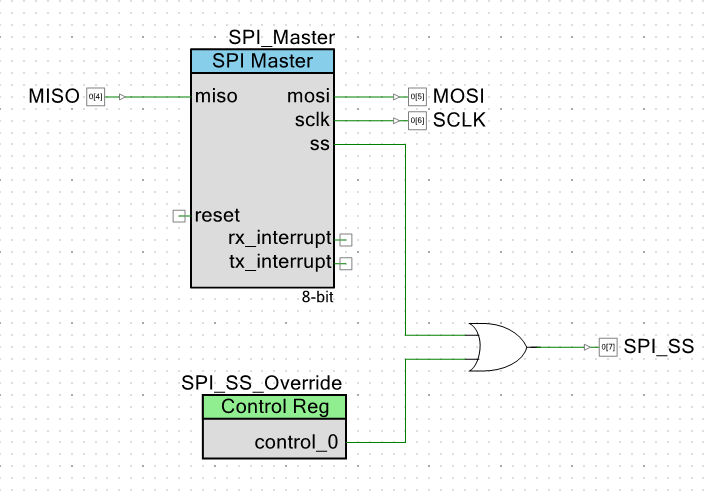
SPI Slave Select Change
10/24/2019 at 13:36 • 0 commentsI am changing my earlier approach to the SPI Slave Select (SS) line.
The SPI controller should be used to control the SS line. But as we saw earlier there's times when that value needs to be over-ridden. During the initialization there needs to be at least 72 SPI clocks with SS and MOSI both high. It is a problem to have the PSoC SPI_Master to do since the interface wants to assert SS for the entire transfer. But we want to use the SPI_Master to control the SPI interface under other circumstances.
Here is a way to achieve both of these goals.
The extra OR gate on the output lets the SPI_SS_Override control register over-ride the active-low Slave Select from the SPI_Master during just the initialization phase. Setting the bit to 1 will cause the SPI_SS pin to have a 1 overrides the SS from the SPI_Master. Setting the bit to 0 after the initialization cycle allows the SPI_Master to control the line normally.
This is one example of the flexibility of the PSoC approach. It's pretty easy to add hardware assistance to functions that would otherwise require more CPU attention. -
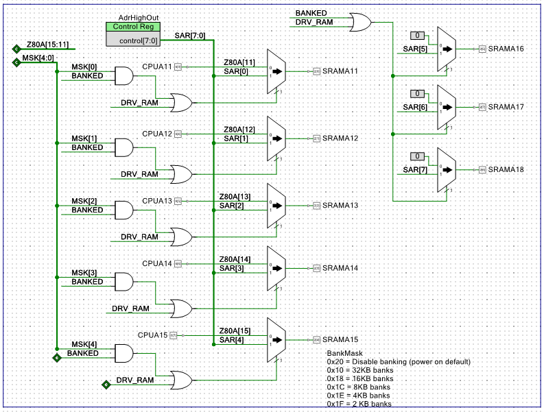
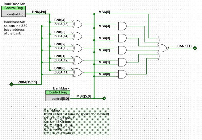
Changes to Bank Switch Logic
10/23/2019 at 21:34 • 0 commentsMade some changes to the address mapper/bank switch hardware to support Grant's bank switching.
Signals are:
- DRV_RAM - asserted when the PSoC was testing the SRAM at power up and when Z80 code is loaded into the SRAM to be run.
- MSK[4..0] determines whether the address is used when the bank SRAM is accessed.
- Z80A[15..11] is the address directly from the Z80.
- BankMask MSK[]4..0] is the number of bits that are replaced is determined by this.
- SRAMA[18..A16] are all zero's when the access is to spaces other than the bank.
- SRAMA[18..16] are set from the SAR[7..5] when the BANK is selected.
Set the Base Address for comparison to the first 8KB of SRAM which asserts the BANKED line.
Needed to add in the MSK bits into each individual address select mux. The BankMask is set to 0x1C for 8KB banks. That means that the Z80A11 and A10 bits are passed through directly and only when the address is in the range of the first 8KB is the selection from the AdrHighOut.
The Bank Base Address comparison logic looks like this.
With the previous logic the board rebooted when I did a cold boot.
After making these changes the board booted correctly. The Bank logic initialization code looks like this:
#define BANK_SIZE_32K   0x10
#define BANK_SIZE_16K   0x18
#define BANK_SIZE_8K    0x1c
#define BANK_SIZE_4K    0x1E
#define BANK_SIZE_2K    0x1F

// Memory Mapper version 1 sets bank size to 8KB
// Points to the first SRAM bank

void init_mem_map_1(void)
{
    BankBaseAdr_Write(0x00);
    BankMask_Write(BANK_SIZE_8K);
    AdrHighOut_Write(0x00);
}
This logic is pretty general purpose and could support multiple pages if the Z80 wrote to a bank select I/O address. Grant's code only goes a single swap of the spaces.
Grant's code only switches out the 8KB bank for another bank. This function does the switch:
/////////////////////////////////////////////////////////////////////////////////
// void swap_out_ROM_space(void) - When called switches to the 2nd bank
// Used with Memory Map 1 scheme where there's a single 8KB bank starting at 0x0000
// which is switched out when an I/O location is written.

void swap_out_ROM_space(void)
{
    AdrHighOut_Write(0x20);     // Set A18..A16 to 0x1
    ackIO();
}
Other memory maps would need their own functions, so I've bracketed the code with a #define to indicate it only applies to this software build.
The weakness of this scheme is that it really doesn't take good advantage of the extra memory. After all, we've got 512KB and are only using 64K + 16K = 80K of the 512KB. But for CP/M this is probably just fine.
Not an MMU
This isn't really quite an Memory Management Unit (MMU) since it would need to be able to swap multiple spaces rather than just one space. An MMU would take additional comparison logic as well as muxes to select the right addresses. Optimally this could be done with a fast RAM which would associate addresses from the Z80 to bank addresses on the output which would get routed to the SRAM as the upper address bits. The PSoC isn't optimal for this since the logic in the part is limited. But a few bank selects could be created which are basically just copies of the above logic plus additional multiplexer inputs.
One use of such a scheme would be to support a RAM disk. After all, the 512KB could be put to good use if it were made available. But this would take a bit of support from the CP/M code itself.
Grant has a 128KB version of CP/M which could be promising for this approach. May investigate later one.
3-Chip Z80 Design
Combining a Z80 retro design with a modern PSoC CPU.

 The interface could also be interrupt driven but I don't see it as a problem if the Z80 ends up waiting on the SD card. The 512 byte block from the SD card can be read by the PSoC into a receive block. The Z80 is waiting around for data anyway. The entire block can be read into PSoC memory and then the status returned to the Z80 that there is data present.
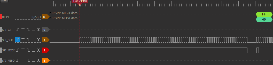
 The extra OR gate on the output lets the SPI_SS_Override control register over-ride the active-low Slave Select from the SPI_Master during just the initialization phase. Setting the bit to 1 will cause the SPI_SS pin to have a 1 overrides the SS from the SPI_Master. Setting the bit to 0 after the initialization cycle allows the SPI_Master to control the line normally.