land-boards.com
-
Z80 SIO Emulation (part 2)
10/11/2019 at 19:51 • 0 commentsSPoC Code Side
The PSoC will need to poll the IO_Stat_Reg and wait until it sees IORQ* asserted along with either CPURD* or CPUWR*. It should then read the AdrLowIn status register. Using this information, the PSoC should then perform the IO operation.
The main( ) code is actually not idle. It's essentially polling the USB interface. I think the USB is interrupt driven so the code probably just interacts with the handshake to the interrupt. It is currently configured to loop back USB data from the receive to the transmit. I can see this on the PC when I connect to the card using PuTTY. Whatever I type gets echoed back. This will need to be intercepted and routed to the Z80 via the SIO interface.
Data, Status and Ports
There are four pins provided for an external UART, but I'm going to just toss out the SIO data from the second part for the moment. Using the PSoC debugger to single step, the first write is to the SIO A Control Register with a value of 0. This matches the ASM code.
0403   01A6 3E 00               LD    A,$00
0404   01A8 D3 02               OUT    (SIOA_C),A
0405   01AA 3E 18               LD    A,$18
0406   01AC D3 02               OUT    (SIOA_C),A
SIO Data Sheet
This is when looking at the SIO data sheet comes into play. What does a write to the control register with a value of 0x0 do in the SIO?
The SIO is described in the document Z8420 Peripheral User Manual um0081 starting on p207. There's a lot of information in there about all of the modes that the SIO can do.
Grant's schematic connects the interrupt line from the SIO to the Z80 but that, by itself doesn't mean it is interrupt driven. The Monitor Code has the following:
0139   0062             ;------------------------------------------------------------------------------
0140   0062             ; Serial interrupt handlers
0141   0062             ; Same interrupt called if either of the inputs receives a character
0142   0062             ; so need to check the status of each SIO input.
0143   0062             ;------------------------------------------------------------------------------
0144   0062 F5          serialInt:    PUSH    AF
0145   0063 E5                  PUSH    HL
So, it looks like the hardware and code support interrupts. It looks like there may only be a receive buffer so the interrupts may only be on receive characters. I will have to dig deeper to see if that is the case. It does make sense to have interrupts on receive and wait on output since the buffer could just back up on the transmit side anyway if the host is not ready.
If it's the case that there's only input interrupts then I should be able to get outputs running without worrying about interrupt handling. The console output routine also seems to be polled and waits until the transmit is ready.
0287   0124             ;------------------------------------------------------------------------------
0288   0124             ; Console output routine
0289   0124             ; Use the "primaryIO" flag to determine which output port to send a character.
0290   0124             ;------------------------------------------------------------------------------
0291   0124 F5          conout:        PUSH    AF        ; Store character
0292   0125 3A 8A 40            LD    A,(primaryIO)
0293   0128 FE 00               CP    0
0294   012A 20 0D               JR    NZ,conoutB1
0295   012C 18 01               JR    conoutA1
0296   012E             conoutA:
0297   012E F5                  PUSH    AF
0298   012F
0299   012F CD 42 01    conoutA1:    CALL    CKSIOA        ; See if SIO channel A is finished transmitting
0300   0132 28 FB               JR    Z,conoutA1    ; Loop until SIO flag signals ready
0301   0134 F1                  POP    AF        ; RETrieve character
0302   0135 D3 00               OUT    (SIOA_D),A    ; OUTput the character
0303   0137 C9                  RET

...

0314   0142             ;------------------------------------------------------------------------------
0315   0142             ; I/O status check routine
0316   0142             ; Use the "primaryIO" flag to determine which port to check.
0317   0142             ;------------------------------------------------------------------------------
0318   0142             CKSIOA
0319   0142 97                  SUB    A
0320   0143 D3 02               OUT     (SIOA_C),A
0321   0145 DB 02               IN       A,(SIOA_C)    ; Status byte D2=TX Buff Empty, D0=RX char ready
0322   0147 0F                  RRCA            ; Rotates RX status into Carry Flag,
0323   0148 CB 4F               BIT      1,A        ; Set Zero flag if still transmitting character
0324   014A C9                      RET
The PSoC USB interface ought to be significantly faster than a Serial UART.
Some things, like bits per character, stop bits, parity don't matter for the USB-Serial interface since it's automatically taken care of by the USB transport so writes to those control values can be safely ignored (at least for the USB-Serial port). They will probably need to be taken into account for the 2nd UART interface, but a lot of that is easily handled by the PSoC UART code.
As a side note: M1* will matter when it comes to handling interrupts (from the SIO datasheet)
M1 Machine Cycle One (input from Z80 CPU, active Low). When M1 is
active and RD is also active, the Z80 CPU is fetching an instruction from
memory; when M1 is active while IORQ is active, the Z80 SIO accepts
M1 and IORQ as an interrupt acknowledge if the Z80 SIO is the highest
priority device that has interrupted the Z80 CPU.
Hardware handshake is also not an issue for the USB-Serial port since it's also taken care of by the USB protocol.
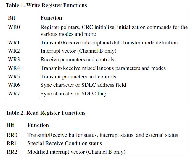
The SIO datasheet shows that there are multiple registers which apparently are selected by a write to the first location.
These registers can be represented in C by variables.
WR0
WR1:
Re-writing Grant's SIO initialization code as psuedo-code:
; SIO Initialization code in Grant's monitor
; Set up Port A
SIOA_C = $00        ; WR0
SIOA_C = $18        ; Channel A reset

SIOA_C = $04        ; Select WR4
SIOA_C = $C4        ; X64 clock rate, 1 stop bit, no parity

SIOA_C = $01        ; Select WR1
SIOA_C = $18        ; Rx int on all rx chars, no Tx int enable

SIOA_C = $03        ; Select WR3
SIOA_C = $E1        ; 8 bits/char, auto enable CTS, Rx Enable

SIOA_C = $05        ; Select WR5
SIOA_C = RTS_LOW    ; RTS = LOW

; Set up Port B
SIOB_C = $00        ; Select WR0
SIOB_C = $18        ; Channel A reset

SIOB_C = $04        ; Select WR4
SIOB_C = $C4        ; X64 clock rate, 1 stop bit, no parity

SIOB_C = $01        ; Select WR1
SIOB_C = $18        ; Rx int on all rx chars, no Tx int enable

SIOB_C = $02        ; Select WR2 is Interrupt Vector Register
SIOB_C = $60        ; INTERRUPT VECTOR ADDRESS Value

SIOB_C = $03        ; Select WR3
SIOB_C = $E1        ; 8 bits/char, auto enable CTS, Rx Enable

SIOB_C = $05        ; Select WR5
SIOB_C = RTS_LOW    ; RTS = LOW
I think I could simply ignore any writes to the control registers since I know what they do in Grant's code. This isn't a general purpose emulator, but I don't need to support many of the SCC modes. A more general purpose emulator would need to deal with changes to the registers. All I really need to know is:
- Receive characters are interrupt driven
- Transmit characters are directly written by polling status and then writing
The one thing I do need is the WR2 value since it provides the interrupt vector address. This get supplied back to the Z80 in response to an interrupt acknowledge cycle.
Another possibility is to hard code the fact that these accesses have to come in pairs. The first access is the offset to the register in the second access. I could stuff away the register values based on the second access and hard code this as pairs in the SIO emulator. This seems like the best choice.
-
Z80 SIO Emulation by the PSoC
10/11/2019 at 18:15 • 0 commentsThis is the real meat of this project. Beyond the advantages of compact design, front panel, loadable firmware, etc., getting Z80 peripherals to work is key. What good is something that will run code if it can't deliver output and read input?
Grant's 9-Chip Design
Grant only has three I/O addresses mapped in his design:
- SIO (Two Channel UART)
- Bank Switch for CP/M
- I/O connector
I am not supporting an external I/O connector. I've got something in mind for the bank switching but don't need it yet. Bank switching isn't needed to run BASIC. So the only thing left is to get SIO emulation working.
Addresses
According to the schematic notes, the SIO base address is 0x00-0x07. The address range is actually 4 addresses, not 8 addresses.
The lowest two address lines connect as follows:
- A0 = B/A*
- A1 = C/D*
A/B* selects between the two UARTS and C/D* selects between control and data. The monitor uses these addresses:
0071   0000             SIOA_D        .EQU    $00
0072   0000             SIOA_C        .EQU    $02
0073   0000             SIOB_D        .EQU    $01
0074   0000             SIOB_C        .EQU    $03
A very quick look makes me think that the BASIC relies on the monitor for I/O so there's no need to support A2 (addresses 0x04-0x07).
PSoC Polling the I/O Interface
My first cut is that the PSoc will monitor the IOREQ* line to handle I/O. The PSoC is doing nothing presently once the Front Panel routine is done.
A second cut could be to do this with interrupts, but I'm not going that way until polling works.
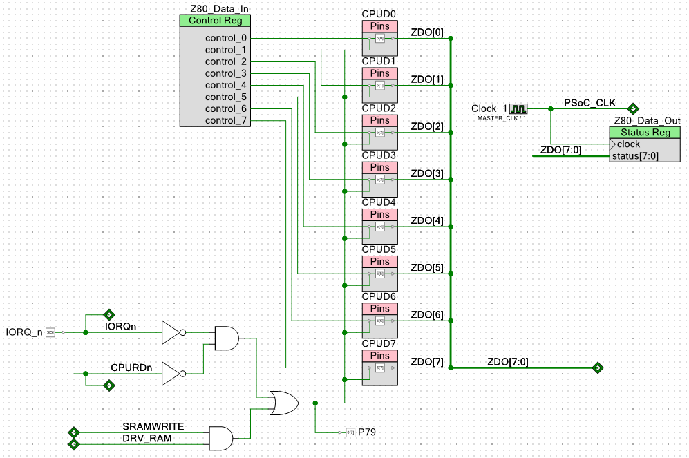
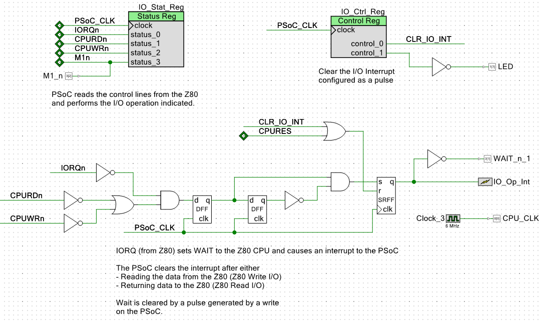
PSoC Z80 Peripheral Emulation Hardware
The hardware has a mailbox for communication with the Z80.
The data from the Z80 is clocked into the Z80_Data_Out status register which can be read by the PSoC. Writing to the Z80_Data_In control register from the PSoC will allow data to be returned to the Z80. Direction control (output enable to the Z80) is enabled when the Z80 asserts both IORQ* and CPURD*.
The controller is a bit more complicated. It asserts WAIT* when there's an I/O request and removes WAIT* when the transfer is complete.
The IO_Stat_Reg lets the PSoC read the values of the IORQ*, CPURD*, CPUWR* and M1* lines. The M1 value determines if the IO access is an interrupt acknowledge cycle or a regular I/O cycle.
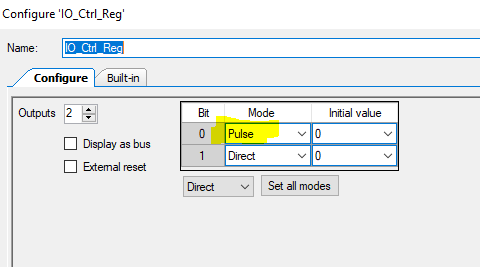
The IO_Ctrl_Reg is used to clear the IO Interrupt and deassert WAIT* by resetting the R-S flip flop. The d0 bit of the register is set up to cause a pulse when written which will deassert WAIT*. This is set up in the register configuration as:
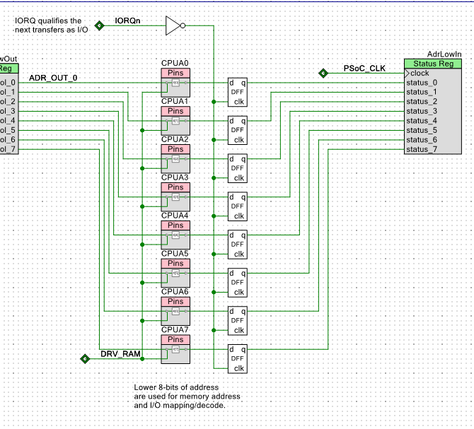
There's also a status register (AdrLowIn) that has the Z80 address lines A0-A7. The address is latched at the falling edge of IORQ*.
-
Z80 Pins and Debugging
10/11/2019 at 16:52 • 0 commentsThere are two ways to get to the Z80 bus for external operations.
- RESET* - Clears PC and sets address/data bus to Hi-Z
- BUSREQ* - input - Address, Data, MREQ*, IORQ*, RD*, WR* to HiZ
- BUSACK* - output indicates that BUSREQ* signal was performed (Hi-Z busses)
Other controls:
- HALT* - output
- A0-A15 - tristated by RESET*
- D0-D7 - tristated by RESET*
- BUSACK* - output
Debugging with Logic Analyzer
Looking at the lower address and data bits with the DSLogic+.
The data looks like the bottom nibble is stuck with 0x3 which does match the first instruction but it doesn't look like it's changing for the following instructions. Here's the first few lines of the assembly code:
unsigned char monitor_eprom[] =
{
0xF3, 0xC3, 0x8A, 0x01, 0x00, 0x00, 0x00, 0x00, 0xC3, 0x24, 0x01, 0x00,
0x00, 0x00, 0x00, 0x00, 0xC3, 0xC0, 0x00, 0x00, 0x00, 0x00, 0x00, 0x00,
The first two instructions do have 0x3 as the bottom nibble but the next lines don't. The start of the code has:
MON        .ORG    $0000        ; MONITOR ROM RESET VECTOR
;------------------------------------------------------------------------------
; Reset
;------------------------------------------------------------------------------
RST00        DI            ;Disable INTerrupts
        JP    INIT        ;Initialize Hardware and go
        NOP
        NOP
        NOP
        NOP
Looking at the Code
I want to look and see if the right stuff is running, but I don't have a listing file for the output of the assembler. I just have Grant's ASM source. Grant also includes the TASM assembler but it doesn't run under 64-bit windows.
I tried TASM in DOSBOX and it works. It needed all the files (TASM.*). I did that and the program created a list file automatically. Here's the first few lines of the listing:
0102   0000 F3          RST00        DI            ;Disable INTerrupts
0103   0001 C3 8A 01            JP    INIT        ;Initialize Hardware and go
0104   0004 00                  NOP
0105   0005 00                  NOP
0106   0006 00                  NOP
0107   0007 00                  NOP
INIT is:
0387   018A 31 AE 40    INIT        LD   SP,STACK        ; Set the Stack Pointer
0388   018D
0389   018D 21 00 40            LD    HL,serABuf
0390   0190 22 40 40            LD    (serAInPtr),HL
0391   0193 22 42 40            LD    (serARdPtr),HL
0392   0196
0393   0196 21 45 40            LD    HL,serBBuf
0394   0199 22 85 40            LD    (serBInPtr),HL
0395   019C 22 87 40            LD    (serBRdPtr),HL
0396   019F
0397   019F AF                  xor    a            ;0 to accumulator
0398   01A0 32 44 40            LD    (serABufUsed),A
0399   01A3 32 89 40            LD    (serBBufUsed),A
0400   01A6
0401   01A6             ;    Initialise SIO
0402   01A6
0403   01A6 3E 00               LD    A,$00
0404   01A8 D3 02               OUT    (SIOA_C),A
0405   01AA 3E 18               LD    A,$18
0406   01AC D3 02               OUT    (SIOA_C),A
Dumped the RST00 and INIT code with the Front Panel and the code matches the listing so I think it loaded correctly.
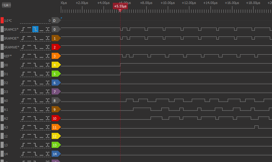
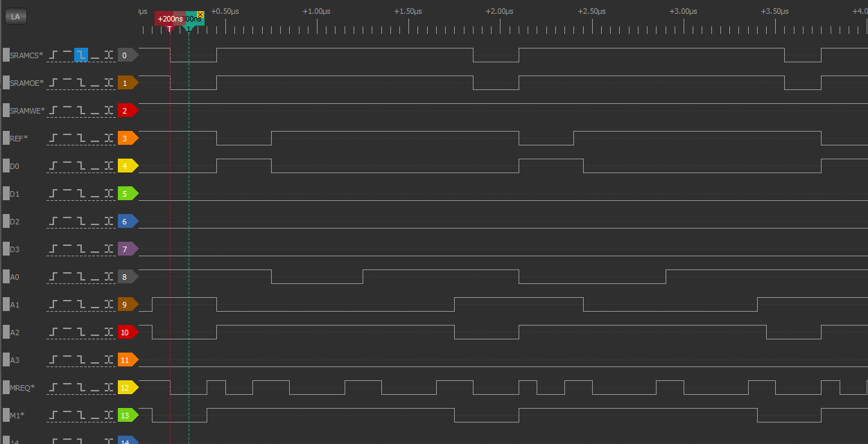
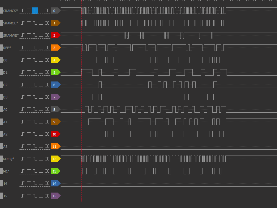
Added connection to M1* and MREQ*. MREQ* runs a lot more than I expected but it's not always qualified with M1*.
I found the problem - it is in the trace above. I was qualifying SRAMCS* with M1* being low. M1* is only low during the first byte of an instruction, ie, it's only active during the opcode fetch. I removed M1* from the equation and got this:
And IOREQ* is stuck low waiting on the PSoC to remove the WAIT*. The code runs about as long as I would expect given the number of instructions shown to reach address 0x01A8 where the IO OUT happens.
Confirmed that IOREQ* is low with the scope. First time I've seen it low!!!
Now, on to work on the SIO emulator...
-
Power Problems
10/11/2019 at 02:49 • 0 commentsThe USB hub I was using was only putting out 4.45V. The CMOS Z80 needs 4.5V (min). The PSoC isn't as picky about power. The core of the CPU is powered from a regulator inside the PSoC.
I plugged the USB cable into my PC and now I am getting a clean 5.04 V.
The CPU clock looks cleaner, now.
I need a better hub.
Still not producing IORQ* signal.
But getting closer.
-
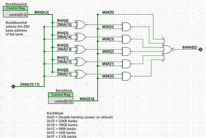
Banking When It Shouldn't
10/11/2019 at 02:10 • 0 commentsBanking was coming on by default.
Added bank control to shut off banking at power on.
Setting MSK[5] to default to '1' at power up. This should maked BANKED signal off.
BANKED was causing the map to be selected which was defaulted to zero. Hence, CPUA11 to CPUA15 was being over-ridden by the bank register value of 0x0.
It is not yet running but I do see the A14 and A15 address lines being passed through the PSoC.
-
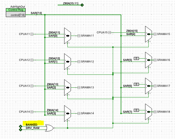
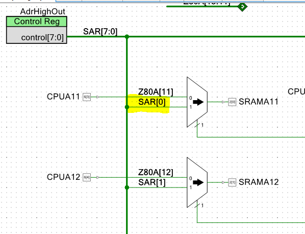
Fixed SRAM bug
10/11/2019 at 00:42 • 0 commentsI had a bug on SRAMA11. It manifested as an inability to set the line high. Actually, it was connected to SRAMA12 and when SRAM12 went high SRAMA11 also went high. Was incredibly easy to fix.
Problem manifested as a bad dump of the ROM file. I am using Grant's ROM.HEX file converted to a C array. Dumping at 0x0000 showed data from somewhere else. Board was passing SRAM test but the test looped data every 256 bytes. For some reason the address line shift test was passing (need to figure that out still).
Used Front Panel to set one address line at a time. Set the address I wanted with the LDADR button on the front panel. Looked with the scope at the affected address line. Found that SRAMA11 was tied to SRAMA12. It wasn't a short on the board, it was an error on the banking page of the schematic. This is the bit fixed but it was set to SAR[1] so it was replicating SRAMA12.
Now the dump of the ROM works. At least the first few locations look right. Need to check some additional locations to verify they work.
Using Grant's 9-chip ROM.HEX file. The file has both the basic and monitor in one 8KB ROM. From Grant's page:
ROM contents
ROM.HEX (all that is needed to program the ROM. Contains the BASIC.HEX and MONITOR.HEX)
Next step is to design the SIO emulator.
Running Grant's code I am not seeing any IORQ* strobes. I think I should be seeing IORQ* strobes.
I need simpler IO code.
-
Converting Grant's Hex files to C arrays
10/10/2019 at 02:08 • 0 commentsConvert basic hex file to C array:
srecord\srec_cat basic.hex -intel -o basic.c -C-ArrayConvert rom hex file to C array:
srecord\srec_cat rom.hex -intel -o rom.c -C-Array
The memory map on Grant's site:
MEMORY MAPS

INITIAL BOOT

0000-3FFF ROM
   Within the ROM...
      0x0000 Boot monitor
      0x2000 Microsoft BASIC interpreter
4000-FFFF RAM

Once CP/M is loaded

0000-FFFF RAM

0100 Transient program area (applications)
D000 CP/M System
E600 BIOS
So the boot code needs to be loaded into SRAM starting at 0 and the BASIC code needs to be loaded into SRAM starting at 0x2000.
-
Downloaded Code
10/10/2019 at 01:26 • 0 commentsI found a program, srecord, which turns HEX or BIN files into C arrays (man page for srec_cat). I was able to write a test program for the Z80 and convert the program to a C array. I then compiled it into the PSoC and had the PSoC download the SRAM after it completed the power on RAM test and before it called the Front Panel routine (see previous post with video). The command line for srecord is:
srec_cat loop.o -binary -o code.c -C-ArrayThe program downloaded to the card and I could step through the code (using the INCAD - Increment Address) button the Front Panel and compare it to the list file generated from the Compiler. I was able to also hit the run button on the front panel and execute the code.
The command line to compile the code was:
zcc +z80 -m -g -s -SO3 -startup=1 -clib=sdcc_iy -lm -create-app --list IO_Test_01.cThe code I am running is:
/* simple code that tests I/O */

#include <z80.h>

#pragma output REGISTER_SP = 0x4000

void main(void)
{
    unsigned char data;
    data = z80_inp(0x10);
    z80_outp(0x10,data);
    while(1);
}
I haven't verified if the code is running as expected.
I did expect the code to hang on an I/O read or write but it seems to be continually running, My command line could be set up wrong for the compiler - not sure yet.
Perhaps a simpler piece of assembly code? I/O operations aren't difficult but they are at least a few line of code to set up registers, etc.
Just need some time and got sidetracked by my Not Quite Useless Raspberry Pi Replacement project.
-
Setting up the software toolchain
10/10/2019 at 01:23 • 0 commentsI asked around in the Zilog Z-80 DIY Facebook group and got some great feedback on the best choice for toolchain for Z80 C and ASM. I settled on z88dk. It's a bit complicated to get it set up but it does work well. It's command line driven and has a lot of options that have to be set.
The Target: Embedded_Z80 webpage was very helpful in figuring out command line options. I was able to compile a very simple program and get it running.
void main(void)
{
  while(1);
}
The business end of the code compiled to:
244   0000              _main:
245   0000              l_main_00102:
246   0000  18 FE       	jr	l_main_00102
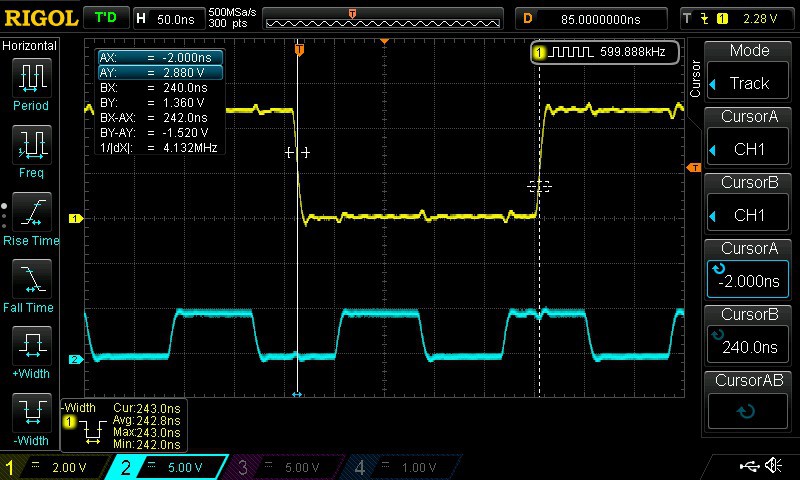
When I ran the code the oscilloscope connected to the Output Enable line of the SRAM showed that there were three accesses to addresses 0, 1 and 2 which is what I expected.
MREQ* (top) and CPUCLK (bottom). Looks good.
![]()
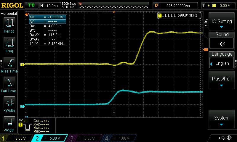
Propagation delay from the PSoC logic. MREQ* on the bottom, SRAMOE* on the top. Less than 20 nS. Comparable to LSTTL speeds "in the day".
![]()
So far, so good.
Next task is getting some I/O emulation running.
Perhaps start with a single 1-bit register connected to an LED? Need some Output to I/O space code to make that work.
-
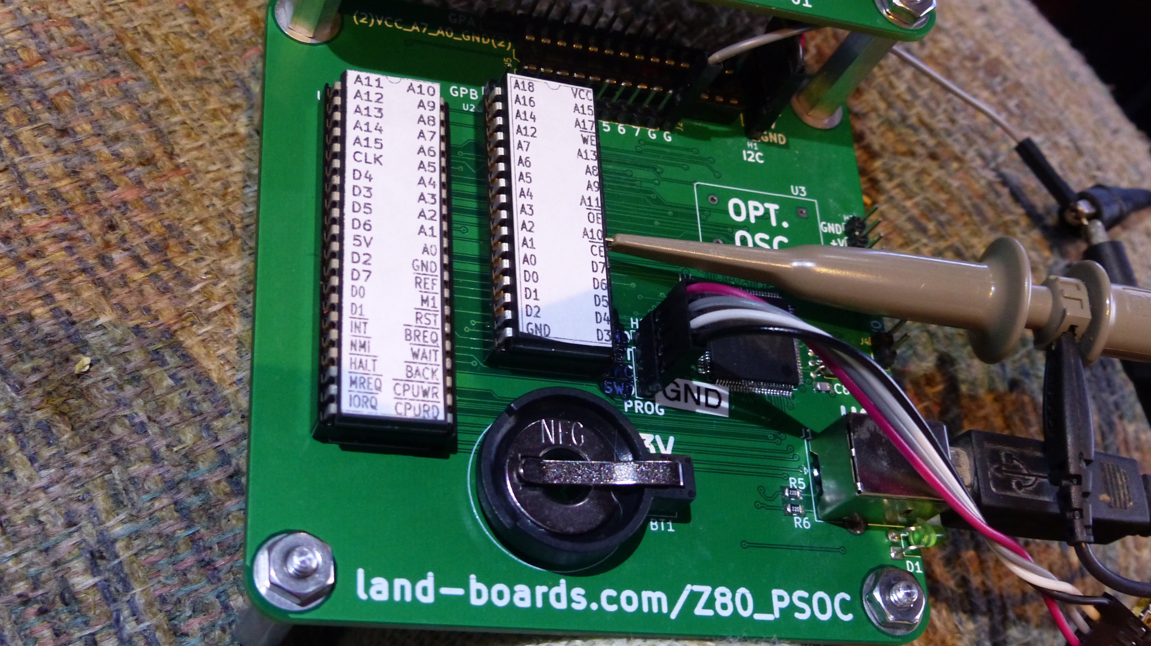
Z80 and SRAM Labels
10/10/2019 at 01:07 • 0 commentsWe added labels for the pins on the Z80 chip. The labels make is easier to probe around with an oscilloscope to look at pins.
![]()
We made the stickers from the KiCad PCB layout tool. They were printed on label paper at 1:1 accurate scale. The character height was around 0.06" which spaces them correctly for the part.
The next rev of the board with have the pins in silkscreen.
![]()
3-Chip Z80 Design
Combining a Z80 retro design with a modern PSoC CPU.