land-boards.com
-
Z80 PIO Emulation
09/25/2019 at 19:08 • 0 commentsThe Z80 PIO has two 8-bit ports. This can be emulated (albeit slower) with the MCP23017 I2C port expander and the PSoC. If speed doesn't matter, then the MCP23017 should work just fine.
The Z80 views the I/O space as if a real PIO chip was present. Just like the example previously for the Serial IO chip the PSoC sees the request to access the PIO and translates the request to I2C transfers to the MCP23017. Bits can be set as input or output and read or written as needed.
I've added an optional MCP23017 to the card to support this PIO emulation. The chip is hardwired on the card to address 0x20. It should be socketed in case larger external I/O requirements are needed.
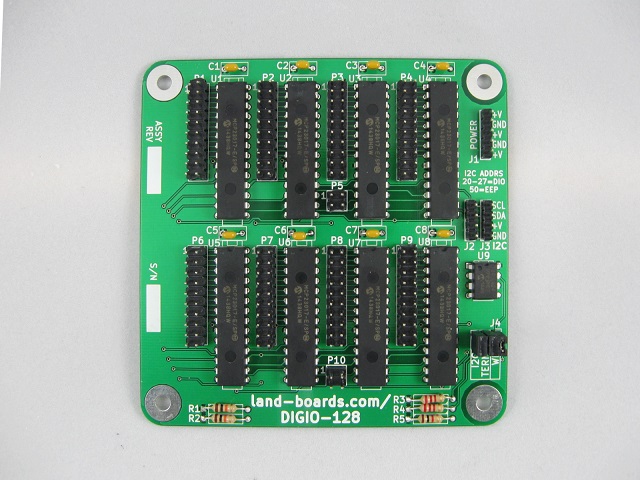
I've designed a bunch of I2C cards. One card, the DIGIO-128 even has 128-bits of I2C space but it uses the entire 0x20-0x27 address space. These cards are ODAS form factor like this CPU card (95x95mm).
Here's the DIGIO-128 card for reference.
![]()
-
Retro-future Front Panel
09/25/2019 at 16:28 • 0 commentsSince the 3-Chip Z80 allows the PSoC to load the SRAM and control the Z80 it would be fun to imagine how a front panel would work. Something like one of those very classic front panels with switches and LEDs on it. But re-imagined for the present.
What I don't care for about the original front panels is the expensive rocker switches. They look retro-cool, but cost a lot of money. For this design, I'm going with clicky pushbutton switches and using software on the PSoC along with the LEDs on the board to treat the switches as if they were toggle switches. Push a button and the corresponding LED toggles on or off.
For this we need 16 address, 8 data and some number of control switches/LEDs.
Hardware
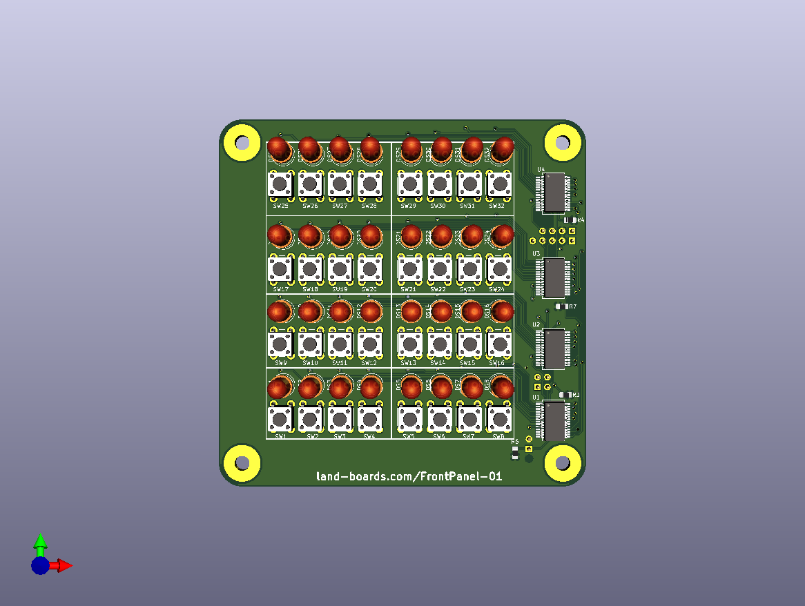
The PSoC has an I2C bus. I've designed an I2C card with 4 of MCP23017 16-bit port expanders. Each of the port expanders has 16 bits of I/O. Here's what I came up with for a PCB design.
![]()
There are four rows of 8 switches and 8 LEDs. Each switch and led is connected to individual lines into the MPC2017 chips. These take up 4 I2C addresses - either 0x20-0x23 or 0x24-0x27. The I2C A2 address value is selectable via jumper.
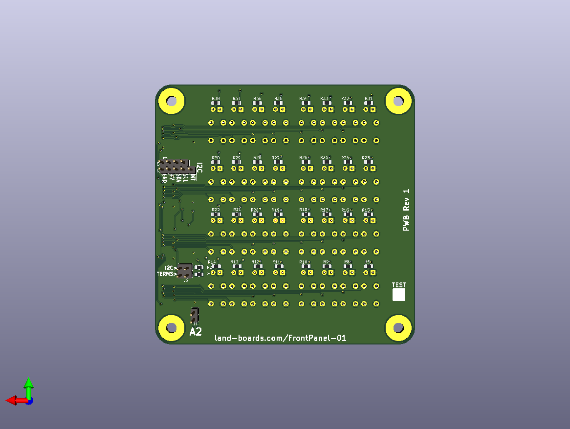
The I2C bus uses SDA and SCL plus Power/Ground. There's an interrupt from the card for change of input states which is programmable in the MCP23017. There's a daisy-chain connector to allow other I2C devices to be chained off the first device. There are jumper selectable terminators on the card as well. These are all accessible from the rear of the card.
![]()
The card could be stacked with the 3-Chip Z80 card and wiring brought from the I2C interface on the top side of the Z80 card up to the back of this card. The two cards have the same ODAS 95x95mm design with 6-32 mounting holes in the same spots for stacking with stand-off hardware.
Software
The Software to talk to the Front Panel is all contained inside the PSoC. The software detects key presses and sets LEDs accordingly.
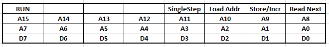
A notional button/LED setup is something like this:
![]()
When an interrupt is received the PSoC goes to the I2C bus and determines which bit was changed. The PSoC is responsible for key debouncing which it can do by reading the buttons several times. Pressing D0 for instance, will toggle the value of the D0 LED.
The top row of buttons tell the PSoC to do operations like:
- Run the program from the address on the address LEDs (A15..A0)
- Single step the program from the address on the address LEDs
- Load Addr lets the address that is currently be selected load from memory
- Store increment stores the value that is currently on the data LEDs to the SRAM
- Read Next advances to the next read address in the SRAM and reads the current value (without storing)
This requires a small change to the PSoC design to add an interrupt line from the I2C header. I also added an optional MCP23017 to the PSoC card to all for PIO chip emulation and provide general I/O.
-
Current Resources - Work Left to Do
09/24/2019 at 01:24 • 0 commentsWhat is done?
- I/O space design is designed
- Memory space design is designed
- USB, I2C and Serial port peripherals are included
The resources of this consume about half of the programmable logic in the PSoC.
![]()
Still to do
- Add two address bits for SRAMA[12..11]. This is an enhancement out of the memory mapper implementation and allows for minimum 2KB block size mapping.
- Interrupt controller - generate interrupts to the Z80. That should be as simple as the PSoC setting the NT* line to the Z80 and the bit would be cleared by an interrupt acknowledge cycle from the Z80.
- It would be fun to add connections to the DAC for sound generation. This could be controlled by the PWM in the PSoC.
I am not yet I/O limited but getting there soon. I could free up the BREQ* and BG* lines since I'm not planning on using that functionality.
-
Loading SRAM Initial Contents
09/24/2019 at 01:06 • 0 commentsLoading the initial SRAM contents falls out of the previous design considerations with a couple of minor additions to control logic.
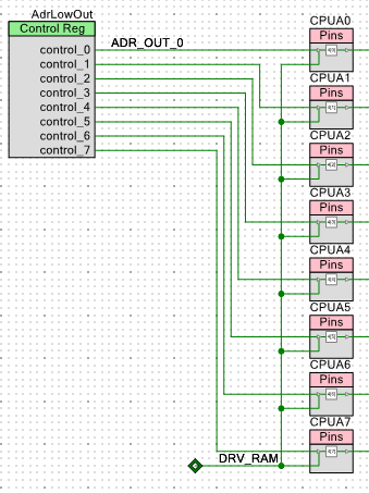
SRAM address lines A0-A7 are handled as follows:
![]()
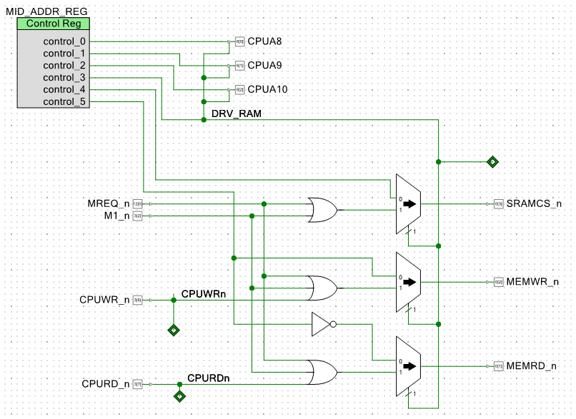
An 8-bit control register contains address bits 0..7. The next section of logic creates address bits 8..10 and the DRV_RAM signal which drives the address lines onto the address bus of the Z80. The Z80 must have surrendered the bus via either:
- Being held in reset by the PSoC
- Bus surrendered by the PSoC asserting BREQ* (Bus Request( and granted by the Z80 asserting BGR* (Bus Grant).
The first method is the most obvious since the CPU won't run until a program is loaded into it.
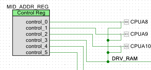
Address lines 8..10 are controlled as follows:
![]()
These mid range addresses as well as the DRV_RAM control signals are all output from the PSoC MID_ADDR_REG register.
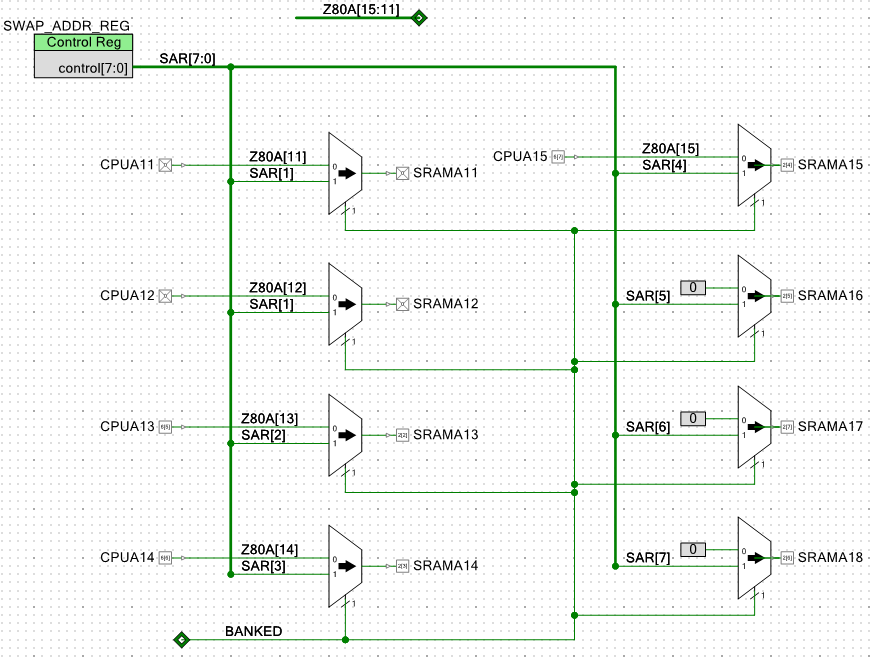
The upper address lines fall out of the memory mapper described in the previous log post.
![]()
The SRAMA11..18 lines are the value of the SWAP_ADDR_REG. They don't need to be trisstated since they only go to the SRAM. There needs to be an additional factor in the BANKED signal, namely the DRV_ADR which should force the multiplexers to always use the SWAP_ADDR_REG as the source of address during loads of SRAM. DRV_ADR is added to the comparator output as follows:
![]()
Control Logic
The control logic for loading SRAM is conventional and fairly uncomplicated. It is contained in the same register that controls the mid addresses (above). It looks like:
![]()
There are 2 output bits. One is Read/Write which controls the MEMWR* and MEMRD* and the other strobes the SRAMCS*.
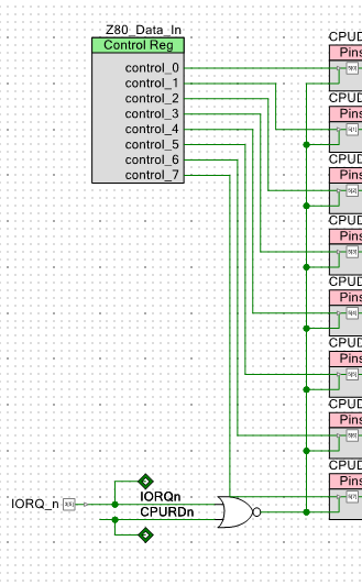
Data Bus
There is a register (the Z80_Data_In register) which puts data out on the Z80 data bus. It's already used for I/O reads from the Z80. This same register can be used to put data into the SRAM.
![]()
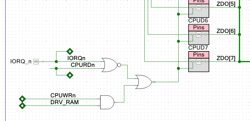
The control signals need to include the DRV_RAM signal and the MEMWR* control lines. Here's that added logic:
![]()
That should be all that is required to load the program into the SRAM.
-
Z80 Memory Mapping/Bank Switching
09/23/2019 at 18:16 • 1 commentBank Switching is used for RAM Disks and possibly other applications where more memory than the CPU address space is desired.
There are quite a few Z80 memory bank switching schemes out in the wild. Many of them complicate things by trying to replicate a Memory Management unit with multiple banks that can map into multiple locations. For a typical discussion of where this can go see this EEVBLOG thread which goes on for many pages.
Control of bank switching can be done with the PSoC and the Z80. Changing to another bank typically consists of an I/O write from the Z80 to a bank select register. This switches the address of the bank. The PSoC just sees the memory bank control register as a single [up to] 8-bit I/O write which replaces the upper address bits to the SRAM when accesses are in the range of the window.
In the simplest scheme, bank switching involves creating a single window in the Z80 memory space and switching in banks of SRAM into the window.
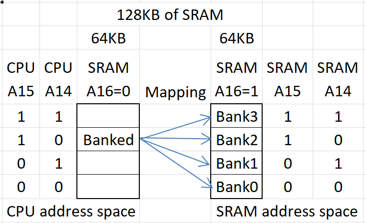
This is an illustration of the concept for a 16-bit address bus CPU (like the Z80) with a 16KB bank size and a total of 128 KB of SRAM.
![]()
In the example, if the CPU Address is 0x8000-0xBFFF, the bank switch is selected. The upper SRAM address, A16 gets set to 1. Any other CPU address does not get translated but gets directly sent to the SRAM and A16=0. The "Banked" area is actually not filled in the "original" SRAM. SRAM address lines A16..A14 come out of the mapper but only when the CPU address range is the banked space. Outside of the banked range the address lines are unchanged.
The complicating factor here is that the Z80 bank addresses A15 and A14 are replaced by the bits from the bank select register but only when the address is in the banked window. This is set by the Z80 CPU with an I/O write. The relevant factors for banking are:
- Size of the SRAM
- Size of the window
- Address range of the window
The size of the SRAM determines how many banks there will be. The window size determines how many of the upper address bits are altered. The range defines where that mapping happens from the Z80 CPU side and how many bits have to be sent out to the SRAM.
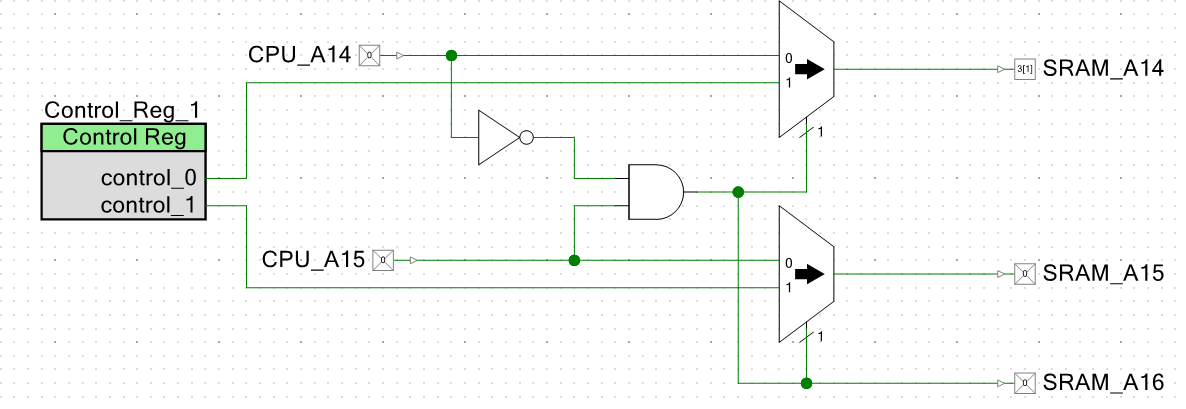
This simple map is implemented as follows:
![]()
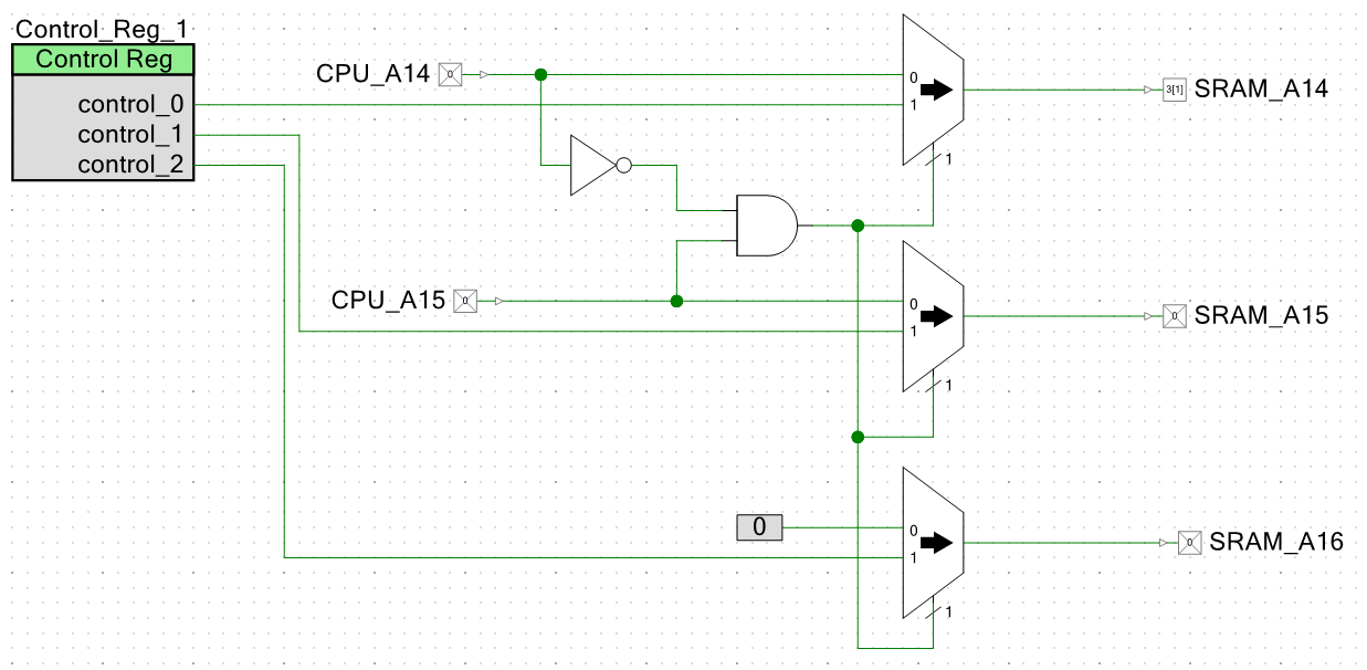
To generalize, SRAM_A16 could be handled with an extra bit from the Control_Register_1 and an additional multiplexer. With this method the 16KB that was "lost" could be recovered. But the mapping register contents have to be more carefully considered to not cause a conflict with the base page. In this instance, it means that the A16 should always be set to 1. Ranges outside of the bank select 0 for SRAM_A16.
![]()
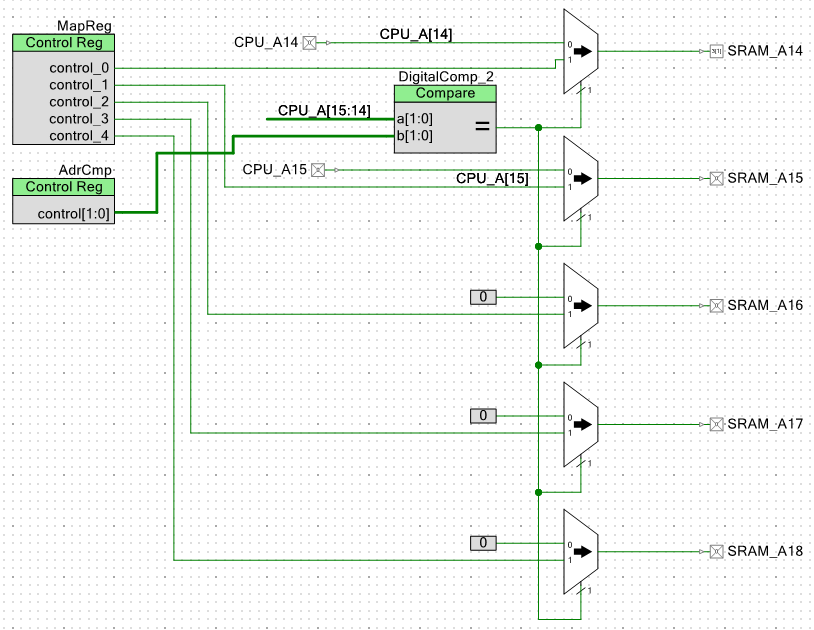
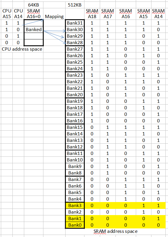
Replacing the SRAM with a larger part, say a 512MB part which has 19 address bits, requires adding two extra SRAM address bits A17..A18. The map register needs 5 bits A14..A18. Address SRAM_A16 also needs to also be treated differently. If the bank size is the same, there's no difference in the A14=0, A15=1 decoding. Also, replacing the NOT-AND gate with a comparator against a value from a register allows any 16KB range in the CPU address space to be replaced by the Banked address.
![]()
However, this method introduces a problem, namely banks 0, 1, and 3 now overlap the original unbanked memory space.
![]()
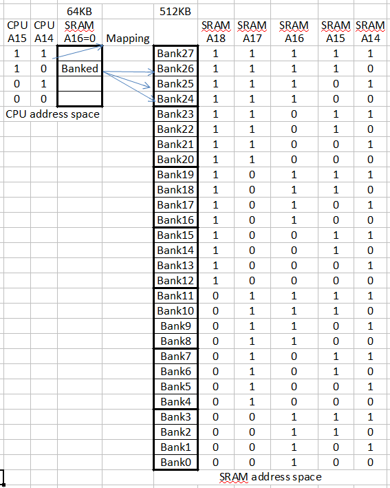
There are two solutions to this problem. Either the Z80 can never ask for overlapping regions, or the PSoC can add 64K to the bank address register to avoid the bottom 64KB. The later is the easier solution. For 512KB of SRAM and 16KB banks, this reduces the number of banks from 32 to 28 but 3 of those banks should not be used anyway. Losing the extra bank (Bank 2 in the illustration) is not much of a hit (1 bank out of 28/32 isn't a big deal). The Z80 could not ask for any banks above 27.
This would be:
![]()
This addition of 4 to the passed bank register value could be done with adder hardware in the mapper or by the PSoC when the bank register value is handled by the PSoC. The later is the easier.
Generalizing the design
As shown, this can be done with fairly straightforward logic but it's a bit harder to generalize the design. Generalizing involves masks and "variable" comparators. At the conceptual level, the mask sets the number of address bits and the comparator looks to see if the Z80 is in the banked range. The two are related. Only bits which are not mapped get compared. Ideally, it would be nice to have both the size and start of the range be programmable. Then, it only needs to be designed once. The PSoC would set this general purpose to make the software needs.
From the perspective of the PSoC, a convenient bank control register size is 8-bits. This would cover SRAMA[18..11]. This means address lines CPUA[10..0] are untranslated. This is a 2K minimum size for the swap block. For 512KB this means there are 256 blocks (the 8-bits of the bank control register). Block sizes need to be a power of 2 and are design/software specific so it would be good for the PSoC to be able to set them under program control depending on the software build.
The CPU address comparator needs to look at A15..A11. This is 5-bits. Any address that does not match these compare bits would get passed through unchanged. But it is desirable to have bank size configurable as well since different builds could use 2K, 4K, 8K, 16K or 32K swap ranges. This necessitates a 5-bit mask register to select the bits that are compared.
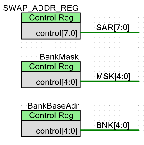
These control registers are like this:
![]()
SWAP_ADDR_REG originate from the Z80 CPU plus the offset necessary to avoid the first 64KB. This means that A16=1 is always added to the value. The Z80 ultimately controls whether or not swapping happens by addressing memory in the banked range. The Z80 also determine which SRAM bank gets swapped in by the value it writes to the SWAP_ADDR_REG. The PSoC protects the unbanked space by never allowing writes to the first 64KB of SRAM (adding in the plus 4 into the SWAP_ADDR_REG from earlier).
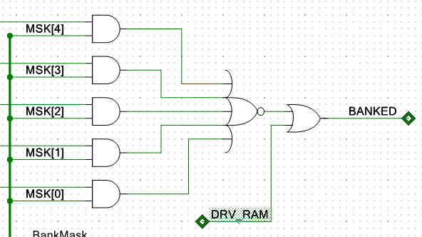
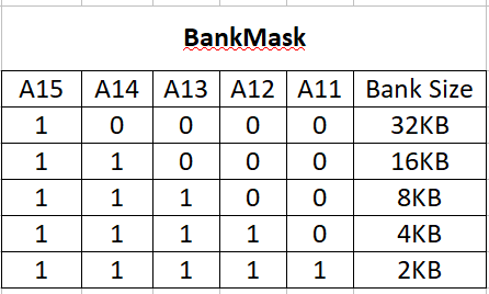
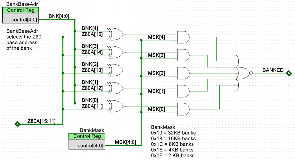
The BankMask is set by the PSoC. It determines the bank size and should be known for a given software build from the memory map of the software. Bank sizes are 2K, 4K, 8K, 16K and 32K so this could be implemented with a 3-bit register and a thermometer decoder. It is easier to set the values directly. Values are:
![]()
Writing 0x10 to the BankMask selects 32KB banks. Writing 0x1F to the BankMask selects 2KB banks. This is implemented in C as:
#define SRAMBANK32KB 0x10
#define SRAMBANK16KB 0x18
#define SRAMBANK8KB 0x1c
#define SRAMBANK4KB 0x1e
#define SRAMBANK2KB 0x1f
The BankBaseAdr is the address range that is used for comparison with the Z80 CPU address bits. It is masked by the BankMask which determines the number of bits which should be used. It is a constant value and is also known for a given builds.
With this information we can build the bank address range comparator.
![]()
The XOR does a comparison of the BankBaseAdr bit with the Z80 Address. If the bit is different the output of the XOR is 1. The BankMask bits determine whether or not the bit "matters" in the comparison. The output is the BANKED signal which indicates that the selection is banked.
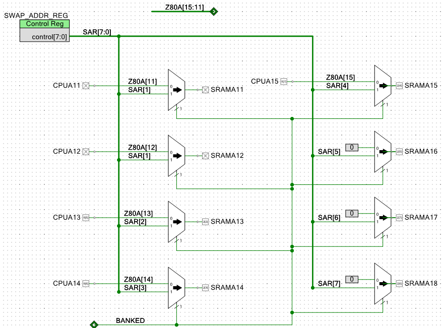
The Address mapping, then, is performed with a set of 2:1 multiplexers. The BANKED bit controls the multiplexer selection.
![]()
So the only caveat here is that the bank select register has 4 added to it before it is put into the SWAP_ADR_REG. This would not be necessary if the Z80 software is aware of the banking scheme.
-
Z80 Serial IO (SIO) Emulation - Worked Example
09/23/2019 at 17:30 • 0 commentsSerial I/O Emulation
Normally, serial I/O using the 6850, SIO or DART consists of two I/O mapped locations per serial port. One I/O address is for data read/write. The other I/O address is for status/control. In the case of the 6850 UART this reduces down to just two bits of status (Transmitter full and Receiver empty) and the 8-bit data read/write register.
Polled Serial I/O
Serial output from Z80 works by the Z80 polling the Transmit not full register waiting for transmit not full and then writing the data to transmit in the Transmit Output buffer. This action is emulated by the PSoC. The Z80 requests the status register value which the PSoC presents. The PSoC determines the value that should be sent to the status register by looking at it's own UART interface. If the PSoC UART transmitter is not full then it returns that status to the Z80. The Z80 sees that the transmitter is not full and then sends out the transmit byte. The PSoC picks up the transmit byte and puts it out to the UART.
Read operations are similar. The Z80 reads the UART status register which is emulated by the PSoC and waits for receive data to be present. It then requests the data by performing a read which causes the PSoC to read the UART and return the value to the Z80.
From the PSoC Perspective
From the PSoC operations consist of either waiting for an interrupt or polling the IO_Stat_Reg and waiting for IORQ* to go active.
When IORQ* goes active the PSoC then takes the values in the IO_Stat_Reg status register to determine the operation. It also takes the address from the AdrLowIn status register to determine the peripheral address that is being accessed by the Z80.
Interrupt Driven I/O
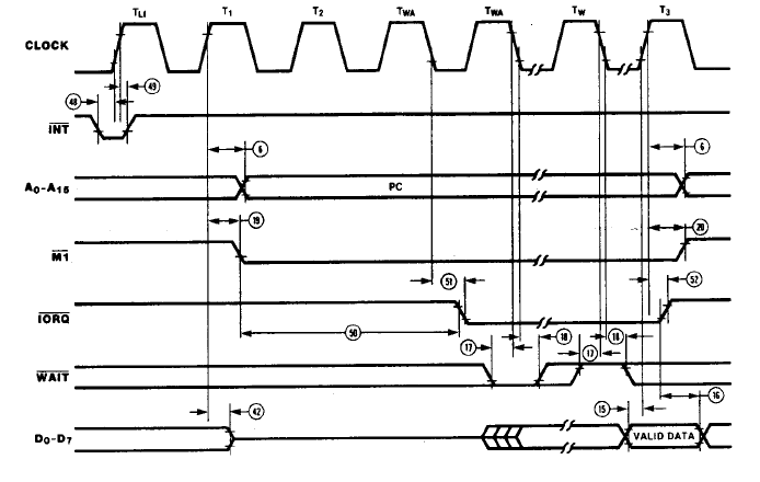
Interrupt driven I/O is only a bit more complicated. The PSoC generates the INT* line to the Z80 indicating that an interrupt is present. This causes the Z80 to issue the following timing:
![]()
In response, the PSoC places the interrupt vector onto the data bus to the Z80. This operation by the Z80 is similar to an I/O read with the exception that the M1* line is active (low) during the read of the interrupt vector. The PSoC sees the M1* line low and knows that this an I/O operation reading an interrupt vector.
This behavior can be emulated by the PSoC by monitoring the M1* line.
![]()
The PSoC sees the M1* line low and knows that this an I/O operation reading an interrupt vector. This seems to be a common source of confusion for many designers who do not include M1* in their logic. If it's a standard Z80 peripheral chip it probably knows to not send out normal data, but send out the interrupt vector.
The interrupt vector could be implemented with some additional logic in the PSoC but would come at the cost of 8 of 2:1 multiplexers on the data bus out of the PSoC to the Z80. With this emulation method there's no real advantage to adding extra logic for this function. If M1* is high then the read is a "normal" I/O read. If the M1* is low then the read is an interrupt vector read. In either case, the PSoC provides the requested value.
The reading of the interrupt vector by the Z80 is the interrupt acknowledge and will remove the interrupt.
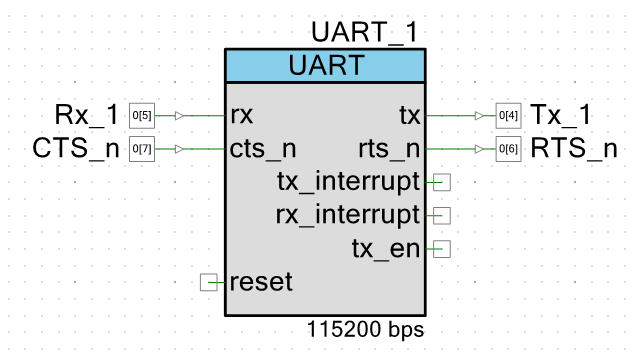
The PSoC hardware to implement the external UART is relatively straightforward.
![]()
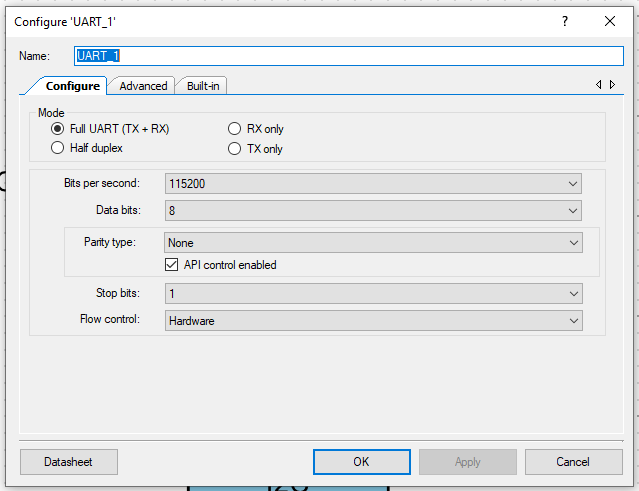
The Configuration for the UART is:
![]()
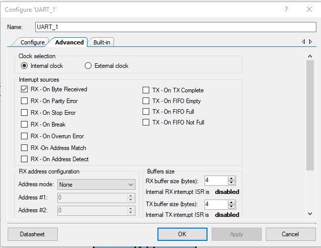
This configuration allows the UART to be software controlled (for baud rate and other configuration values). It also provides hardware handshake lines. The PSoC UART can be set up to interrupt on various conditions.
![]()
These can be used to mimic the interrupt characteristics of the Serial I/O being emulated.
Sequence of Operations - Serial In - Polled
The steps to receive data from the serial port are:
- Z80 issues a read request to the UART Status register address
- PSoC receives the read request either by polling the IO_Stat_Reg or by receiving an interrupt via IO_Op_Int
- PSoC reads the I/O address from the Z80 - by reading AdrLowIn status register
- PSoC classifies the transfer as a normal read of I/O at the status address loaded from AdrLowIn
- PSoC figures out the receive status by checking the receive character status by calling the function auto-generated by the PSoC Creator (essentially an application builder) called UART_1_ReadRxStatus( )
- PSoC similarly figures out the transmit status by calling UART_1_ReadTxStatus( )
- The PSoC packs the responses into a return value and puts the value into the output mailbox Z80_Data_In
- The PSoC indicates to the Z80 that the status data has been read by pulsing CLR_IO_INT
- The Z80 repeats these above steps until there is a receive character
- The PSoC doesn't know why the Z80 is requesting status (it could be for a transmit or receive) so it needs to pack all of the bits into the status everytime
- After the Z80 sees that the data is present, it sends the Serial IO data register address to the PSoC
- The PSoC reads its UART and returns the data (as above for status)
Sequence of Operations - Serial Out - Polled
This is very similar to the above example for reads. The difference is the transmit bits are used.
This all seems complicated but it's really not all that complicated. Basically, the function of the I/O interface of any Z80 peripheral can be emulated by the PSoC. This consists of emulating the internal registers of the peripheral and connecting them to the peripheral functions in the PSoC. The UART example above is familiar. Others may be less familiar. Some, like timers may require additional sofware/hardware in the PSoC to emulate the function of the chip.
The beauty of this design method is that the peripherals can be switched in/out of the design by creating a bit of code to emulate their control/status interface and the PSoC can do all of the work.
-
Z80 I/O Emulation - Hardware
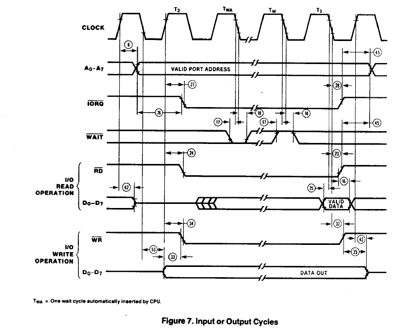
09/23/2019 at 15:19 • 0 commentsZ80 I/O peripherals can be emulated by the PSoC. The Z80 I/O timing is:
![]()
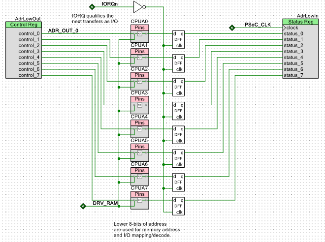
The Z80 address bus is stable 107 nS min (26) prior to IORQ* falling edge which provides the setup time for the address register. PSoC AdrLowIn status register is the Z80 latched address which is read by the PSoC. The register is latched with the falling edge of IORQ*.
![]()
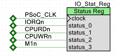
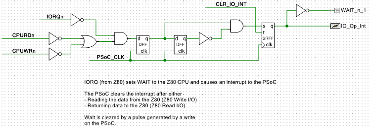
The PSoC reads the AdrLowIn status register and determines which peripheral needs to be emulated based on the address. This operation is gated by an interrupt generated when IORQ* and (CPURD* or CPUWR*) are present. This looks like:
![]()
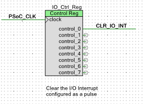
The qualified I/O transfer sets the RS Flip-Flop for the interrupt to the PSoC and automatically causes the WAIT* to be asserted to the Z80. This is cleared by a write to the IO_Ctrl_Reg which is configured to generate a pulse when the CLR_IO_INT bit is written.
![]()
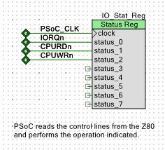
The PSoC reads the IO_Stat_Reg to determine the operation that the Z80 requests with the IO_Stat_Reg.
![]()
Data Mailboxes
There are two 8-bit mailboxes. There is a send mailbox (to Z80 from perspective of the PSoC) There is also a receive mailbox (from Z80 from the perspective of the PSoC).
Summary
Sequence works like this:
- Z80 asserts IORQ*
- Falling edge of IORQ* latches the Z80 address into the D Flip-Flops
- Z80 asserts CPURD* or CPUWR*
- The assertion of IORQ* and CPURD* or CPUWR* sets the R-S Flip Flop which asserts IO_Op_Int (interrupt to PSoC) and asserts WAIT* to Z80
- The PSoC reads IO_Stat_Reg to determine the Read/Write direction
- The PSoC reads the lower address bits from the Z80 from the AdrLowIn status register
- PSoC determines the peripheral action from the address and CPURD* or CPUWR* lines
- The peripheral action can be performed by looking up the address and read write in a C function pointer table or with if-else code (depending on the number of peripherals being emulated
- If the operation is a write, the data is read from the Z80_Data_Out status register
- If the operation is a read, the data is placed into the Z80_Data_In control register
- The transfer is acknowledged by writing to the CLR_IO_IN register
-
PSoC Logic Resources
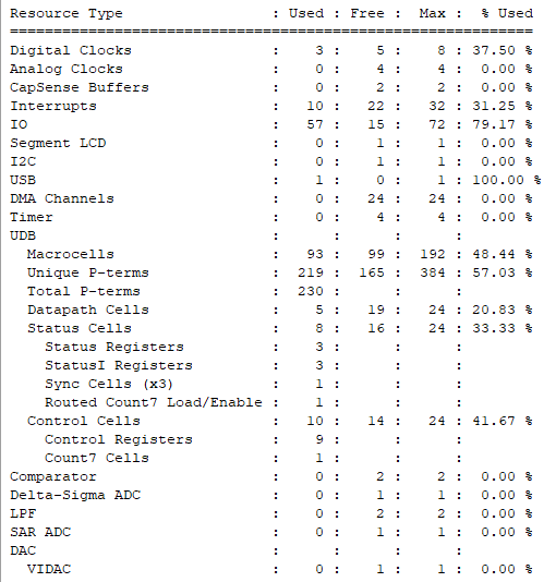
09/22/2019 at 14:35 • 0 commentsI've done quite a few PSoC designs. Some of them have reached the limit of logic that can be placed into the Programmable Logic area of the PSoC. The question is how many peripherals can be emulated in the PSoC before resources run out.
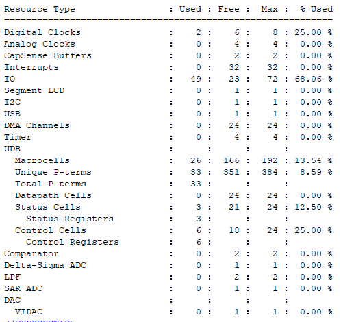
Currently I've got a UART emulator in the design. It has a status register and control register that can be read/written from the Z80. It also has data registers in both directions. The current resource planner shows that only 26 / 166 (about 14%) of the macrocells are being used.:
![]()
6 of the 24 Control Registers and 3 of the Status Registers are used.
This leaves plenty of logic to implement functions directly as well as more Control/Status registers to emulate the Peripheral ICs.
-
Performance
09/22/2019 at 13:43 • 0 commentsThe performance should closely match the original designs.
CPU Performance
The program memory needs to be able to keep up with the CPU. The CPU should be able to run with no wait states. Let's verify the timing works.
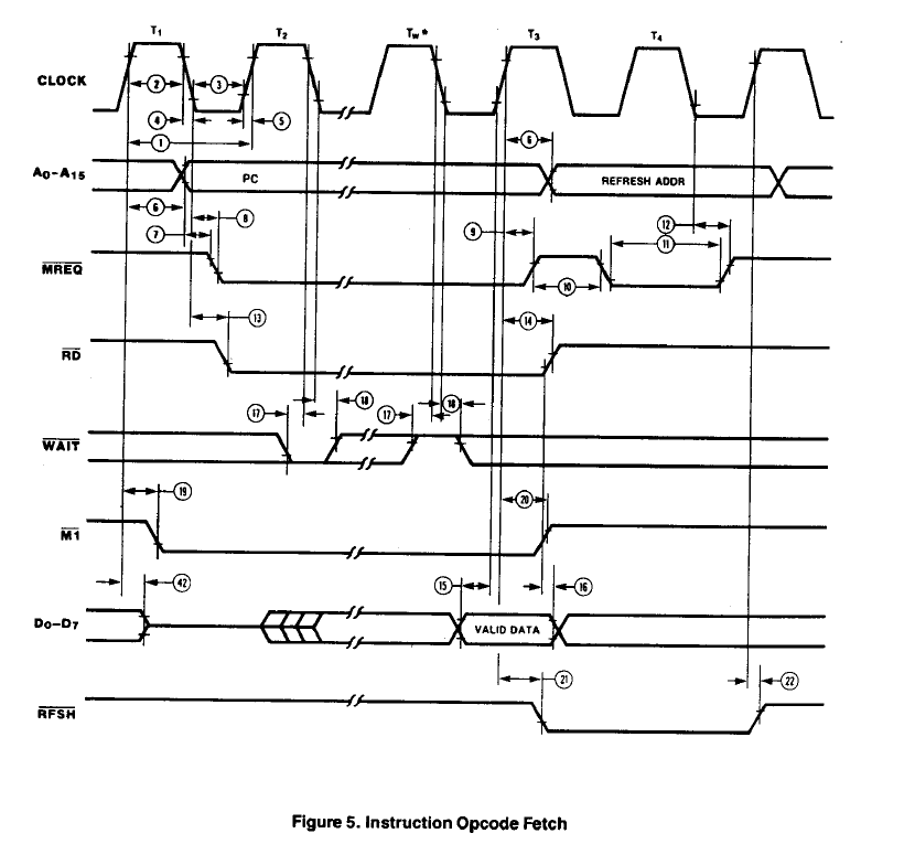
Opcode Fetches
Opcode fetches take four clocks on the Z80 (plus any wait states). The CPU is run at 8 MHz (could easily be pretty much any available speed) The RD* strobe is approx 1-1/2 clocks wide. With a 6 MHz CPU (166 nS clock rate) this is 249 nS. MREQ* drops 80 nS max (13) after the clock falling edge. Data is read on the rising edge of T3 and has a required setup time of 30 nS min (15). The address is guaranteed to be valid 35 nS before MREQ* falls.
The SRAM access speed is specified from address being valid. The address is valid 90 nS max (6) from the rising edge of T1. It is also guaranteed to be valid prior to MREQ* falling by 35 nS (min).
Timing would then be the 249 nS minus 80 minus 30. If the SRAM is faster than 139 nS it will run with no wait states. The SRAM I selected is 55 nS so it is more than fast enough to read instructions without wait states.
![]()
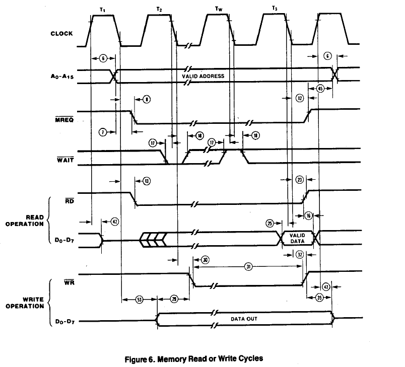
Data Reads/Writes from/to SRAM
Data read timing is identical to opcode read timing so there's no issue for speed. Writes are set by the width of the WR* pulse. This is 132 nS (31). This also is fast enough. Fortunately the data hold time after RD* rise is 0 nS (16).
![]()
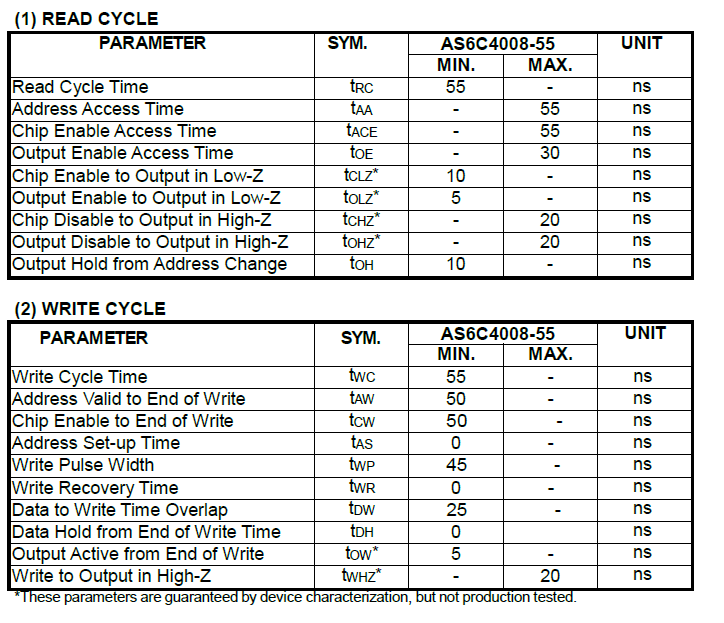
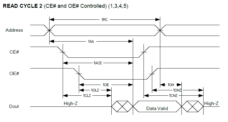
SRAM Timing
The SRAM timing shows that the output enable to output is very quick.
![]()
Read Cycle timing is:
![]()
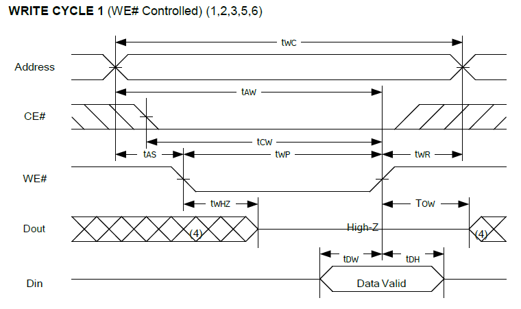
Write cycle timing is:
![]()
I/O Performance
The only speed exception could possibly be reading of peripheral devices (and writing of some devices). That is because the devices are essentially emulated by the PSoC. I/O may need to assert wait states.
![]()
-
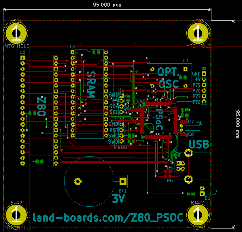
Updates layout and 3D
09/22/2019 at 13:40 • 0 commentsAdded H3 for Serial or SPI or other I/O. I had to do a lot of pin shuffling on the PSoC to make the routing possible in 2 layers.
![]()
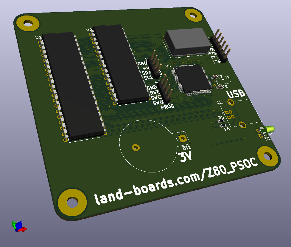
3D view
![]()
3-Chip Z80 Design
Combining a Z80 retro design with a modern PSoC CPU.