-
Switches and debouncing
12/03/2019 at 16:20 • 0 commentsNow that that first version of my CPU is running, it is time to fix some issues. One of them is manual switches and debouncing.
I will not write one more article about debouncing as all this is very well detailed in the great article by Elliot Williams Debounce your noisy buttons.
In this first version of my CPU I ended up with the following switches
- Bus Publish : This pushbutton published the value of a dip switch to the bus
- Master Reset : This pushbuttons resets the computer
- Memory manual Write : This pushbutton writes the data set on the data dip switch at the memory address set on the address dip switch [PRO mode only]
- PROG/BUS selector : this is a two way selector used to program the memory (PROG mode) or to use the memory through the regular bus and Memory Address Register (BUS mode)
- MANUAL / AUTO clock selector : this is a two way selector used to select between the automatic clock (slow or fast) or the manual pulse pushbutton
- SLOW / FAST clock selector : this is a two way selector to swicth between the 555 base slow clock (between 0,5Hz and 300 Hz) and the fast cristal oscillator based clock (1 Mhz) [valid for Auto clock mode only]
- MANUAL / AUTO uCode selector : this is a two way selector disabling the microcode decoder in order to use manual action signals (debugging purposes only)
3 are pushbuttons and 4 are two way selectors (slide buttons).
In is articule, Elliot explains how to debounce using an RC (Resistor/Capacitor) circuit and a schmitt trigger inverter. The inverter can be found in the 74HCT14 IC.
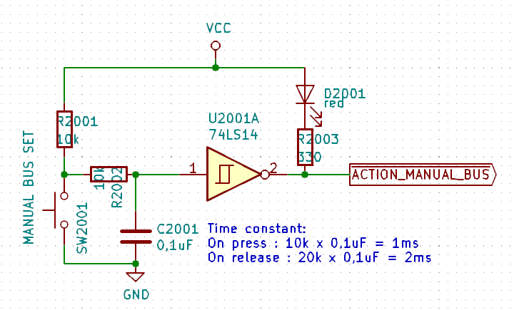
Here is an example of a complete debouncer. Note that the signal is inverted : when pressing the button, the signal ACTION_MANUAL_BUS goes low.
Here a short description of how it works :
When the switch is open, the capacitor is loaded through the 10k + 10k resistors and reaches VCC. The output signal is then 0V (inverted input)
When the swicth is pressed, the capacitor is unloaded through the 10k resistor, it will therefore take 1 ms to reach 1/3 VCC and trigger the change of state of the inverter
When the switch is released, the capacitor is loaded again, it will reach 2/3 VCC in 2ms and trigger the change of state of the inverter.
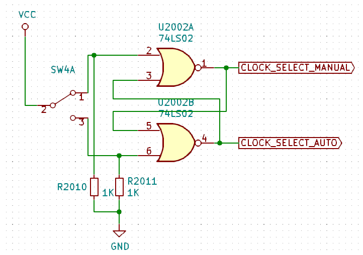
For the slide swicthes (type is break before make), we need to prevent any oscilation between the two states and prevent an unknown state. The best solution here is a simple SR latch.
An SR latch (in this cas an SR NOT latch as it is built using 2 NOR gates) can only be in 1 of 2 states.
When moving the switch from on position to the other, what may happen is the following:
- bounce off the first state
- stay undefined (in between the two states)
- bounce on the second state
In such a situation, the SR latch will prevent any oscillation following the reasoning:
- When the switch bounces off, the latch will stay in the same status (set or reset)
- when the swicth is undefined, the latch will stay at the same status
- the first time the witch touches the other positon the latch will toggle but even if the switch bounces it will stay in that second position.
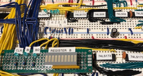
So in the end, I have built a dedicated breadboard with all the swicthes, RC circuits and IC to debounce all and have perfectly clean manual signals.
-
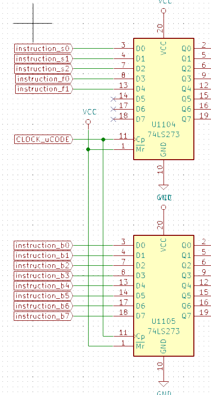
The need for a decoder register
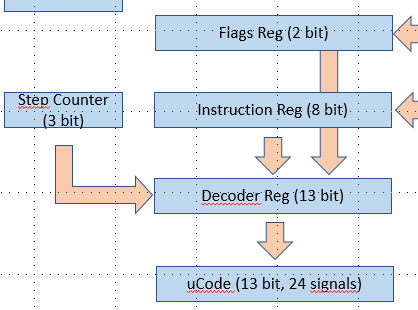
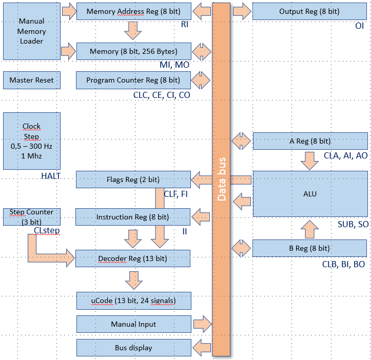
11/20/2019 at 15:27 • 0 commentsThe decoder section of the architecture diagram shows a 13-bit decoder register.:
What is the rationale behind the need for this register?
In order to properly set the action signals, there is a need for 13 bits to address de EEPROM used to implement the micro-code:
- 3 bits for the steps (count from 0 to 7 steps maximum, however most macro-instructions will only need 3 or 4 steps)
- 8 bits for the instructions (not all 256 capabilities will be used)
- 2 bits for a combination based on the flags register
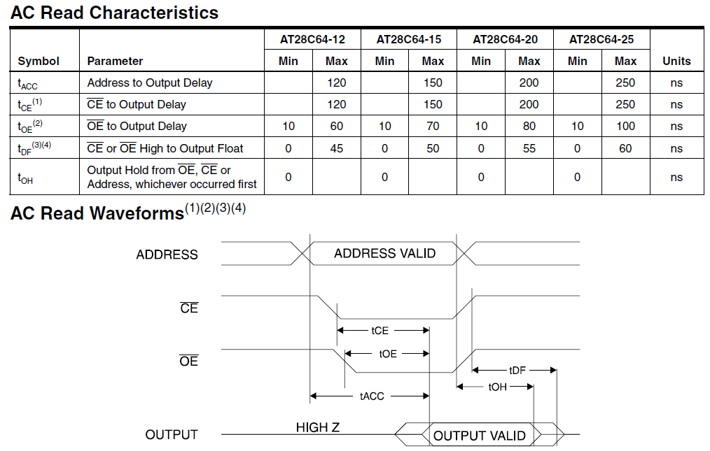
However, when looking at the specs of the EEPROM (AT28C64) we can see that in the worst case, between the stabilization of the address inputs and the availability of proper stable output it can take up to 250ns. This means that if bits from the address are not stable the output might not be valid.
This is why the implementation of a register used to create a stable snapshot of the 13 bits will help providing stable action signals.
This is actually a perfect use case for the 74HCT273 register we already talked about. What we need is the capability to snapshot tu status of the 3 elements (register, steps, flags) at a given time and keep it stable until the next clock cycle:
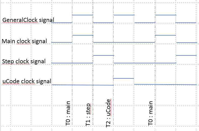
Now the question is : when are values changed (step, instruction register, flags)? When in the overall instruction cycle are they stable enough that I can snapshot them ?
Well if we look at the clock cycle we can identify 3 moments:
- main clock (rising edge) : when the actions take place (add, load, etc)
- step clock : when the step is incremented
- uCode clock : when to hold the value of the 3 elements that constitute the micro-instruction register
So we need 3 clock rising edges per step cycle:
If the main clock signal is at 1Mhz, we get 1ms between general clock rising edges. So that is:
- 500ns between T0 and T1
- 500ns between T1 and T2
- 1000ns between T2 and the next T0 which is more than enough to stabilize the EEPROM values
-
Micro Instructions
11/19/2019 at 10:22 • 0 commentsAll the initial modules are now built, it is time to document the list of Micro Instructions.
Here is a map of all the available Micro Instructions assigned to each modules:
[unless specified, all actions are synchronous on the CLOCK_MAIN clock signal]
A register
- CLA : Clear A : reset value to 0 - Asynchronous
- AI : A register In : Load A register value from bus
- AO : A register Out : publish A register value to bus
B register
- CLB : Clear B : reset value to 0 - Asynchronous
- BI : B register In : Load B regisister ter value from bus
- BO : B register Out : publish B register value to bus
ALU & Flags
- CLF : Clear Flags : reset flags value to 0 - Asynchronous
- SUB : Substract function : apply substract function (default is Add)
- SO : ALU Out : pubish ALU result value to bus
- FI : Flags In : set flags based on current value of ALU output
Instruction register
- II : Instruction In : Load instruction register value from bus
Step counter
- CLstep : Clear Steap : reset counter to 0 - synchronous on CLOCK_STEP clock signal
Clock
- HALT : stops the clock
Program counter
- CLC : Clear Program Counter : reset Program Counter value to 0 - Asynchronous
- CE : Program Counter enable : increment Program Counter value by 1
- CI : Program Counter In : load Programl Counter value from bus
- CO : Program Counter Out : publish Program Counter value to bus
Memory Address Register
- RI : Memory Address Register In : load Memory Address Register value from bus
Memory
- MI : Memory In : Load value from bus and store it in memory at the address specified by the Memory Address Register
- MO : Memory Out : publish value of memory at address defined by the Memory Address Register to the bus
Output Register
- OI : Output In : load Output register value from bus
Some of these signals will be connected to the Instruction Decoder, some are connected to the reset switch only.
-
Selecting the right Register IC
11/16/2019 at 13:58 • 0 commentsAfter watching many Youtube videos on Breadboard TTL computers, I noticed that there is often a misundestanding regarding the type of Register TTL chips available and what are their best use cases.
The most common is the 74HCT173. This one brings everything you need from a register IC:
- 4 bit register
- Common clock signal (rising edge)
- Input enable signal (/E1 and /E2)
- Output enable signal (/OE, /OE2)
- 3 state output
- Asynchronous master reset
The only drawbacks are that this IC is only 4 bits and the pinout is really weird.
However, in many breadboards computer, designers use the 74HCT273 without really understanding the differences. The 273 has the following features:
- 8 bit register
- Common clock signal (rising edge)
- Asynchronous master reset
This IC has no Input Enable signal and no Output enable signal. What it means is that at EACH clock signal, the input is latched and that the output is always on. In other words : The output mimics the exact value of the input as it was on the previous rising edge of the clock.
No big deal regarding the output as we can use a 74HCT245 to buffer the bus.
The issue is with the input. Do we want to latch the input value at each rising edge of the clock ? Most of the time NO ! We want an input enable signal. Some would say, it's easy: just use an AND gate between the clock and the input enable and it will work. This is not true and should not be done. Here's why:
Example 1, the Input Enable is activated a bit before the clock rises. This is basically what we would expect. The input Enable signal activates the clock, the register latches the value on the bus at the time of the rising edge. The AND between the clock and the Input Signal looks like the clock when activated:
Example 2, the Input Enable signal is not really aligned with the clock, it misses the first rising edge and stays on for the second (note that the duration of the Input Enable is the same as above):
In that situation, the AND signal provides 2 rising edges. Therefore the register will latch (if fast enough) the information twice at points in time that are not expected. it will miss the first rising edge of the clock, latch on the rising edge of the Input Enable signal (unexpected) and then latch again on the second clock rising edge.
It is not recommended to apply gates on the clock signal to enable/disable clocks for the microinstructions. The 74HCT273 is not recommended in our use cases.
However, there is a nice IC that matches better the needs for typical registers: the 74HCT377. It provides the following features:
- 8 bit register
- Common clock signal (rising edge)
- Input Enable signal (/CLKEN)
It still lacks some nice features of the 173 (master reset, output enable) but it is quite convenient to get 8 bits with Input Enable.
Here is a good example of the usage of the 377 for our Instruction Register (it doesn't need to be cleared and the output is always on):
-
More about the clock
11/06/2019 at 21:49 • 0 commentsIn a TTL type CPU, there is a need for two rising edges of the clock clearly separated:
- One rising edge to trigger the decode of the microinstruction and set the action signals
- One rising edge to trigger the action itself (update the register, etc)
Most TTL cpus use a single clock with an inverted signal to produce two rising edges per clock cycle (one from the clock signal, one from the inverted clock signal).
However, this might be playing dangerously as there are chances that one rising edge happens while the other clock signal is still active, creating situations that are very difficult to trace.So one alternative would be to clearly separate the two signals with absolutely no overlaping time.
Here is an example (all screenshots with a 1 Mhz input clock signals from a quartz oscillator):
In such a situation, a rising edge can never happen at the same time than the other signal is active.
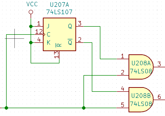
So how can you build such a signal ? Lets look at this simple circuit and analyze what is going on:
Lets input a clock on the JK flip-flop (pin 12). The JK is set with two active J and K signals, meaning that it will toggle its exits (Q at pin 3, inverse Q at pin 2) at each clock signal. Note that the 74LS107 triggers on the falling edge.
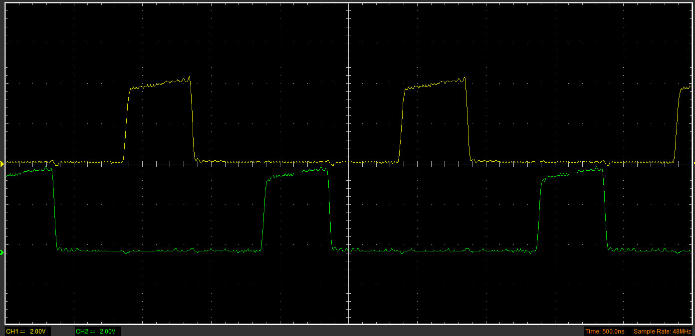
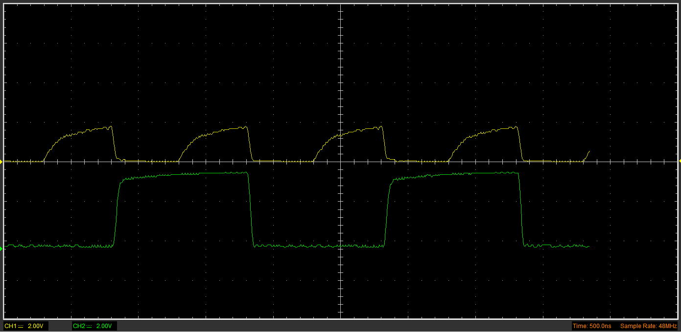
Below is the clock signal (pin 12 of the 74LS107, top signal) and the Q output (pin 3 of the 74LS107, bottom signal).
At each falling edge, the J-K flip flop toggles. It is therefore a frequency divider by 2. The output is half the frequency of the clock with a 50% duty cycle (ratio between high and low duration).
What happens then if we AND the clock and the Q output ?
Below is the graph of the clock signal (pin 12 of the 74LS107, top signal) and the output of the AND gate (pin 3 of the 74LS08, bottom signal):
We get the high part of the clock signal but only once out of two.
If at the same time, we AND the clock and the inverse Q we get the two reciprocating signals.
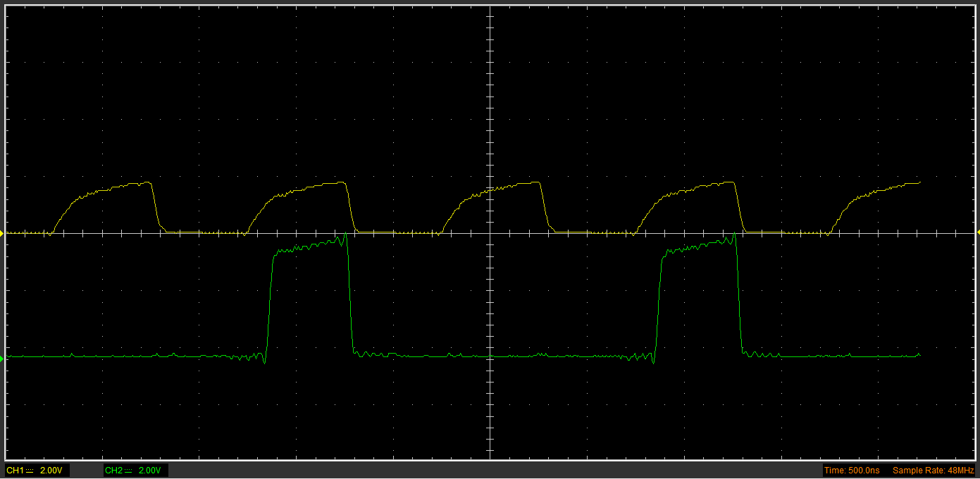
Below is the output of both AND gates (pin 3 of the 74LS08, top signal and pin 6 of the 74LS08, bottom signal) :
With such 2 clock signals, no chances that you will get a rising edge at the same time the other signal is high. The drawback however is that the clock is now half the frequency.
-
Setting / viewing the bus
11/05/2019 at 14:10 • 0 commentsSo we've been talking about the bus for some time. But when building a CPU we need two things from the bus:
- see what is going on (visualize the value currently set on the bus)
- manualy input a value if needed (for instance when trying to test a register, we need to set a known value on the bus to make sure the register can store it register_in and send it back register_out)
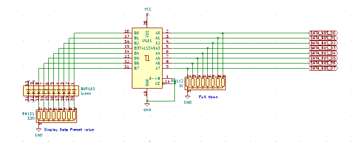
For this I have built a simple module that manually sets the value of the bus and displays the value of the bus.
However, there are a few contraints to take into account when building such a module:- You need to set a default value for the bus. if a line of the bus is kept hanging (not connected to anything), there are chances that you will get either random values or unexpected behavior. This is called terminating a bus. It is usually done by connecting each line of the bus to a known value (Ground or VCC - 0V or 5V) through a resistor (called pull down or pull up).
- It is not a good idea to plug LEDs directlly to the bus as they can draw many milliamps from the bus and eventually overload the IC that is active on the bus. To prevent that, a buffer was added (as usual a 74HCT245).
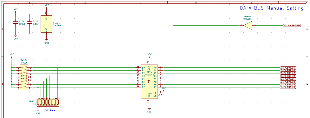
- We are using standard DIP switches to set a value, but as explained above, the value is actually not directly connected to the bus but with a 3-state buffer and an action signal
In the end this module is quite simple with only 2 74HCT245, a bunch of LEDs and resistor networks (it is easyer to use a resistor network than to manually plug 8 resistors).
[Note: do not forget the pull down resistors on the DIP switches otherwise the line would be seen as hanging when the switch is opened]
[note : the NAND gate is used as an inverter, juste because there was one available near the module]
Manual setting of the bus balue:
Displaying the Bus value and bus termination:
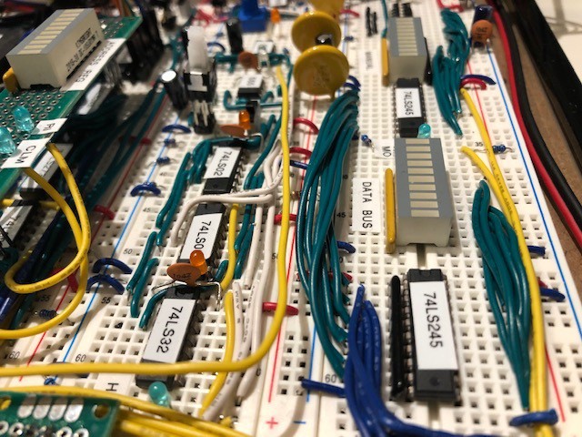
Preview of the Breadboard prototype (right of the photo):
![]()
-
Program Counter Register
11/05/2019 at 13:03 • 0 commentsOne register is very specific within the CPU: the Program Counter (PC).
Here is a definition of the Program Counter
So basically, if we read carefully the definition above, we understand that:
- A Program Counter is a register. It has the capability to store the information
- It has the capability to address the full scope of the memory that can store program (in some cases, program memory can be stored in a separate memory as data memory - otherwise it is shared memory and the PC can address the full scope of the memory). In our situation, it is shared memory and has 8-bit wide address.
- A Program Counter can be incremented (add 1 to the current value)
So for the Program Counter, there is need for a new action signal
- register_inc : this signal enables the automatic increment of the value of the register
The other action signals are the same as for a regular register:
- register_clear
- register_out
- register_in
[see log entry on Registers]
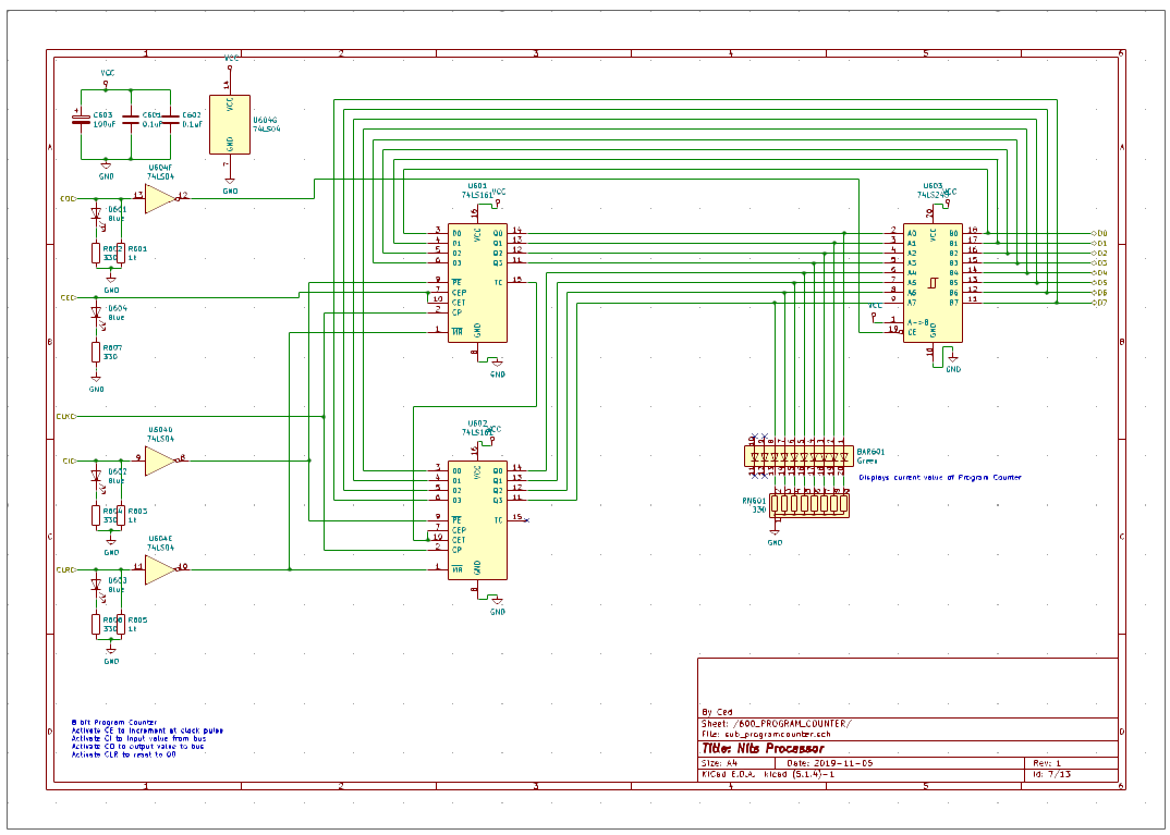
The IC used for our general purpose registers does not provide a way to increment the current value of the register. Increment could be implemented using gates but it is not such an easy task. Hopefully, there is an IC that provides just that:
- all the capabilities of a standard register (store, clear, input, output)
- a special signal to increment the value
However, the existing IC is 4 bits only, therefore we need to chain 2 ICs to provide an 8-bit register.
This IC is the 74HCT161:
- 4 bit inputs D0 to D3 (used to load the value of the register)
- 4 bit output Q0 to Q3
- 1 memory reset signal (master reset, this is an asynchronous signal in the 74161, synchronous in the 74163)
- 1 counter enable signal (synchronous, meaning that when active, the counter will be incremented at the next clock
- 1 clock signal (as usual the rising edge of the clock is used to synchronize the loading or the increment)
- 1 terminal count signal (this signal is used to chain 2 IC, when the 4 bit counter reaches the maximum value 1111, the TC signal is set to signal the next chip to increment)
- 1 parrallel in signal (this signal is used to load the value from the parrallel input)
When chaining two 74161, the TC signal is used to enable the counter of the next chip.
As for the general purpose register, the 74HCT245 is used as the 3-state output buffer.
As always, for learning purposes, the action signal are all set to active high and may need an inverter.
-
Registers - so many choices
11/05/2019 at 11:05 • 0 commentsCPUs are mainly temporary storage stuff with routing capabilites. To perform operations on data there is first the need to locally store this data (coming from memory, ROM or IOs) within the CPU.
There are even many types of registers in a CPU:
- general purpose registers (used to manipulate data)
- intruction registers (storing the instruction that is going to be executed)
- program counter (a special kind of counting register used to store at which step the program is currently positionned)
- address registers (pointers to memory)
- stack registers (also a pointer to memory but used for specific stack instructions)
- I/O registers used to communicate with external devices
- etc
Registers can vary in width depending on the CPU (from 8 bits to 128 bits). In our example they will all be 8-bit wide as we only have 8-bit data and 8-bit address capability.
In the following we only talk about the general purpose registers (couting registers will be discussed later).
So what are the functions of a general purpose register in the context of our CPU:
- load information from the bus when instructed to
- store the information until an action is performed or power is turned off
- display the information using LEDs
- 'publish' the stored information onto the bus when instructed to
- reset the information (or clear). This means putting all the bits to 0.
Therefore we can see there is the need for 3 signals to instruct the register what to do:
- register_in : load the information from the bus
- register_out : publish the information to the bus
- register_clear : clear the content of the register
However, something is key for a register : it's the timing of the loading function. Its has to be performed in a snapshot. This is why registers input the value from the bus on the rising edge of the clock. Therefore there is the need for 2 signals when inputing the values from the bus:
- the action signal register_in : the signal that informs the registers that it is going to load and store the information available at its input (usually the bus)
- the clock signal of wich we only use the rising edge to define the precise moment at witch the information is taken from the bus
There are many ICs in the 74xx series that provide some of these features (so many choices).
In Ben's videos, he uses the 74LS173 (4 bit register with output enable signal, input enable signal, clock and master reset signal)
[Update : See my later post on register IC]
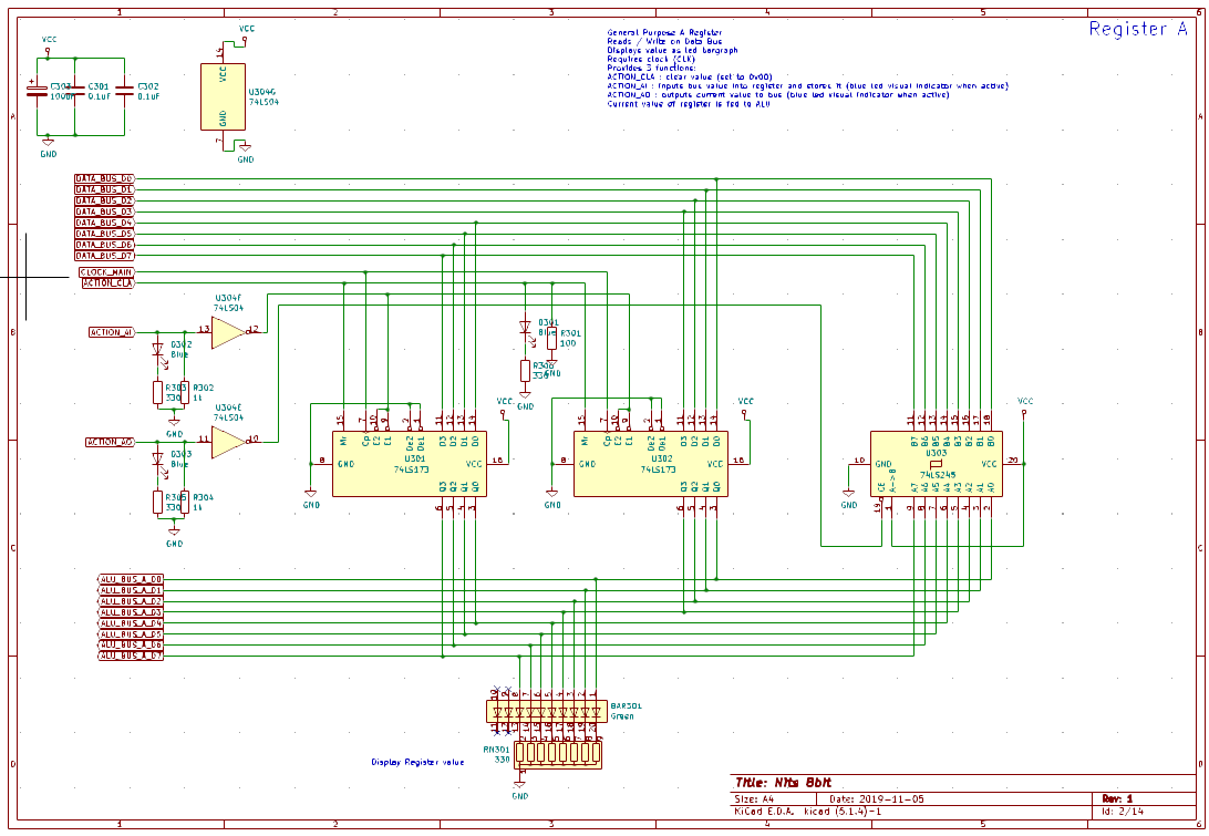
In practice we are not going to use the 3 state output and Output Enable capability of the 173 because we want to display the value of the register at all times on the LEDS. Therefore, the output is kept alway on. A separate chip is ised to provide the output buffering.
The 74HCT245 IC provides juste that : an octal buffer with 3 state output (it actually is bi-directional but we will use only one direction in this context). Note there is an existing single direction octal buffer, the 74HCT241 however the pinout is not as easy and in order to keep only one reference, we will use only the 245.
This chip offers 3 state output. This means that it can be seen as:
- output is activated and the value of the bit is 0 (0V)
- output is activated and the value of the bit is 1 (5V)
- output is deactivated and the chip is considered as not connected
So the outcome is that we need only 3 chips and a bunch of leds and resistors to implement a general purpose register.
Note that the diagram above shows 2 more elements not mentionned above : the link between the register and the ALU (out of topic for now) and some inverters on the action lines as the chips expect active low signals (this can be optimized later on, but for learning purposes it is better to show uniform active high action signals).
Preview of the prototype (using the original 74LS173 IC):
![]()
-
All about the clock module
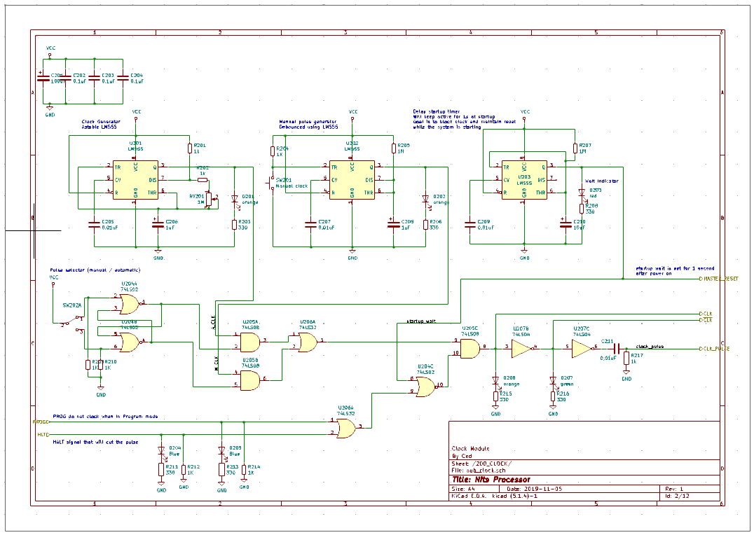
11/05/2019 at 09:28 • 0 commentsThe clock module is actually more complex than one would expect.
The main features are:
- Provide a clean clock signal (square wave), an inverse clock signal (square wave) and a pulse signal (on rising edge of the clock signal)
- Offer variable clock speed (between 0,75Hz to 500Hz) in order to see what is happening
- Offer manual clock to ensure a step by step analysis
- Offer a startup delay (2s) to block clock signal and send master reset signal
The clock module has two switches:
- Manual / Automatic clock selector (choose between automatic pulse with variable speed and a manuel push button)
- Clock pushbutton
It has two input signals:
- HALT signal will stop the clock signal (either in manual or automatic mode).
- PROG signal will stop the clock signal (when programming the RAM, avoid having the CPU continuing it's job)
It has 4 output signals:
- CLK : the clock signal. A square wave. Frequency can vary
- INVERSE CLK : the inverse of the clock signal.
- PULSE : a pulse signal derived from the CLK signal
- MASTER_RESET : this signal sends a global reset to all computer parts at startup to make sure the system is ready to run
It is mainly built using 555 timers and some logic.
- A 555 timer in Astable mode will provide the automatic clock. The potentiometer changes the time value.
- Minimum value (when potentiometer is at 0ohm) : Period = 0,693 x (1kohm + 2 x 1kohm) x 1uF = 0,693 x (1000 + 2000) x 0,000 001 = 0,002079.s That is a frequency of 481Hz
- Maximum value (when potentiometer is at 1Mohm) : Period = 0,693 x (1kohm + 2 x 1Mohm) x 1uF = 0,693 x (1000 + 2 000 000) x 0,000 001 = 1,38s. That is a frequency of 0,72 Hz
- A 555 timer is monostable mode will provide the manual switch debouncing (to prevent bounce effect when switch is activated). When switching it will turn on the 555 time for a pre-defined period and it will turn off again, only once. The timer will stay on for a period defined by : period = 1,1 x 1Mohm x 1uF = 1,1 x 1 000 000 x 0,000 001 = 1,1s
- A 555 timer will provide the startup delay. When power is turned on, 555 is immediately set to on, until the capacitor is charged and then it turns off permanently. Period is defined using the same rule as the monostable above. Delay is 1s.
A few elements of logic are used to provide a clean signal and a debounced switch between the manual and automatic:
- Debouncing is performed using an SR latch with two NOR gates.
- Signal is output only if the following is TRUE : NOT (startup_wait | PROG | HALT)
- INVERTED CLOCK signal is provided using an inverter
- Pulse signal is provided using a RC with a time constant of period = 0,01uF x 1kOhm = 0,000 000 01 x 1000 = 0,000 01 s. Warning : the RC is positionned after a second inverter in order to buffer its effect and prevent poluting the clock signal. Also the double inverter gates provide a small delay compared to the actual rising edge of the clock signal.
Other chips used in this clock module:
- 74HCT02: provides four 2-input NOR gates
- 74HCT08: provides four 2-input AND gates
- 74HCT32: provdes four 2-input OR gates
- 74HCT04: provides six NOT gates (inverters)
Finally a few leds are positonned to show the actual status of each element:
- orange led show clock signal (automatic, manual, output)
- red led show the startup wait status
- blue led show action signals (HALT, PROG)
- green led show inverted clock signal
View of the prototype:
![]()
-
Design Principles
10/31/2019 at 16:49 • 0 commentsHere are a few design principles:
- The main objective is the learning experience. Therefore optimisation is not the goal neither in component count nor in performance. Anyway when building a TTL base computer, performance cannot be the goal.
- All components are 74LS or 74HCT series bought new
- All is positive logic.
- Leds are put eveywhere the undestanding of the inner workings is required (bus, status, actions signals, register values, etc). Leds are the better and easy way to display signals. Each led is protected by a 330ohm resistor (5v power supply, 1,4V drop at the led. Therefore 3,6V at the led level. With a 330ohm resistor it allows for a 10mA current)
- When needed pullup or pulldown resistors are 1kohm
- Each IC as a 0,1uF capacitor close to it for decoupling and power reserve
- Each power line has a 100uF capacitor as a power reserve
 Ced
Ced