 Jared Sanson
-
OLED Breakout
10/29/2019 at 06:03 • 0 commentsHere is the breakout board that came with my unit:
This consists of a specialized OLED driver chip, a 2.8v LDO, and two OLED connectors that utilize only 1 MIPI data pair on each channel:
I was unable to find a datasheet for my specific displays, but I determined the pinout for each display is roughly:
-
MCU
10/29/2019 at 05:25 • 8 commentsAs explained in previous logs, the MCU is the brain of the board. It configures the HDMI bridge chip, and handles power-sequencing of the display.
Out of curiousity, I connected an STLink to the SWD pads on the PCB, and behold, the chip is unlocked!
This allowed me to extract the firmware. I plan to reverse-engineer the firmware to determine how it configures the system, and how it could be configured via USB.
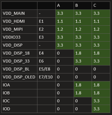
GPIO map:
---------- more ----------Label
MCU Pin
MCU Port
Net Name
Supply Voltage
E1
31
PA10
VDD_HDMI
1.1v
E2
14
PA4
VDD_MIPI
1.2v
E3
11
PA1
VDD33_HDMI VDDIO33
3.3v
E4
30
PA9
VDD_DISP_18
1.8v
E5
42
PB6
VDD_BL (V3)
?
E6
13
PA3
VDD_DISP_33
3.3v
E7
17
PA7
VDD_OLED (V1/V2)
+V/-V?
E8
43
PB7
VDD_BL (V3)
?
E9
45
PB8
Feedback?
?
E10
29
PA8
VDD_OLED (V1/V2)
+V/-V?
L1
16
PA6
LED1
L2
15
PA5
LED2
A
21
PB10
IOA (1.8v)
B
46
PB9
IOB (1.8v)
C
25
PB12
IOC (3.3v)
D
22
PB11
IOD (3.3v)
B1
28
PB15
BTN1 (Left)
B2
27
PB14
BTN2 (Right)
(Ignore the labels column - I am using it within my reverse engineering to track the signals)
Flash Layout
0000 0000
Boot Space (Aliases to one of the below regions)
0800 0000
Flash space
1FFF F000
System memory space
2000 0000
SRAM space
1FFF F7D6
USART Bootloader
-
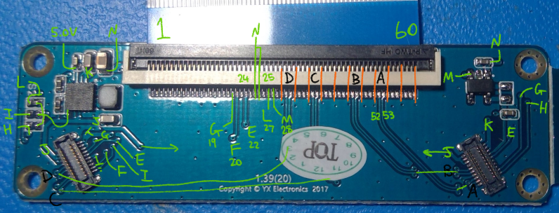
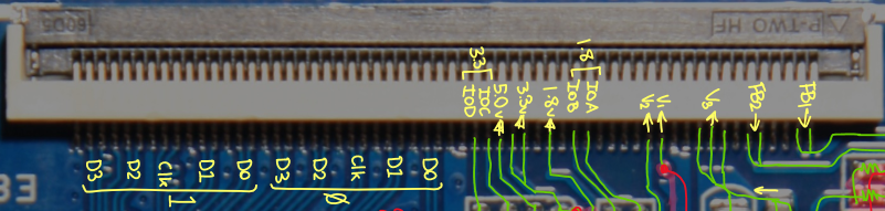
Display Connector
10/29/2019 at 05:19 • 0 comments![]() The connector provides two independent MIPI channels, each with 4 data pairs & 1 clock pair. The 5V rail is always powered, but the other rails can be individually sequenced and controlled by the MCU. The GPIOs can be used to control additional regulators or enable control signals on the display board. They are output only.
The connector provides two independent MIPI channels, each with 4 data pairs & 1 clock pair. The 5V rail is always powered, but the other rails can be individually sequenced and controlled by the MCU. The GPIOs can be used to control additional regulators or enable control signals on the display board. They are output only.---------- more ----------
I do not know what chip "ET7" and "MH 23 22" are, but they are obviously some kind of buck regulator. A/B/C/D are the GPIO control signals from the MCU (output only).
E6 enables the 3.3v rail, and supplies the 1.8v regulator. IOC/D are powered even if this rail is not.
E4 enables the 1.8v rail to the display connector, but only if E6 is also enabled (for 3.3v). IOA/B are pulled-up to 1.8v if this is enabled.
The 5V rail is always powered.
I am not sure what the deal is with the chip at the top that is fed directly from +5v.
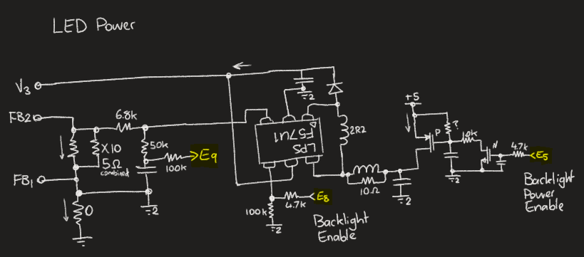
TFT Backlight Driver
For TFTs, there is a dedicated backlight driver:V3 is +V for the backlight, and either FB1/2 can probably be chosen for -V depending on the drive strength that is desired.
E9 is obviously an analog feedback signal to the MCU for controlling the drive current, E5 is the main supply enable, and E8 is probably a PWM control signal for defining the drive current.
OLED Bias VoltageE7 enables the bias circuit.
E10 is probably a PWM drive signal for controlling display brightness.
On my board, the following signals come up in this order when it is powered on:A: Slow Flashing Blue LED / Initial power-up
B: Fast Flashing Blue LED
C: Green LED
You can see that on my board, the LED backlight & OLED bias supplies are never turned on. Instead the dsplay board has it's own regulators which are controlled by the IOA/B/C/D GPIOs.
Full connector pinout:Number
Net Name
Voltage
Breakout Net
Use
Description
1
FB1
Feedback 1
2
FB1
Feedback 1
3
-
4
-
5
FB2
Feedback 2
6
FB2
Feedback 2
7
-
8
V3
Backlight
9
V3
Backlight
10
V3
Backlight
11
-
12
GND
13
V1
OLED Bias (E7+E10 Ctrl)
14
V2
OLED Bias (E7+E10 Ctrl)
15
-
16
-
17
-
18
-
19
IOA
1.8
G
Right OLED Enable?
E4 Ctrl
20
IOB
1.8
F
Right OLED Enable?
E4 Ctrl or Always powered?
21
-
22
V_1.8
1.8
E
1.8v Supply
E4 Ctrl
23
-
24
V_3.3
3.3
N
3.3v Supply (1st)
E6 Ctrl
25
V_3.3
3.3
N
3.3v Supply (1st)
E6 Ctrl
26
V_5.0
5.0
USB VIN, Always powered
27
IOC
3.3
L
Enable OLED Bias (2nd)
Always powered
28
IOD
3.3
M
Enable 2.8v Supply (1st)
Always powered
29
-
30
GND
31
DSI0_D0
D
32
DSI0_D0
D
33
GND
34
DSI0_D1
35
DSI0_D1
36
GND
37
DSI0_C
C
38
DSI0_C
C
39
GND
40
DSI0_D2
41
DSI0_D2
42
GND
43
DSI0_D3
44
DSI0_D3
45
GND
46
DSI1_D0
B
47
DSI1_D0
B
48
GND
49
DSI1_D1
50
DSI1_D1
51
GND
52
DSI1_C
A
53
DSI1_C
A
54
GND
55
DSI1_D2
56
DSI1_D2
57
GND
58
DSI1_D3
59
DSI1_D3
60
GND
-
Board Overview
10/29/2019 at 05:17 • 0 commentsTo start reverse-engineering the circuit behind this board, I started by taking photos of the bottom and top layers, and inking over with my Surface:
![]() ---------- more ----------
---------- more ----------MIPI-HDMI Bridge Chip
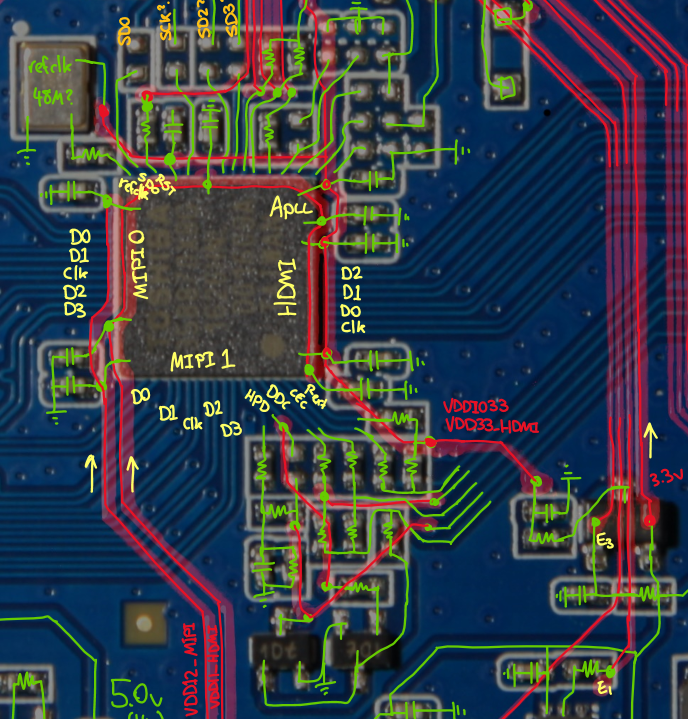
You can see that the connector on the right does indeed support two MIPI channels, each consisting of 4 data pairs & 1 clock pair. The MIPI bridge chip is connected to the MCU via I2C, and there is minimal support circuitry (only a crystal, a few buck regulators, and some passives for the PLL).
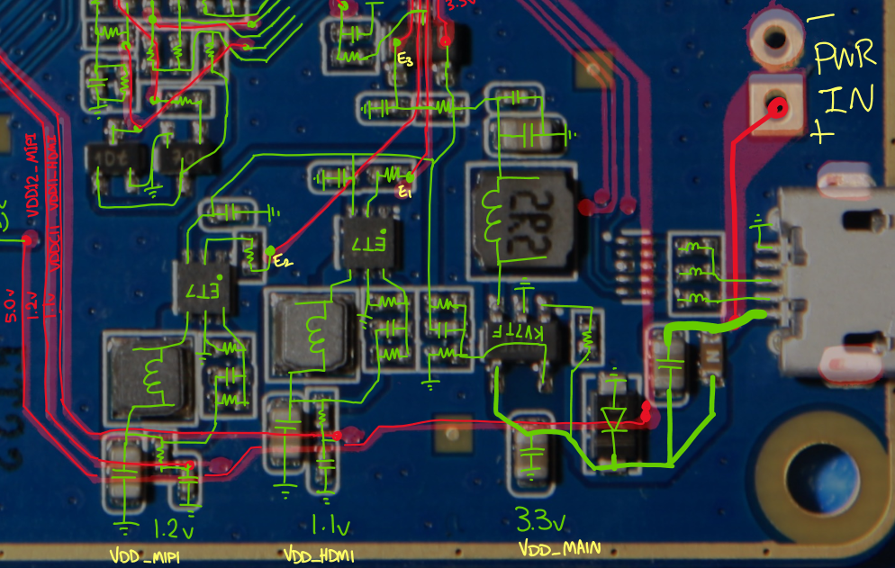
Main Buck Regulators
On the bottom-right you can see the main buck regulators which supply power to the MIPI bridge chip. 5.0V is fed onwards to the display buck regulators elsewhere on the PCB.E1 controls the 1.1v supply for the MIPI bridge (VDDC11, VDD11_HDMI)
E2 controls the 1.2v supply (VDD12_MIPI)
E3 controls the 3.3v supply for the MIPI bridge (VDDIO33, VDD33_HDMI), and the MCU & Audio circuit. I believe this defaults to on, and allows the MCU to power down the system.
The Display & IO has an always-on 3.3V supply (DISP33)
OLED SuppliesOn the upper-left you can see that things get a bit more complicated. A lot of this is to support many different kinds of displays, and provides various voltages for backlighting, OLED biasing, etc. It also supples two sets of bi-directional GPIOs, one at 1.8V, and one at 3.3V.
For more information on how this works, see the next project log.
MCU
Finally we have the "STM32" MCU which is the brains of the board:
Those four pads on the right look interesting... could they be SWD perhaps?
(VDD, GND, PA13/SWDIO, PA14/SWCLK)
MIPI-HDMI Bridge RE
Reverse-Engineering a random MIPI-HDMI bridge from China
 This consists of a specialized OLED driver chip, a 2.8v LDO, and two OLED connectors that utilize only 1 MIPI data pair on each channel:
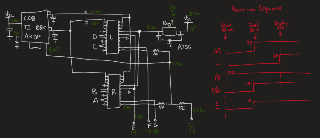 I was unable to find a datasheet for my specific displays, but I determined the pinout for each display is roughly:
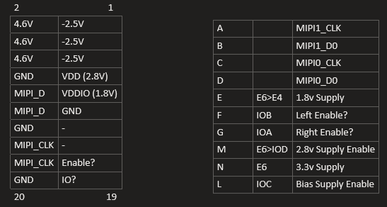
 The connector provides two independent MIPI channels, each with 4 data pairs & 1 clock pair. The 5V rail is always powered, but the other rails can be individually sequenced and controlled by the MCU. The GPIOs can be used to control additional regulators or enable control signals on the display board. They are output only.
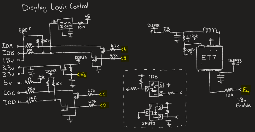
 V3 is +V for the backlight, and either FB1/2 can probably be chosen for -V depending on the drive strength that is desired.
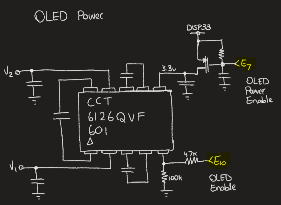
 A: Slow Flashing
Blue LED / Initial power-up
A: Slow Flashing
Blue LED / Initial power-up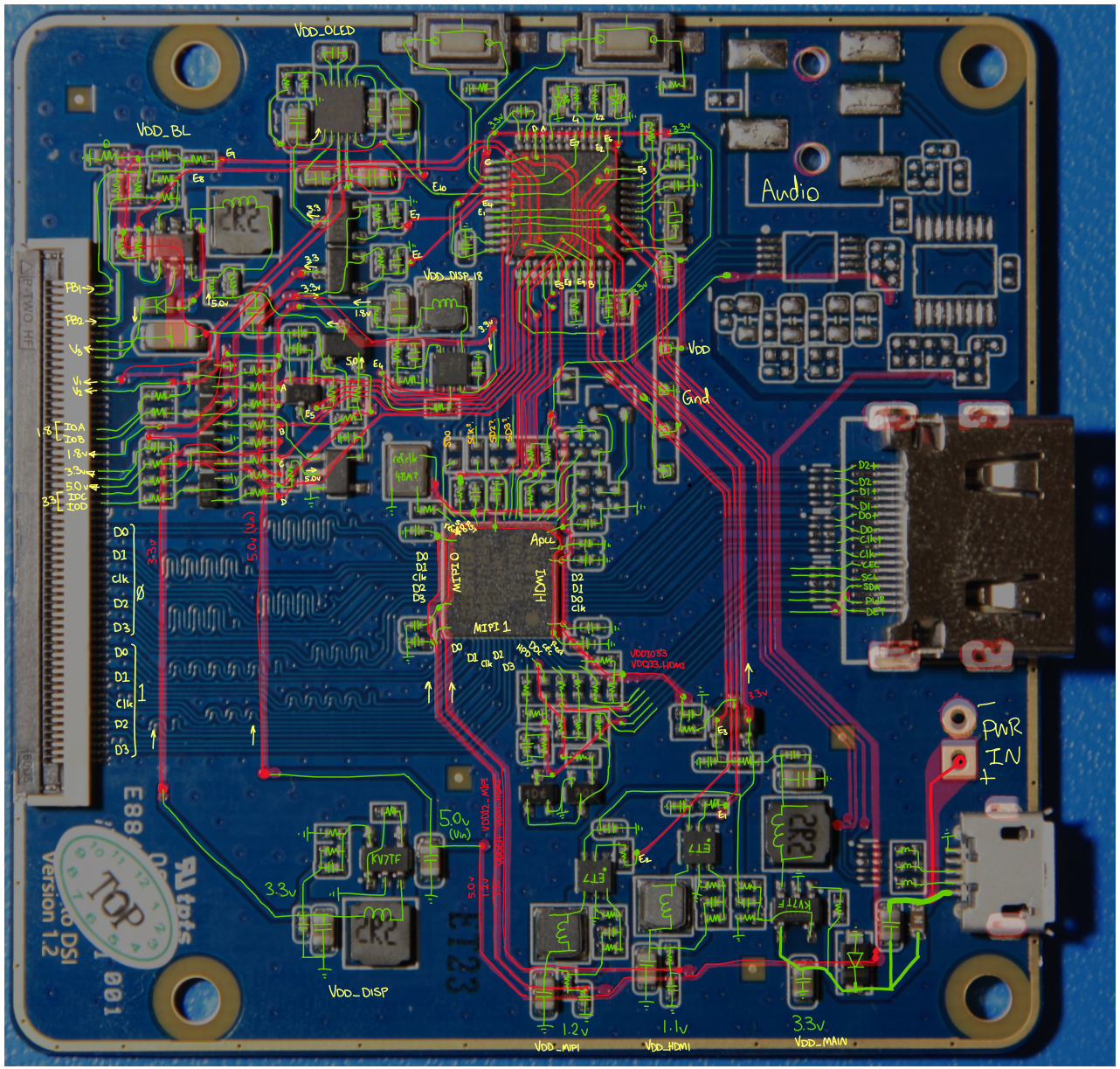
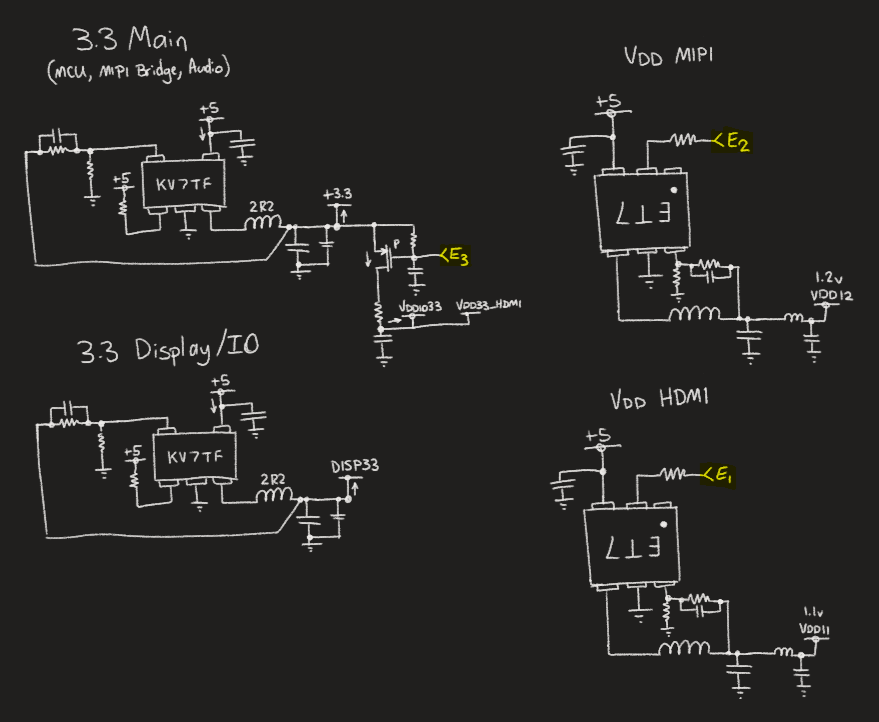 E1 controls the 1.1v supply for the MIPI bridge (VDDC11, VDD11_HDMI)
 For more information on how this works, see the next project log.
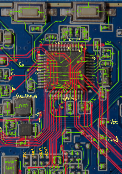 Those four pads on the right look interesting... could they be SWD perhaps?