-
Selective Stencil Soldering
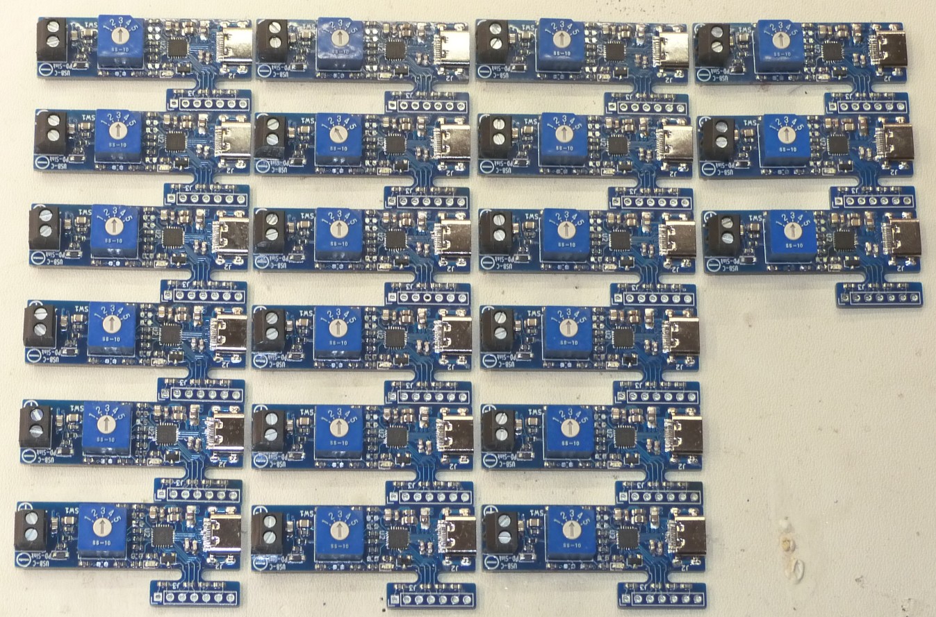
08/12/2022 at 01:32 • 0 commentsJust like everybody else, the chip shortage has caught up to me sooner or later. The controller chip CYPD3177 for my USB-C Power delivery (PD) sink was out of stock everywhere for several months. So I decided to order boards populated with everything except the chip (and some of them also without the switches as they were short on stock as well). Sometimes the quick turn assembly houses only stencils solder paste onto the pads of the populated components, no matter what the provided Gerber paste layer looks like. With this in mind I tried to come up with a new (for me) method to apply paste for re-flowing the chip.
When the IC was available again I bought enough to finish all the boards and put them in stock in my Tindie store.
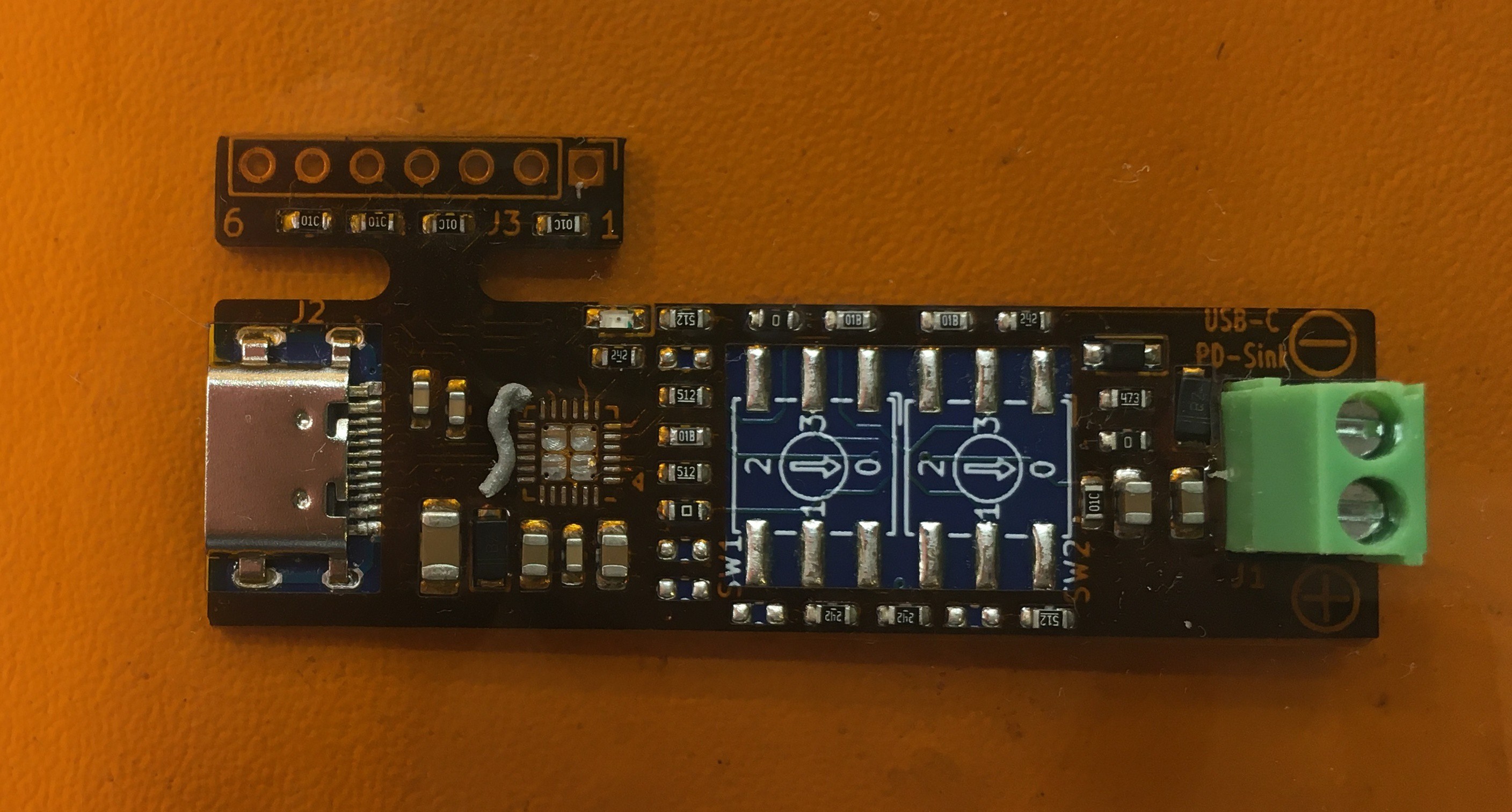
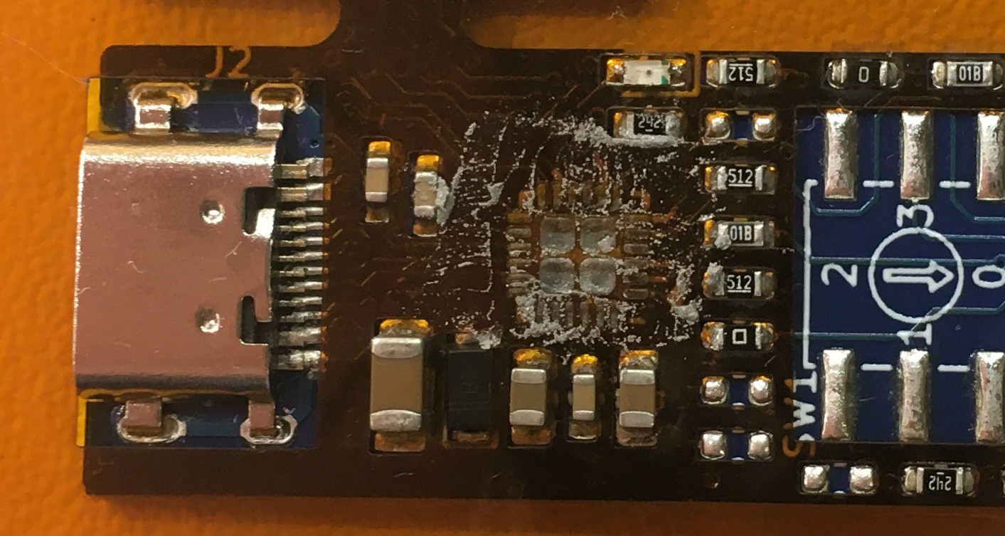
Enter the "selective solder stencil". I created a new paste layer and left only the chip pattern as intended to have the pin pads and the bottom center pad open. For all other components I created openings as big as the perimeter of component body+ solder pads. This enables the stencil to slide over already populated components and as a nice side effect being perfectly centered over the empty footprint. I ordered the stencil from OshStencils, as Polyimide film. A thin strip of cut credit card served as paste squeegee to spread the paste only in the desired area. Lifting the stencil left the paste in the correct place. The distribution was not perfect due to the fact that the polyimide stencil was not perfectly flat but bowing up a little. But during re-flow/hot air soldering, the solder usually knows where to go to build nice solder joints and no bridges.
For this try I used hot air for soldering as the screw terminal would not be happy about excessive time on the hot plate. Everything went smooth and the board worked perfectly as expected.
This exercise remained a proof of concept, as the board house was so kind to also put solder on the un-populated pads, which made the whole process easier. Putting down some sticky flux was enough to activate the existing solder and connect the chip just as good as with fresh paste. Next time I would make the opening maybe 1 or 2 mil (25 um or 50 um) wider to give some tolerance to the whole process.
Here are some pictures to demonstrate the steps from empty board to finished assembly:
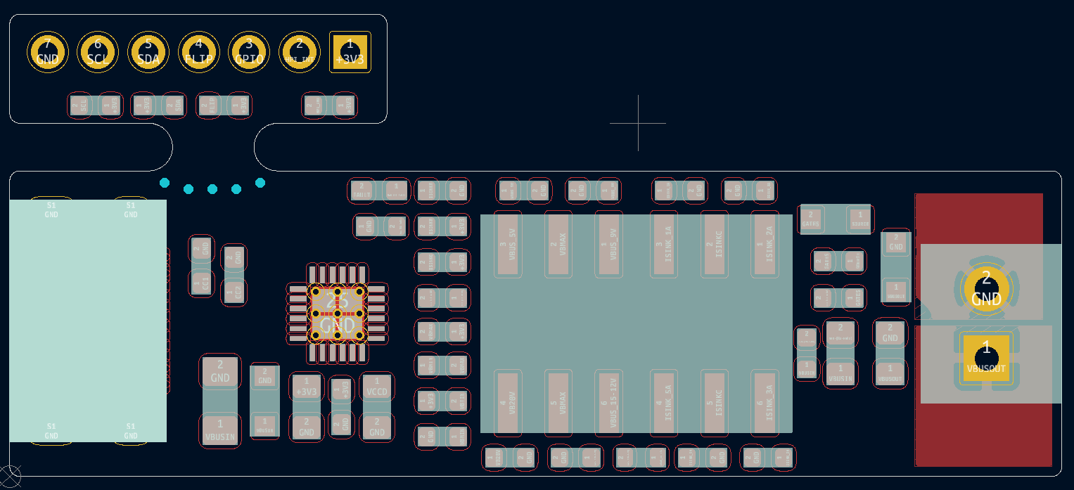
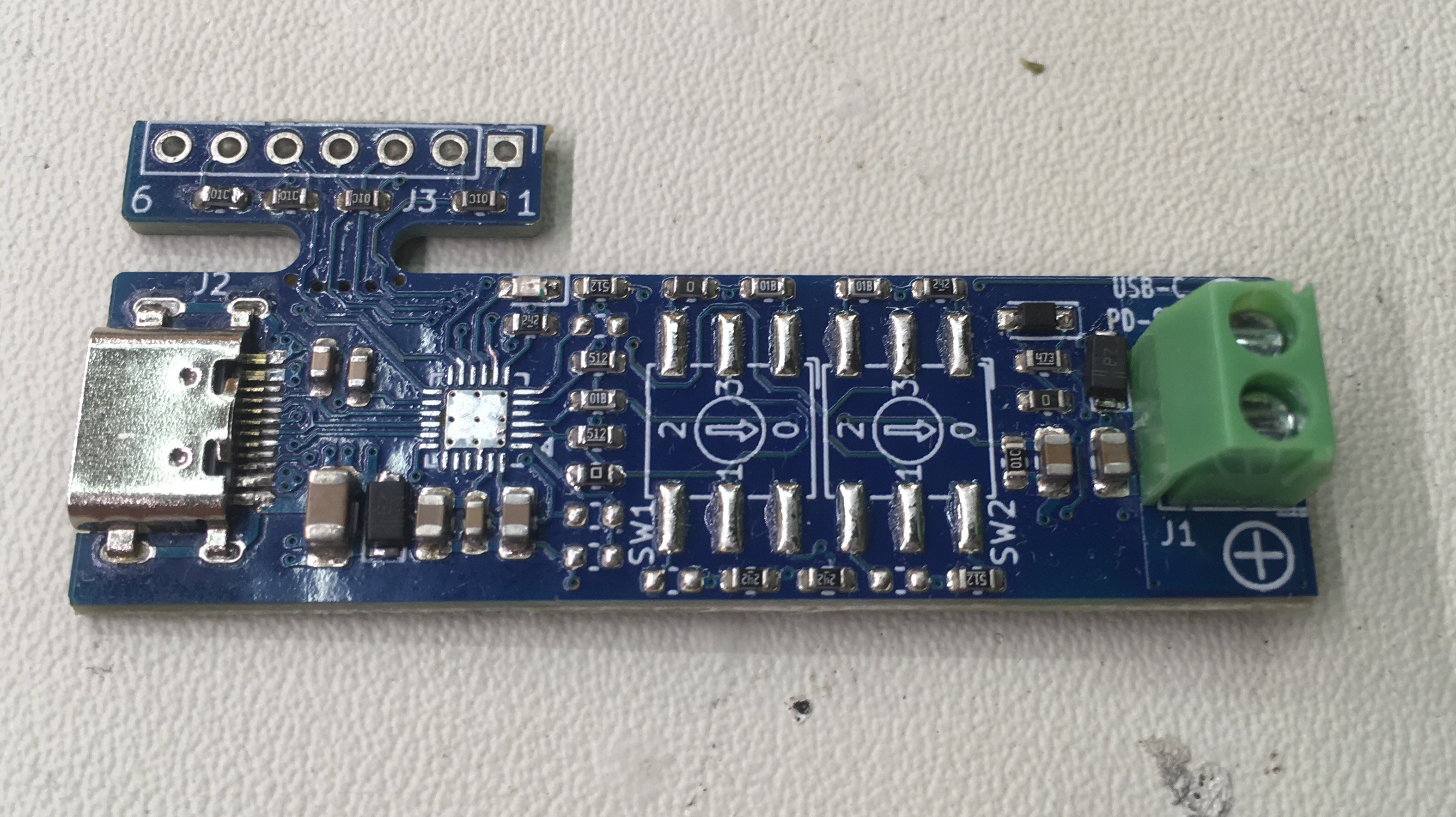
This is how the KiCAD design looks like; light blue is the selective solder stencil layer with the red pads shining through.
![]()
The partly assembled board with a clean footprint for the chip to be populated![]()
The orange stencil placed over the board. The already assembled components are sticking nicely through the openings. A somewhat enough amount of paste is ready to be spread over the footprint.
![]()
Solder is squeezed into the stencil openings.![]()
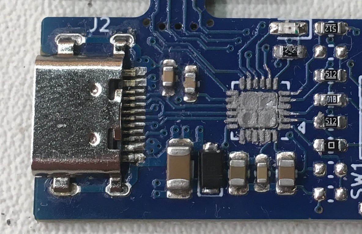
The pasted board without the stencil ready to have the chip placed onto the pads.
![]()
And the finished board:
![]()
-
USB-C Power Delivery for every RPi
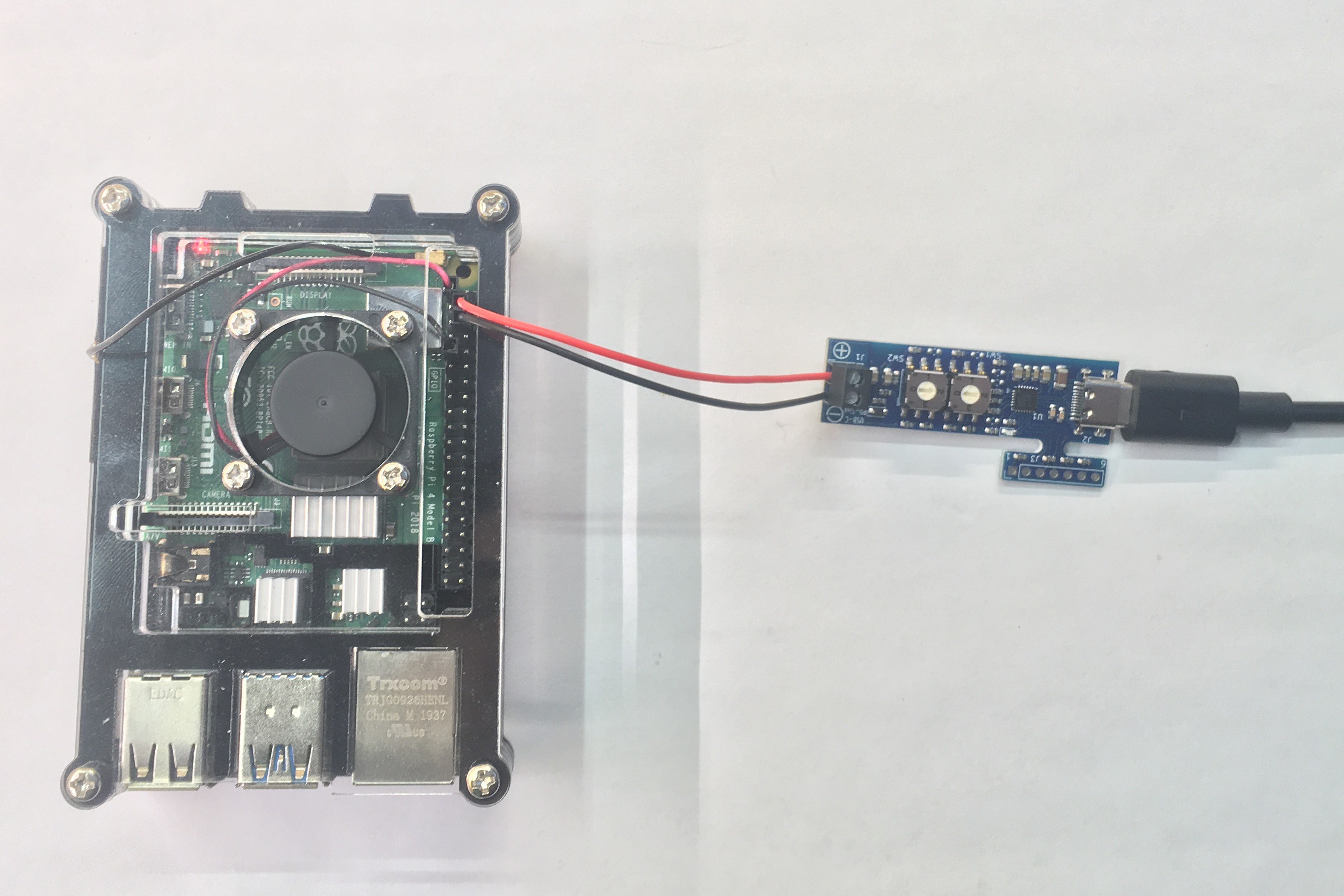
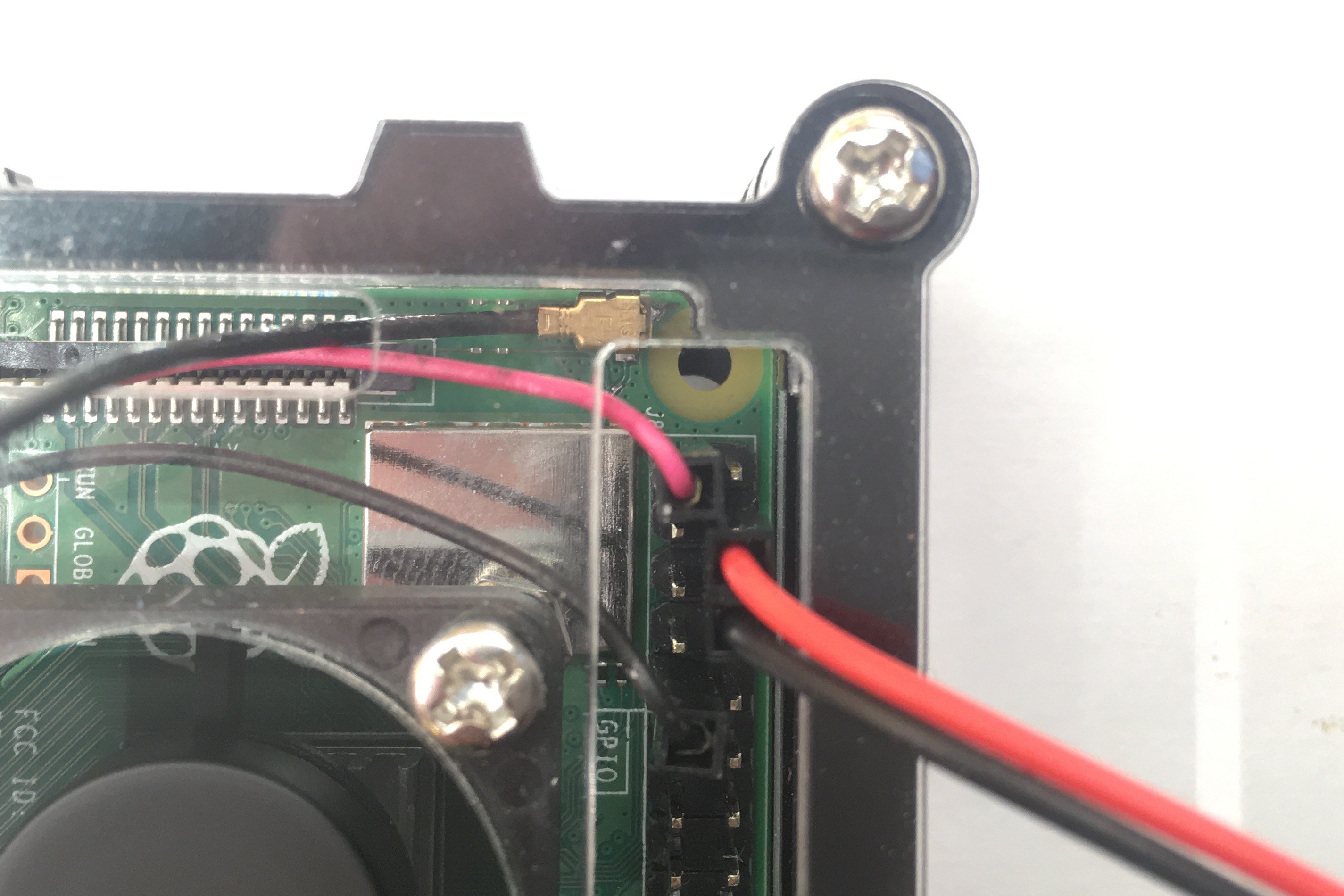
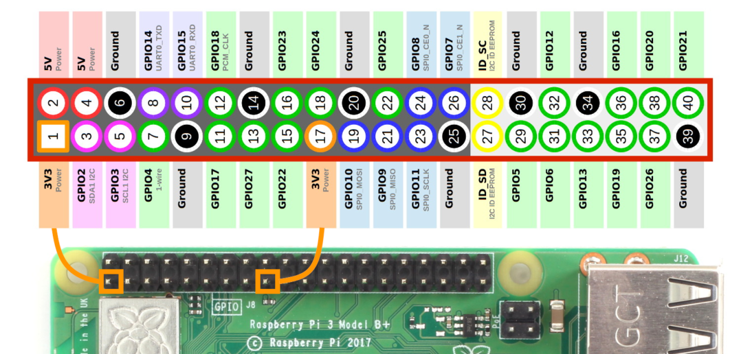
03/07/2021 at 01:46 • 0 commentsWith the USB-C PD Sink board, it is possible to power every RPi (except the RPi 400) with a USB PD power supply. The board is set to 5V (switch S1 on pos 0) and 3A (switch S2 on pos 2) and connected to the RPi 40 pin HAT connector through a 2-pin header. On this header pin 4 for +5V and pin 6 for ground is used.
![]()
A detail picture of the connector. The red and black wire to the right are the power supply. For reference, the red and black to the left are the fan of the enclosure.![]()
And for more reference, here is a generic HAT header pinout (courtesy RPi foundation website).![]()
A word of caution: connecting power to the wrong pins or having the PD board set to a voltage higher than 5V will cause permanent damage to the RPi. Only try this at home when you know what you are doing. And then do it right. Check and check again, and check on more time.And don't mind the UMC connection on the RPi, that is a story for a different time.
-
Selecting the right FET
11/08/2020 at 02:34 • 0 commentsSelecting the right FETs as the power switch is important, when switching 5A at 20V.
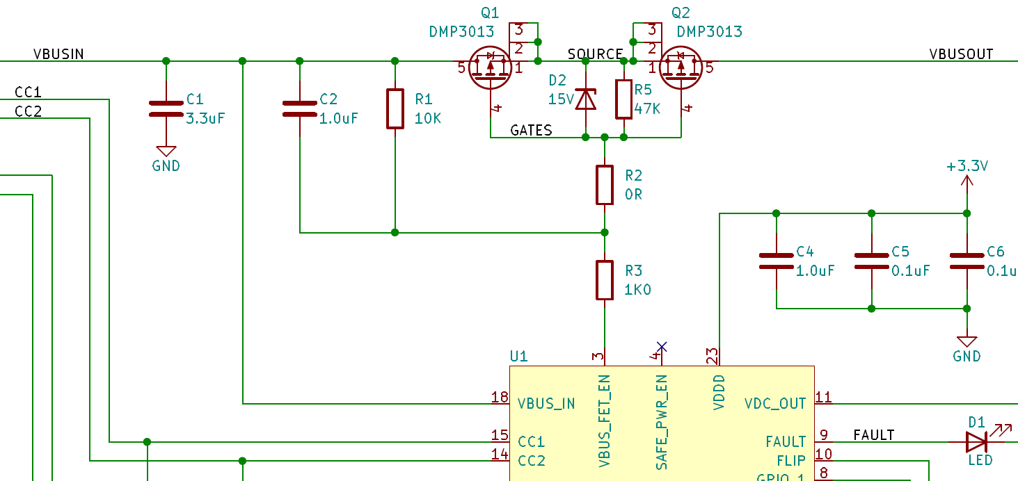
My initial pick was the Alpha & Omega AON7407. It has very good Rds_on but was lacking at V_drain-source with only -20V max and V_gate-source of only 8V. Better candidates turned out to be:
Diodes DMP3013 with V_ds = -30V and V_gs = 25V; Rds_on 9.5mOhm (V_gs=10V)
Rohm RQ3E120 with V_ds = -30V and V_gs = 20V; Rds_on 8.8mOhm (V_gs=10V)
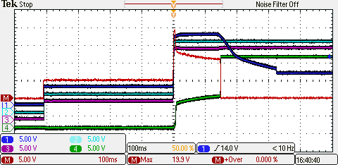
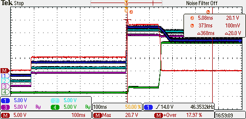
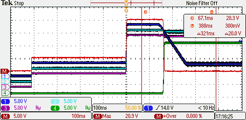
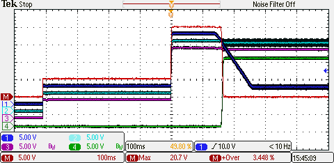
The following scope plots all show:
Ch1: signal GATES
Ch2: signal VBUSIN
Ch3: signal SOURCE
Ch4: signal VBUSOUT
Math: Ch3 - Ch4 = SOURCE - VBUSOUT to measure Vds
The 1st step to 5V is the initial USB power up, the trigger point is the successful power contract negotiation (blue,light blue and purple trace rise to 20V) and~140msec later, the FETs finally turn on(green trace starts raising) and the input voltage drops slightly because of the 4.85A current draw.
Q1, Q2 = AON7407:
Q1, Q2 = AON7407 with D2 = 7.5V Zener Diode:
Q1, Q2 = Diodes DMP3013:
Q1,Q2 = Rohm RQ3E120:
The AON7404 shows a weird pulse on the math channel when USB-VBUS turns on to 20V and the turn on cycle with 15V gate voltage is not really smooth.
The Diodes and Rohm FETs behave identical with proper turn on cycles.
In the end I decided to use the Diodes DMP3013, as it has extra gate protection diodes built in. -
Power FET Diodes DMP3013
10/28/2020 at 01:13 • 0 commentsAnd then I found an even better FETs that has a Rds_on of only 9.5 mOhm (at Vsg = 10V), which is just as good as the previous one as Vsg >10 V at the output setting of 12V or more.
This FET is the Diodes DMP3013SFV. same 3.3mm x 3.3mm footprint.
And I did a measurement with 19 boards, which showed to real Rds_on to be 7.3 mOhm onaverage, because the Vsg is ~15V at the 20V setting. Also the calculated junction temperature is quite low and much more manageable now.
Results (still fixed width font anybody?):
Vfet*2 Vload I load P load P fet Tjunc Rds on
70.5 19.47 4.87 94.77 0.343 46.4 0.0072
71.04 19.61 4.90 96.14 0.348 46.8 0.0072
70.7 19.62 4.91 96.24 0.347 46.7 0.0072
72.8 19.59 4.90 95.94 0.357 47.3 0.0074
70.6 19.64 4.91 96.43 0.347 46.7 0.0072
72.4 19.64 4.91 96.43 0.355 47.2 0.0074
71 19.66 4.92 96.63 0.349 46.8 0.0072
69.4 19.67 4.92 96.73 0.341 46.3 0.0071
72.8 19.63 4.91 96.33 0.357 47.3 0.0074
73.1 19.62 4.91 96.24 0.359 47.4 0.0075
71.4 19.61 4.90 96.14 0.350 46.9 0.0073
69.9 19.63 4.91 96.33 0.343 46.4 0.0071
72.9 19.64 4.91 96.43 0.358 47.4 0.0074
70.8 19.62 4.91 96.24 0.347 46.7 0.0072
71.3 19.64 4.91 96.43 0.350 46.9 0.0073
73.6 19.6 4.90 96.04 0.361 47.5 0.0075
72.3 19.61 4.90 96.14 0.354 47.2 0.0074
71.9 19.61 4.90 96.14 0.352 47.0 0.0073
74.7 19.64 4.91 96.43 0.367 47.9 0.0076
Average: 0.0073 -
New FETs with lower Rds_on
08/17/2020 at 02:18 • 0 commentsTime passes...
I finished the design of Rev4 (and Rev3 in between). Most important improvement is a 2nd switch to select the current and new switching FETs . The new FETs have a Rds_on of only 9.5 mOhm (at Vsg = 4.5V), which cuts the dissipation almost in half and keeps the board cooler, even with 5 A current draw.
This FET is the AON7407.
And I did a measurement with 24 boards, which showed to real Rds_on to be 7.1mOhm onaverage, because the Vsg is ~15V at the 20V setting. Also the calculated junction temperature is quite low and much more manageable now.
Results (fixed width font anybody?):
Vfet*2 Vload I load P load P fet Tjunc Rds on
73.3 19.55 4.89 95.55 0.358 47.4 0.0075
72.5 19.58 4.90 95.84 0.355 47.2 0.0074
70.2 19.6 4.90 96.04 0.344 46.5 0.0072
69.3 19.6 4.90 96.04 0.340 46.2 0.0071
71.2 19.55 4.89 95.55 0.348 46.7 0.0073
68.6 19.65 4.91 96.53 0.337 46.1 0.0070
71.2 19.59 4.90 95.94 0.349 46.8 0.0073
68.1 19.68 4.92 96.83 0.335 45.9 0.0069
69.7 19.67 4.92 96.73 0.343 46.4 0.0071
68.5 19.67 4.92 96.73 0.337 46.1 0.0070
68.4 19.7 4.93 97.02 0.337 46.1 0.0069
68.7 19.7 4.93 97.02 0.338 46.1 0.0070
72.8 19.69 4.92 96.92 0.358 47.4 0.0074
69.5 19.71 4.93 97.12 0.342 46.4 0.0071
70.6 19.71 4.93 97.12 0.348 46.7 0.0072
68.3 19.72 4.93 97.22 0.337 46.0 0.0069
68.4 19.71 4.93 97.12 0.337 46.1 0.0069
70.7 19.71 4.93 97.12 0.348 46.8 0.0072
71.1 19.7 4.93 97.02 0.350 46.9 0.0072
68.4 19.7 4.93 97.02 0.337 46.1 0.0069
70.2 19.68 4.92 96.83 0.345 46.6 0.0071
73.5 19.68 4.92 96.83 0.362 47.6 0.0075
68.4 19.7 4.93 97.02 0.337 46.1 0.0069
70.6 19.7 4.93 97.02 0.348 46.7 0.0072
Average: 0.0071PS: I just could not bring myself to copy every single cell into the table here.
-
Production
02/17/2020 at 12:31 • 1 commentProduction at home for the next batch went very well but slow. How I have to set up a larger supply chain.
![]()
OCD anybody :)
-
Break off tabs
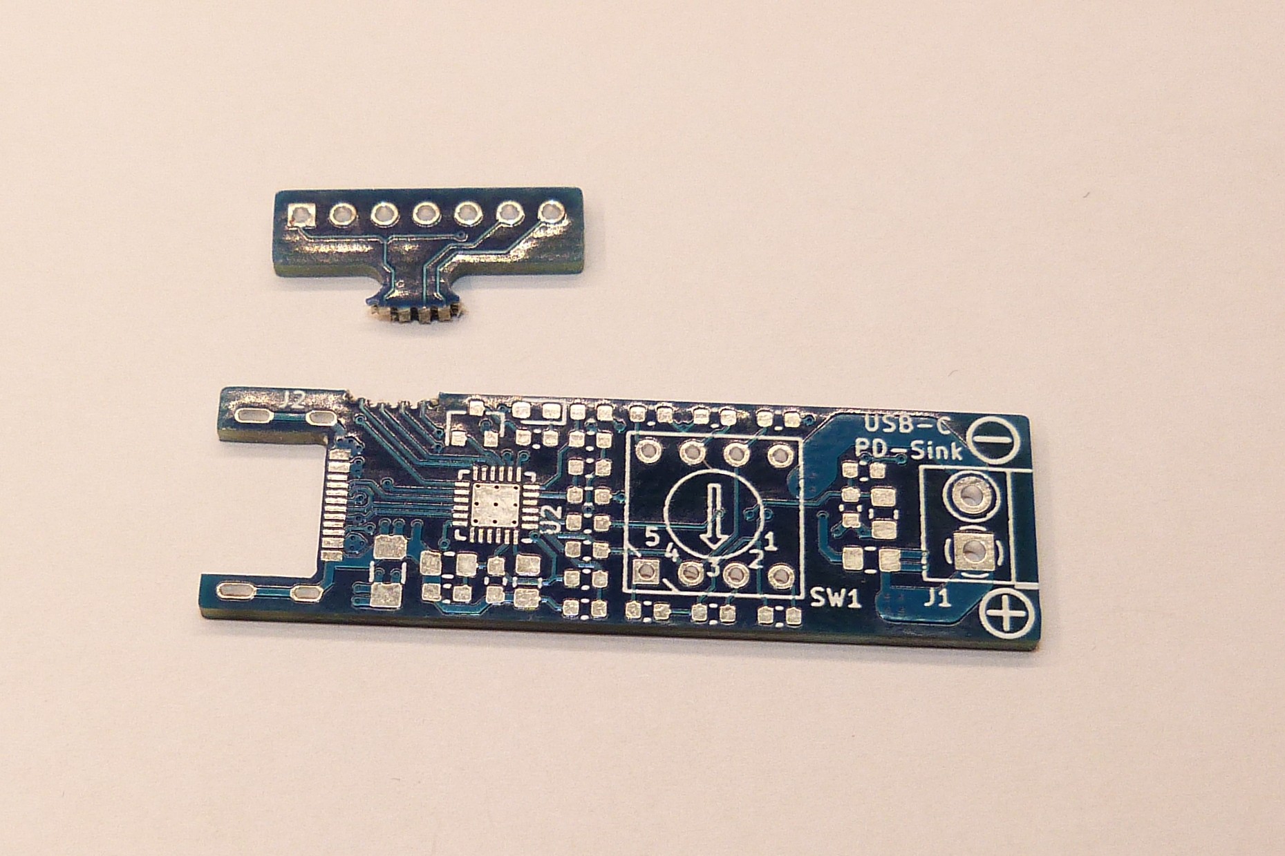
02/02/2020 at 01:06 • 0 commentsThe break-off tab for the telemetry connector seems to be working as planned. I tested it with a bare board and it snapped right off. For a populated board I would recommend to score a line along the holes on both sides first to put a little less stress on the components nearby.
![]()
-
The heat is on.
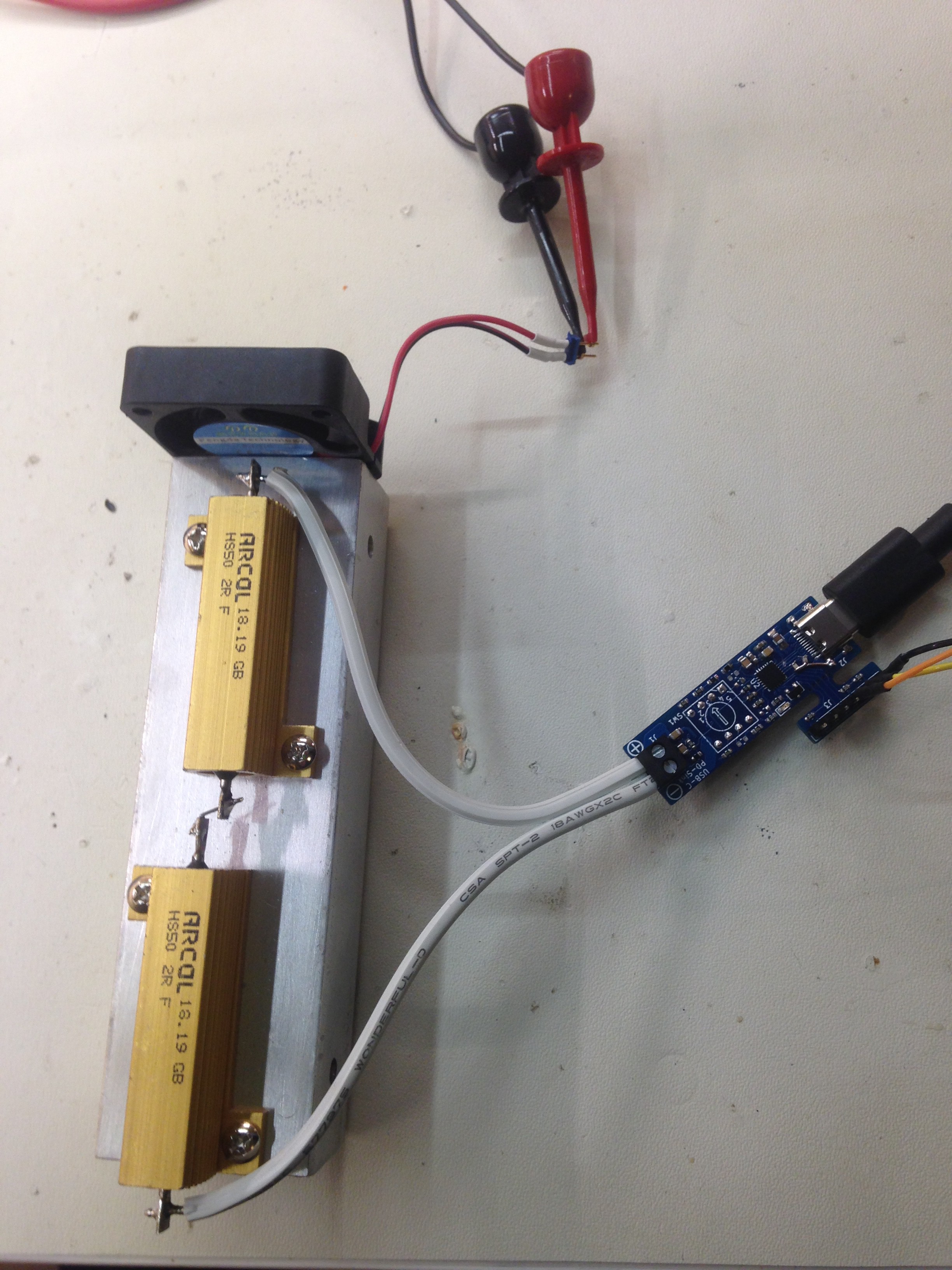
12/18/2019 at 02:03 • 0 commentsI have built a load to test the power draw of the board. It is 2x 2Ohm 50W resistors in series. This gives me a current draw of 5A at 20V. Cooling is not adequate yet, with 3.66A @ 14.6V the heatsink gets up to 92degC, with 3A @ 12V I am measuring 72degC. The fan cannot keep up with 5A @ 20V, the temperature rises to over 100degC in less than 2 minutes.
I need a bigger heat sink. -
HPI telemetry
12/15/2019 at 18:05 • 0 commentsI managed to talk to the BCR over the I2C interface, which is not quite straight forward, as the chip adds a mandatory 3 to5 cycle clock stretch. My solution so far is a bus pirate set to I2C 5 kHz clock speed. With those commands I am able to read out ID and status registers, even though the response does not match the datasheet for the IDs.
[0x10 0x00 0x00[0x11r]
[0x10 0x02 0x00[0x11rr]
[0x10 0x0D 0x10[0x11r]
[0x10 0x08 0x10[0x11r:4]
No luck using an Arduino Due ( which has 3.3V IOs) so far. :(
-
FET power dissipation
12/13/2019 at 18:38 • 0 commentsThe switching FET in this circuit has to carry up to 5A, which is significant. Thus the drain source resistance Rds-on is important to be minimized and power dissipation through the package needs to be calculated. Here are some test results, in the form of voltage drop over the dual DS junctions.
U load [V] I load [A] V drain-source x2 [mV] Tjunction [degC] P diss [mW] Rdson [mOhm] 5.07 1.27 56.5 29.5 72 22 9.03 2.26 61.6 33.7 139 14 11.98 3.00 89.5 41.8 268 15 14.62 3.66 106.5 49.3 389 15 19.67 4.92 141.0 68.3 693 14
USB-C Power Delivery Sink - CYPD3177
A USB-C PD Sink up to 20V 5A based on the Cypress CYPD3177 USB PD Controller
 MagicWolfi
 Q1, Q2 = AON7407 with D2 = 7.5V Zener Diode:
 Q1, Q2 = Diodes DMP3013:
 Q1,Q2 = Rohm RQ3E120:
 The AON7404 shows a weird pulse on the math channel when USB-VBUS turns on to 20V and the turn on cycle with 15V gate voltage is not really smooth.