-
Wrap Up
06/10/2022 at 21:00 • 0 commentsFinal log for this one, it is done. The charger section is pretty successful and will likely find its way into other work.
All as-built design work is posted in the files section: look for anything dated May 2022 or later, and be sure to read thru the logs for any hacks made. The design workbook contains all the calculations for important aspects of the design.
Enjoy.
-
Balancer Performance & Problems
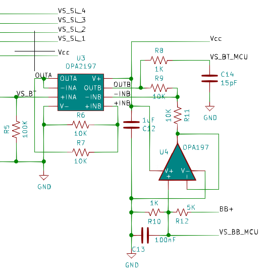
06/09/2022 at 21:20 • 0 commentsDuring early testing I discovered an oversight with the differential amp design. Its balance bus reference, which also serves as the sense input to the controller, did not have a buffer. This resulted in 30mV+ offsets in balance bus measurements, so I hacked in a buffer using another OPA197. U4 provides a low impedance drive for the differential amp and keeps the sense signal noise free.
![]()
As mentioned in the previous post this Balancer may at best be described as an awkward design because it requires a good deal of setup for the specific stack and management from the controller during operation. I believe that most balancers for the type of battery stacks this design is intended for achieve balancing thru transformer action: each battery has some form of transformer based converter (e.g. forward) with a winding ratio equal to that of the stack. That is, the primary is connected to the full stack, say 4x12=48V, and the secondary to the battery. This design can run continuously, and the current delivered to each battery can be monitored, instead of voltage, to establish health.
So, here's my run-down of problems with this design.
- Battery safety management is especially important with this design due to the use of unregulated flybacks. The prior log, Balancer Complete, described the protection circuits. The Battery Management Systems (BMS) in LFPs, particularly cheaper ones, tend to open inconsistently at both the fully charged & discharged ends. The balancer must respond quickly to prevent damage.
- The balance bus battery is a necessary complication in this design. It provides the bulk charge to augment transfers between batteries because the intrinsic transfer efficiency is poor (~77%). Hence, it is constantly in a state of discharge which requires transfers from batteries in the stack, which in turn unbalances the batteries. So the balancer plays a perpetual game of musical charge which, depending on the capacity (Ah) of the stack, reduces run-time. This could be addressed by making charge transfers asymmetrical (pull more charge out of high battery, push less into low). Ideally the balance bus battery is eliminated by powering the bias supplies from the stack; but the balancer would not work since the balancer side of the flybacks are powered from it.
- While this design demonstrates the ability to combine battery voltage measurements with a simple charge transfer mechanism, better data acquisition hardware is required. The balancer has demonstrated that it can measure reliably to about 50mV of resolution, but this is a relative measurement to other batteries in the stack and not absolute voltage. The main problem lies with the resolution and speed of the ADC and lack of any summing / integration capability.
- Even with better data acquisition, the intrinsic design has two additional challenges:
- Battery voltage settling time. Determining charge state by voltage alone is notoriously difficult. Accurate State Of Charge (SOC) requires that the battery be idle for up to 30 minutes: impractical. The balancer is polling batteries every minute. A battery that received charge a minute ago will reflect a higher voltage than its true SOC.
- Measuring batteries with a time varying load, such as an inverter, will give false results. This effect is magnified if the battery stack is small (lower Ah capacity) relative to the load. This happens because batteries are measure sequentially. In the current design the delay between measurements is 2~4mS: 4mS is approximately one quarter of a 60Hz sine wave. Faster acquisition hardware can eliminate most, but not all of this. Alternatively, multiple ADCs could be employed at the expense of considerably higher cost & complexity.
- The requirement to use timed transfers makes the configuration for a particular stack & balance bus battery combo time consuming. It must be done largely by trial & error; even rule of thumb math isn't of much help because the relationship between battery voltage & SOC is non-linear. I guess you could say that one small advantage of this design is that it can scale to stacks of different voltages without changing the individual balancer sections.
Experience
The litmus test for anything is "Would you recommend it?" Sadly, I'd have to answer with a resounding no. That's not to say I'm sorry I built it: I have gained invaluable experience and I've added some useful stuff to my tool belt. And, in spite of its shortcomings, it has proven to be remarkably hardy. I've done some pretty stupid things with it, and aside from a blown fuse or two it hasn't skipped a beat. -
Balancer Complete
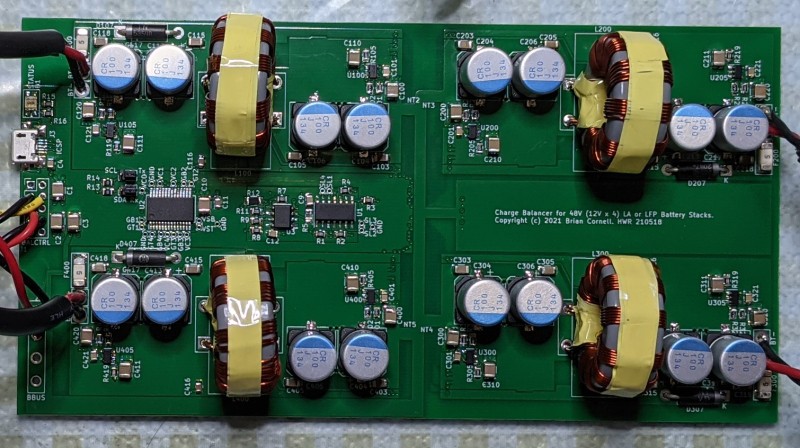
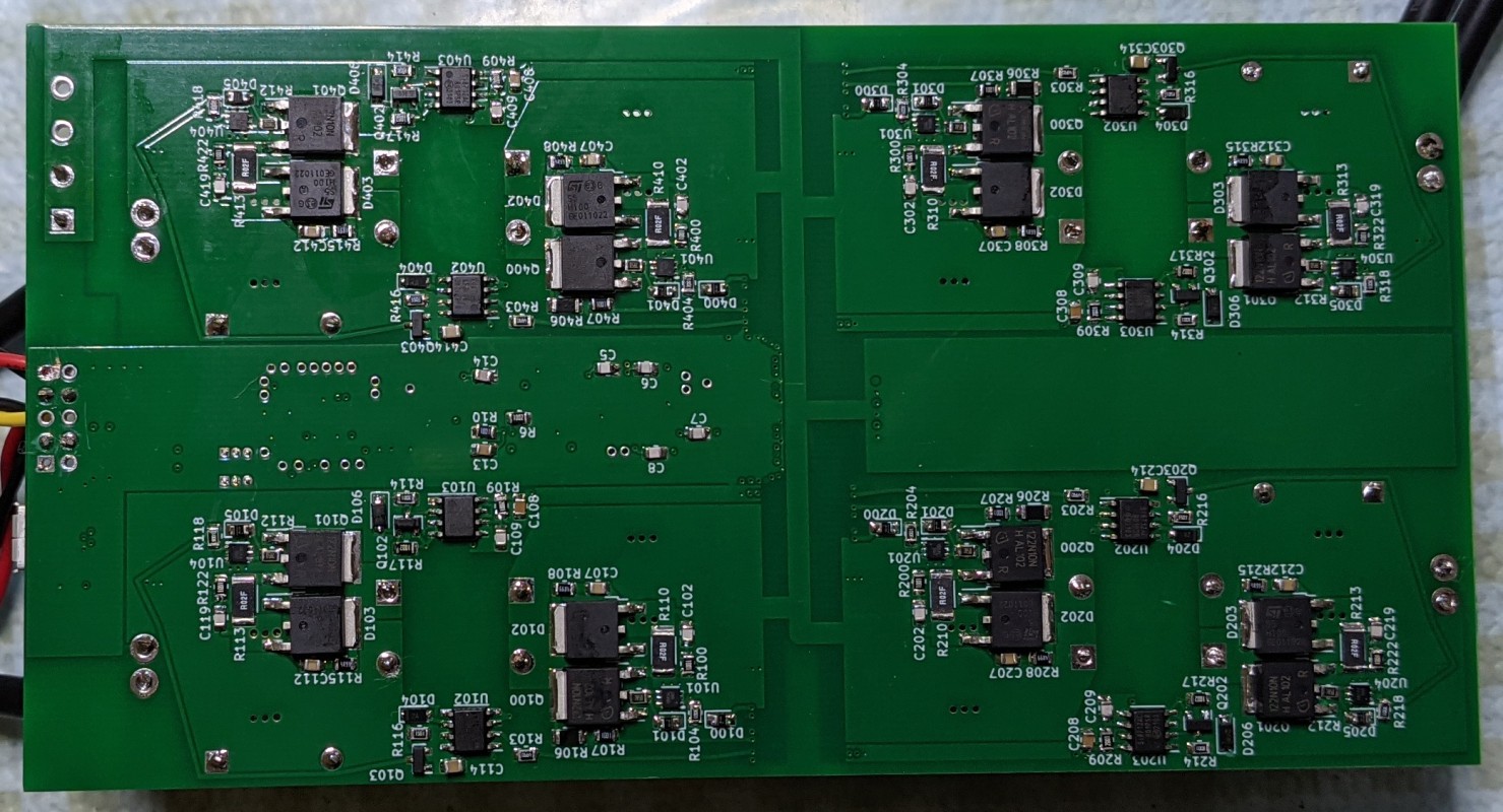
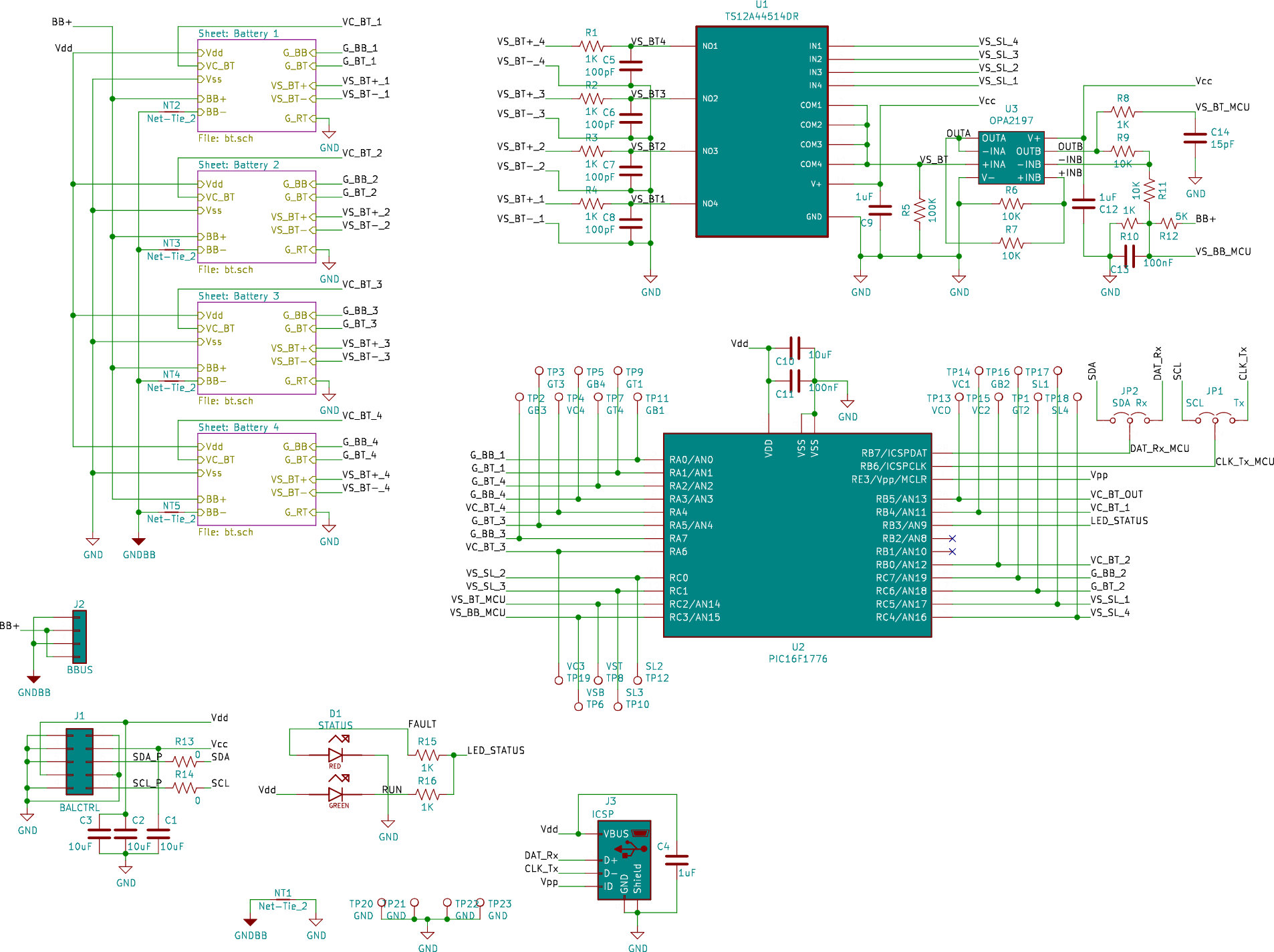
05/23/2022 at 17:49 • 0 commentsThe Battery Balancer is the final module to complete the PV->Battery charger design. It adheres to the original proof of concept and uses individual, bidirectional flybacks, to both transfer charge and measure battery voltage.
![]()
![]()
Specifications:
- Battery stack size: 12V x 4 = 48V (nominal, range 40V ~ 56V)
- Battery chemistries: Lead Acid (LA), Lithium Iron Phosphate (LFP)
- Architecture: per-battery bidirectional flybacks
- Operating frequency: 100kHz
- Voltage sense: via flyback voltage impressed on coupled winding
- Balancing method: timed direct transfer between highest & lowest batteries in stack
- Balancing resolution: 50mV
- Balancing current: ~1.5A (18W)
- Charge transfer efficiency: 77%
- Bias supply: +12V, +5V (provided by charger)
- Operating temperature: -20 - +50C
- Cooling: natural convection
- Calibration data and configurable operating parameters are stored in NVM
It integrates with the Charging module back plane for bias power and console access & control via 400kHz I2C.
Results are mixed. It does work as designed but in practice the combination of methodology and hardware selection is problematic. This is detailed in a subsequent log discussing performance & problems.
THEORY OF OPERATION
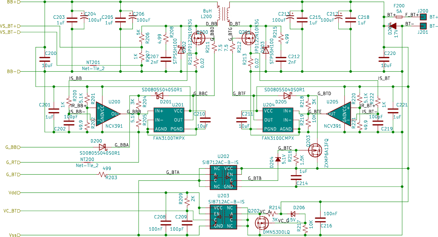
The Balancer consists of four identical bidirectional flyback sections, one per battery. The flyback inductor uses a 1:1 bifilar wound coupled winding that isolates the balancer from each battery and the common mode voltage of the stack. The balancer side of the flybacks connect to the balance bus which facilitates charge transfer between the batteries. It also connects the balance bus battery which powers the bias supplies and serves as a charge transfer buffer.![]()
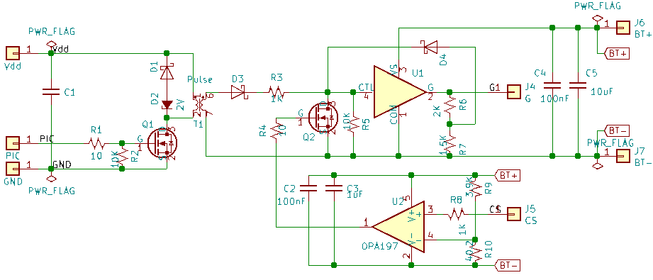
Each side of the flyback contains a low-side gate drive with the battery side employing an isolator for the gate drive signal. The gate drivers employ positive feedback via a schottky diode across the output/input to maintain the gate drive after a short (500nS) pulse from the controller to initiate the period.
The flyback control loop is 'constant on time': a low-side current sense resistor provides a voltage proportional to the inductor current ramp and is sampled by a comparator that terminates the duty cycle. The comparator's voltage reference is connected to the same supply as the flyback (e.g. either the battery or balance bus) which makes the flyback on-time ratiometric to the supply voltage and keeps power delivery consistent over a range of voltages. A schottky diode conducts the free-wheeling current.
This design is simple and rugged but must have a low impedance load (e.g. battery) connected to the output to avoid self-destruction. Since this cannot be assumed a protection circuit applies a logic high signal to the controller whenever the battery voltage is outside of safe limits (this is defined as a 'voltage condition' event). This signal is routed to the controller COG peripheral which terminates the gate drive without firmware intervention. The combination of bulk capacitance and a zener diode across the battery shunts excess energy for the few cycles required for the gate drive to terminate. In the event of controller failure the zener diode acts as a shunt to open the fuse and disconnect the battery. The controller incorporates a similar protection feature using a comparator, but this version of the design does not incorporate external shunt protection.
The battery voltage condition signals are OR'd, and the resulting logic signal is inverted and routed to the charger's controller via a dedicated pin. This allows the charger to immediately stop charging the stack. All of this occurs independent of I2C communication and without firmware intervention. Note that the balance bus voltage condition is not routed to the charger since it offers no additional protection or safety.
The Balance Bus flyback circuits contains precision voltage dividers that are used to sense the voltage impressed upon the gate drive during the battery flyback charge cycle. This voltage is the sum of the balance bus and battery voltage, (minus errors in inductor coupling, switch & current sense losses, etc.) and is routed to the controller section for measurement of the battery voltage.
An analog switch functions as a multiplexer to route the selected sense signal to a buffer & differential applifier. The differential amp subtracts the balance bus voltage and the controller's ADC quantitizes this sampled signal at approximately the midpoint of the flyback signal. Several samples are recorded & processed to derive the battery's voltage. This is more fully explained in the firmware code documentation.
![]()
The controller is a Microchip PIC 8-bit mid-range 16F1776 running at 4 MIPS that controls the balancer and communicates with either a console via RS232 (stand-alone operation) or I2C connection to the charger (integrated operation). The operating mode is set by a compile option and on-board jumpers connect the common communication pins to either the micro-USB jack (RS232) or the I2C bus. A combination Red/Green LED indicates the Balancer's status: Green=normal, Red=fault. Some faults are treated as recoverable (e.g. the controller monitors for the condition to clear & resumes normal operation), and others require a power cycle or reboot.
The controller monitors the balance bus & battery stack voltages at regular intervals and when the difference between the highest & lowest batteries (or the balance bus battery becomes low) charge is transferred. Charge transfers run for specific, configurable, time intervals that are set based on the size of the batteries in use. Battery voltages are monitored during transfers to terminate if low/high safety limits are exceeded. Transfers always operate in pairs and 180 degrees out of phase: the flyback portion (discharge into the balance bus) of the high battery occurs during the charge portion of the low battery.
The controller uses NVM to record a number of operating statistics on the balancer's operation and each battery. These can be used to tune operation and identify a problematic battery. NVM is also used to store calibration constants and a variety of operating parameters. Refer to the firmware documentation for a detailed explanation of the controller's operation.
-
Charger Section Done!
08/02/2021 at 16:46 • 0 commentsThe charging section and basic backplane design are finally done. The SEPIC card went thru a few iterations to get ringing in the switch & rectifier under control. A tight PCB layout is critical which includes keeping the outbound & return power traces aligned. Interestingly, I tried a synchronous rectifier but the efficiency gains were negated by the excessive snubber losses: the gate charge exacerbated the main switch turn-off ring due to inductive layout parasitics between the coupled inductor / coupling capacitors and the synchronous switch. Reverting to a schottky rectifier allowed for a much tighter layout that eliminated most of the ring and allowed the use of a small snubber. Now the switch runs hotter than the rectifier - goes to show that simpler is often better.
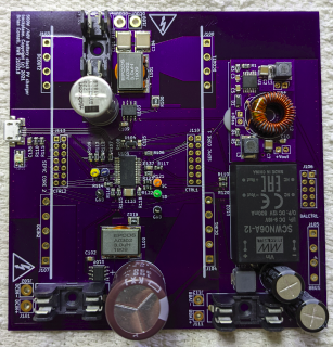
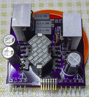
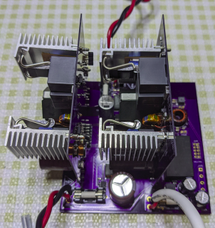
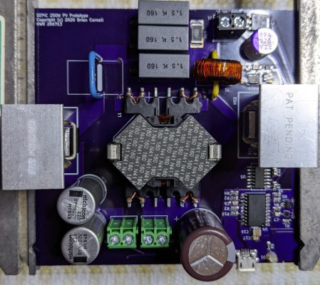
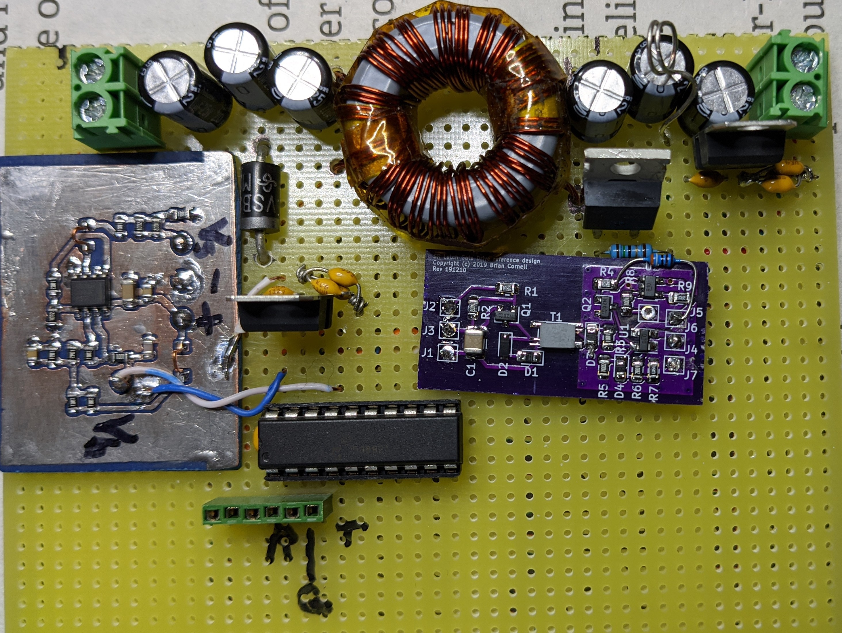
Here's the current build. The backplane contains the master controller for both SEPIC cards, +5V & +12V bias supplies, connections for PV (charger) in, battery stack (charger) out, and the balance bus battery.
![]()
Each SEPIC card mounts vertically via a set of soldered pins that provide mechanical support. The charger in/out sections include LC filters and hall effect current sensors to support MPPT and managing the stack's charge state.
![]()
![]()
Input Ripple Current
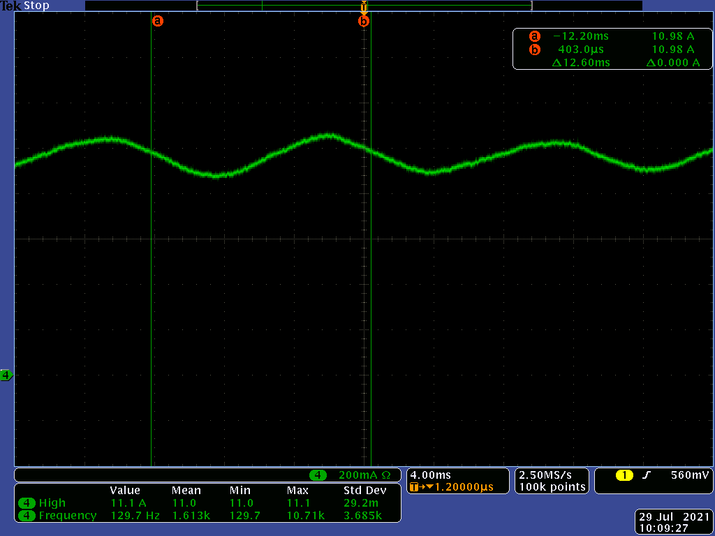
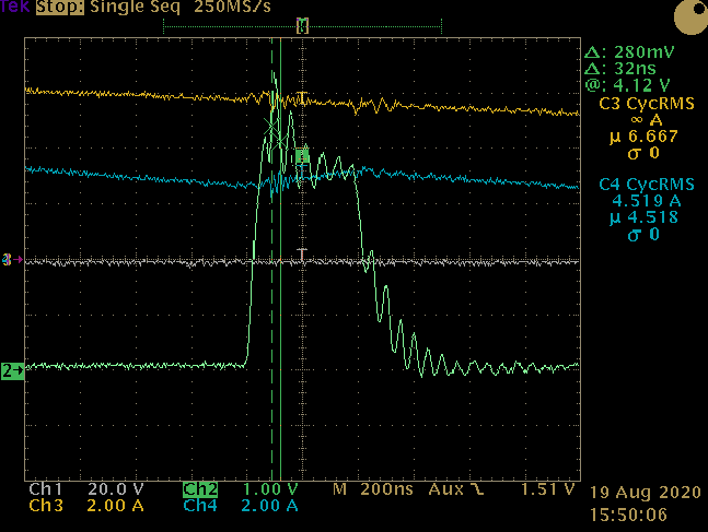
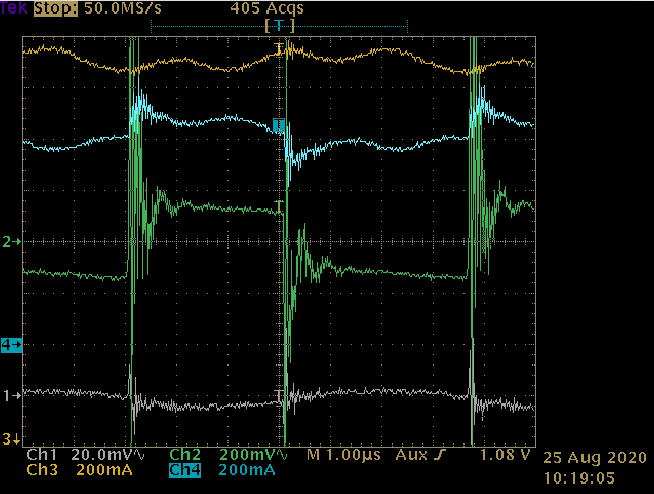
As discussed in prior logs, the SEPIC topology was selected in part due to the input current being continuous and the ability to 'steer' ripple current to the output with the use of a coupled inductor. The worst-case line & load condition is Vin=10V & Pout=90W. The trace below shows ~ 200mA P-P @ ~ 130Hz. Not bad.![]()
Efficiency
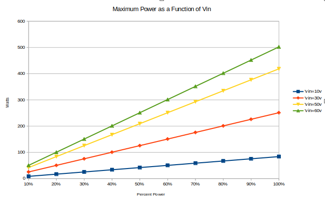
The design derates the charger's output as a function of Vin.![]()
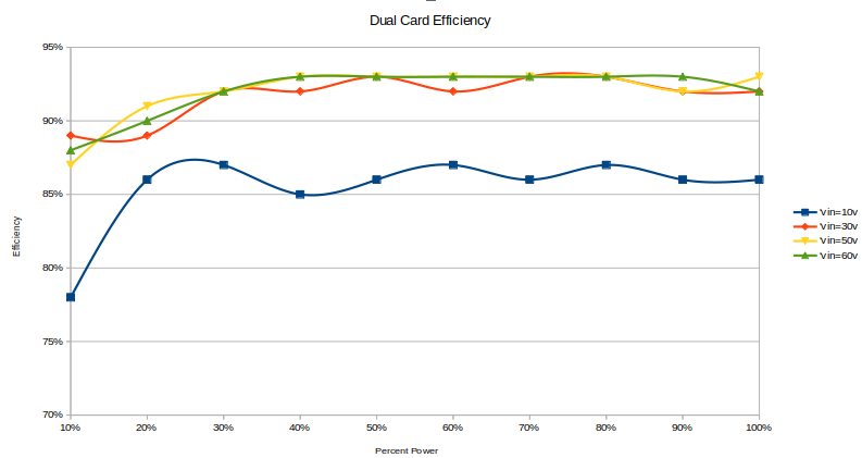
This maintains a relatively constant [maximum] input current to match the power curve of the PV array. Efficiency was measured with both cards operating at four input voltages. Minimum Vin, 10V, is the worst but at 30V & above the curves are surprisingly close with efficiency peaking at about 94%.
![]()
Next Up
The charge balancer section isn't ready yet but the backplane includes the necessary connections (right edge of backplane) for a development version. Once that's done the backplane will be redesigned to either support the balancer as a card or integrated. The SEPIC cards will undergo a final design revision to accommodate changes to the pin configuration on the backplane and to move temperature sensing from the rectifier to the switch.Thermal management will also drive the final layout. Natural convection was the original design goal (hence the vertical cards & heatsink fin orientation) but that is not realistic. Forced convection will likely dictate that the assembly rotate 90 degrees so that the SEPIC cards are horizontal and the fan can exhaust out the side of the enclosure.
-
Evaluating the SEPIC Prototype
08/29/2020 at 05:00 • 0 commentsOkay, I finally got this thing built and completed a preliminary evaluation. The Kicad, MPLAB projects, and updated design workbook are posted in the files section but don't rush to build it.
![]()
![]()
Specs:
- Input voltage: 10 - 80 volts
- Input current: nominal 4.3A @ 62V, full power
- Output voltage: 56V
- Output current: 4.5A (max)
- Maximum continuous power @ V_in > 60V: 250W
- Maximum continuous power @ V_in 10V: 45W
- Control mode: average current
- Bias supply: 12V
- Operating temperature: -20 - +50C (not validated)
- Design efficiency: 93%
Note that the power derates as the input voltage declines. This keeps the input current relatively constant and tracks with the maximum power available from the PV panels. Initial efficiency was closer to 90% but after improvements to the output diode, D2, it achieved 92% efficiency at 250W.
![]()
![]()
Overall, it worked as designed. The control loop is stable thru all operating regimes (with both external & internal ramps) and the coupled inductor / ripple current steering is solid. The coupling capacitor, C_ac, and associated snubber performed as expected with no resonance and within expected operating limits.
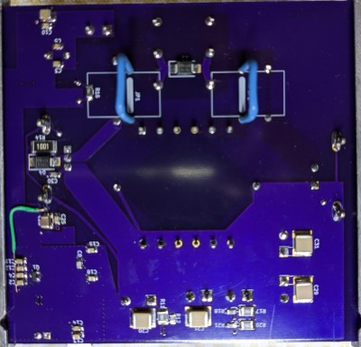
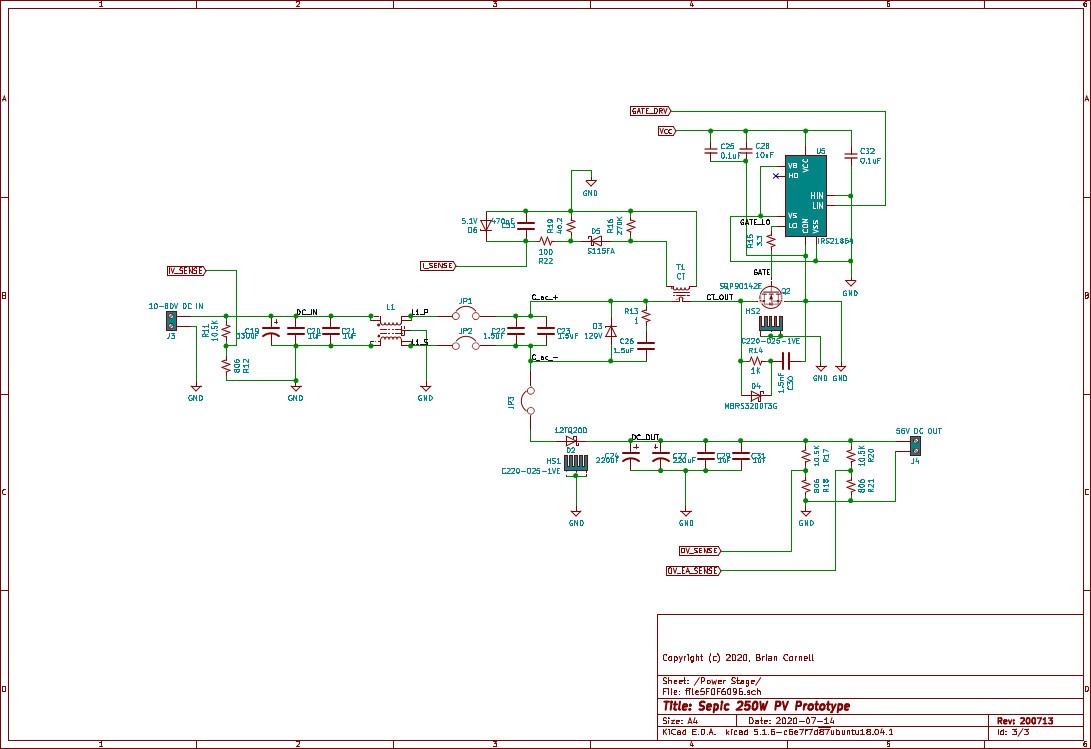
It does have some problems that are mostly the result of inattention because of my hyper-focus on SEPIC specific aspects of the design. The layout is also sub-optimal with several 'loop' jumpers to accommodate current probes at the expense of increased inductive parasitics.
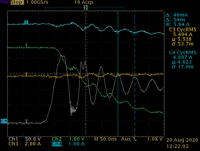
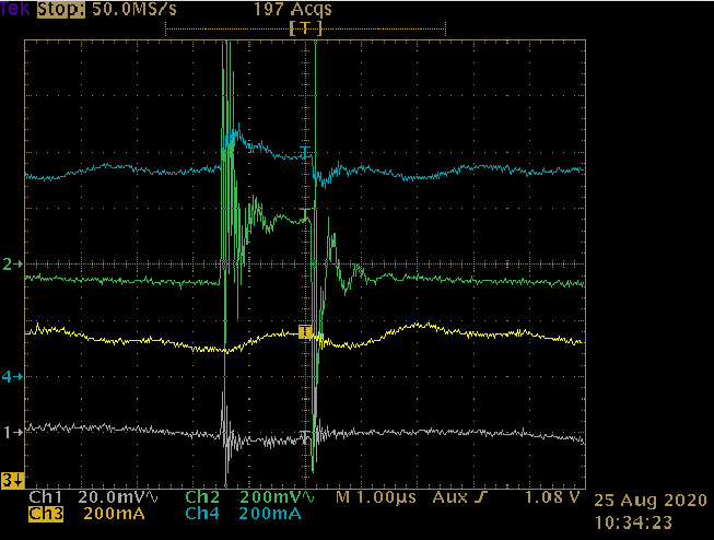
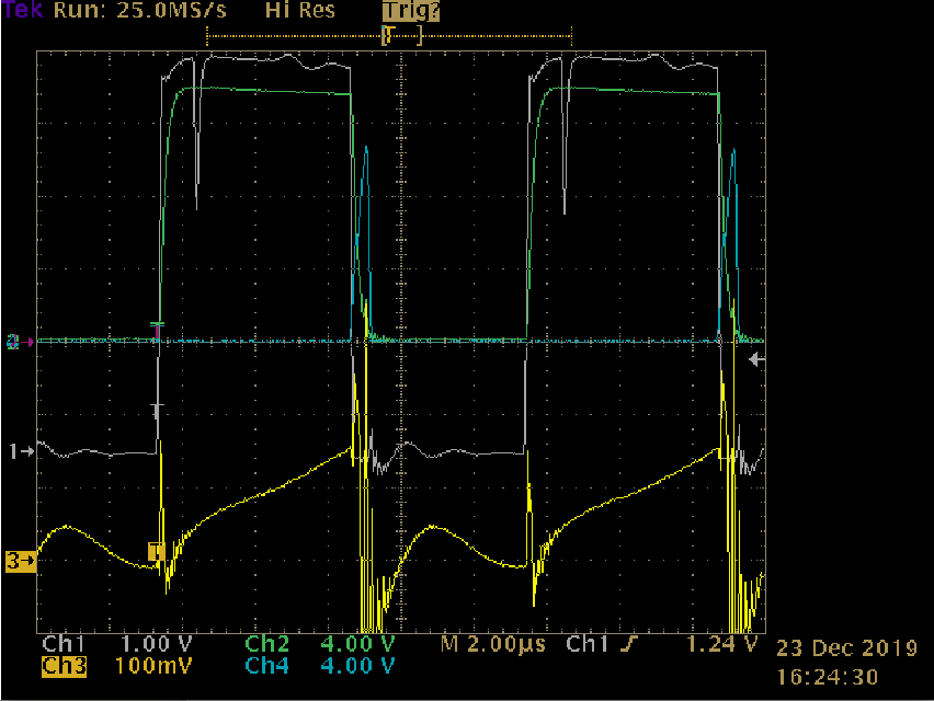
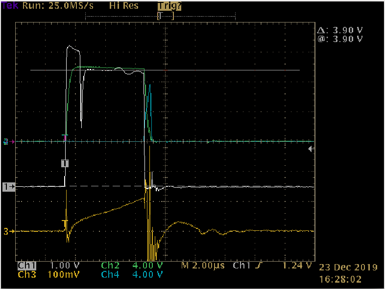
Switch snubber. The most serious is switch Q2 and its snubber. The root problem is the ring at turn-off. CH1=D-S volts, CH2=current sense (CT) circuit output, CH3=L1 primary current, CH4=L1 'secondary' (coupled) current.
![]()
The snubber does not fully dampen it but is still absorbing 3+W more than anticpated (for total ~ 4.5W). That, combined with inadequate Cu area on the PCB, sends the snubber resistor north of 200C in 30 seconds at full power. Since a proper fix would be difficult, and this wasn't the focus of the build, I decided not to fix and worked around (limited high-power run-times, forced-air cooling) during the evaluation.
Amazingly, Q2 did not avalanche/fail and ran close to predicted temperature. In an attempt to measure the non-dampened ring, I did remove the snubber but that resulted in the switch's immediate failure. The revised design will use a non-dissipative snubber that will probably send the recovered energy to the bias supply. To ensure robustness the revised design will use a different MOSFET with a higher D-S rating.
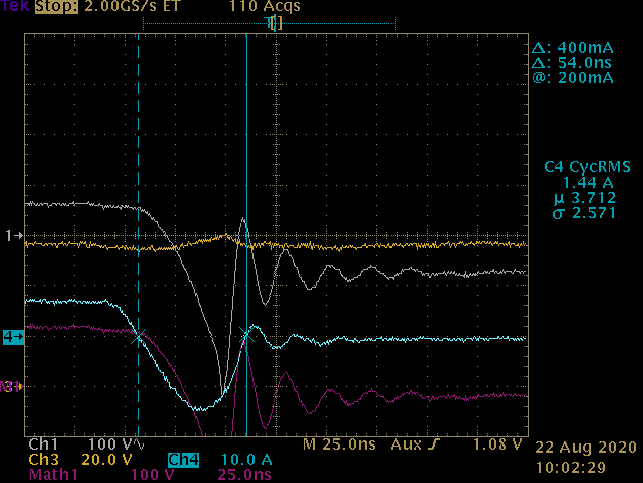
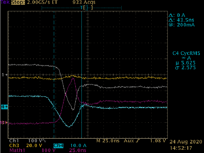
Output diode. The output diode, D2, had similar problems at the anode during turn-off because I hadn't included a snubber for it. CH1=voltage at anode referenced to ground, CH3=voltage at cathode referenced to ground, CH4=diode current, M1=CH3+CH1 (incorrect).
![]()
Its reverse voltage rating (200V) was being exceeded and it was avalanching - resulting in ~ 5W of additional losses (incredibly, albeit a Schottky, it did't fail). I fashioned an RC snubber which eliminated the ring except for the initial negative inductive swing but the high losses continued. I replaced the schottky with a 400V fast recovery diode (but higher forward voltage) and netted 4W. Interestingly, there is still a 10A excursion during recovery. M1 correctly shows the voltage across the diode and it is well within its V_r (CH3-CH1).
![]()
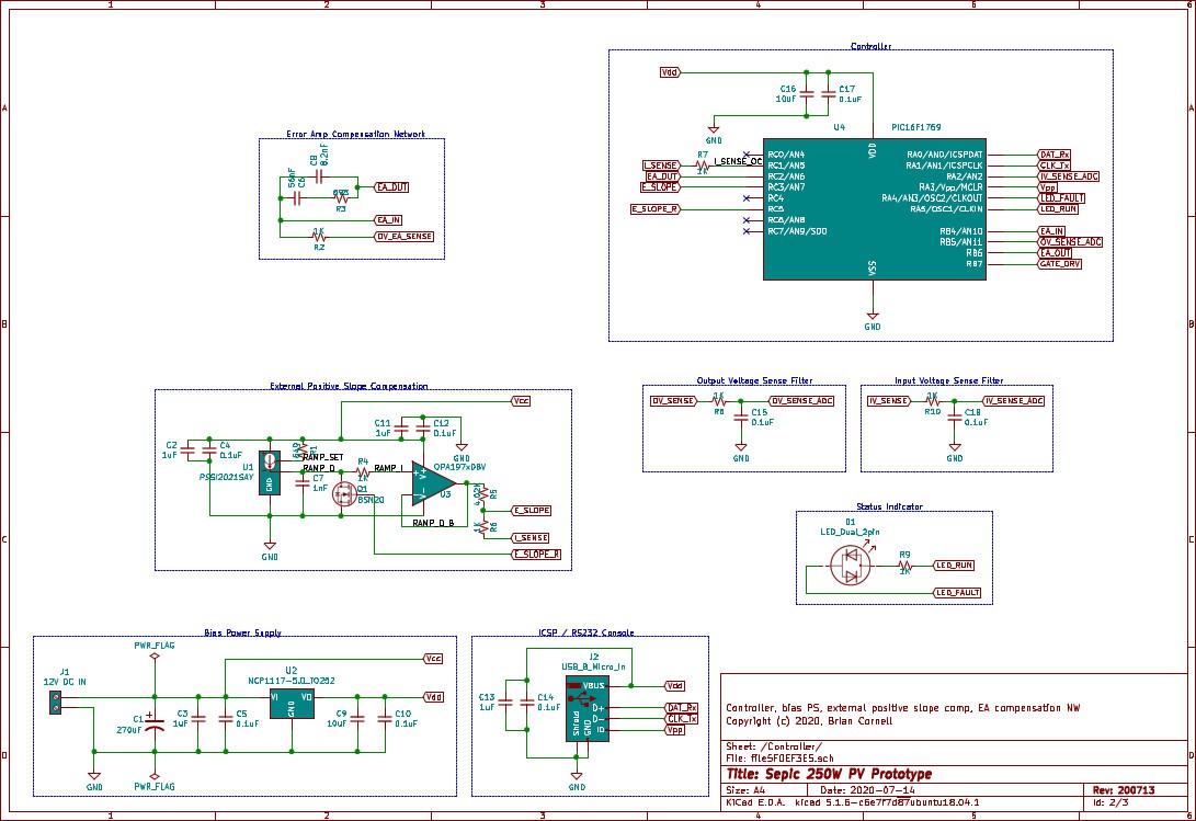
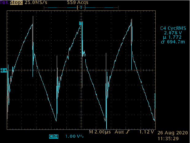
External slope. The external slope compensation circuit worked well but I made the mistake of powering it with Vdd (+5V) instead of Vcc (+12V). The problem with a 5V supply is that the slope becomes asymptotic above ~ 4.5V. Hacking the PCB to reconnect to Vcc and adjusting R1 for a ~ 1V/uS fixed the problem.
![]()
The external slope does have a ~ 500nS non-linear region at the start of the duty cycle due to propagation delays in the constant current source but this did not induce control problems at no/light-load conditions.
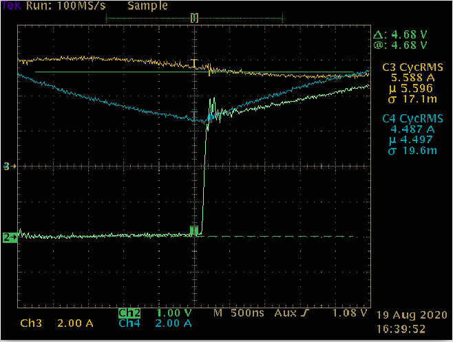
Current sense switching spikes. During initial evaluation the over-current protection would engage when loading at 250W with input voltages < 60V. A review of the current transformer circuit's output showed what I thought were noise spikes. These are uncharacteristic for a CT and I already had a low-pass filter on the output - which should have been my first hint.
![]()
I increased the value of C33 which, as it turns out, treated the symptom but not the problem. The locus was D2's reverse recovery current, so the CT was right! Channel two shows the 'corrected' leading edge of the sense signal.
![]()
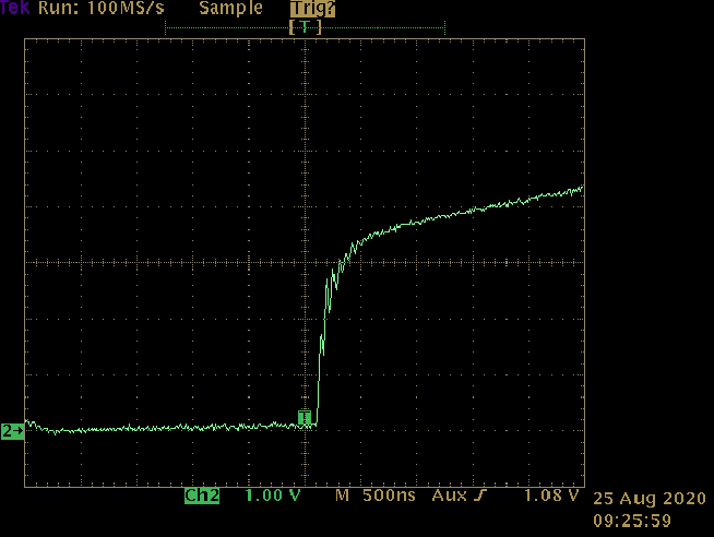
Still a bit of noise but not enough to cause problems. Same setup / trace after fixing D2:
![]()
All leading edge noise is gone; I should probably revert the low-pass filter cap, C33. The lesson here is to fully characterize before diving in to address specifc problems.
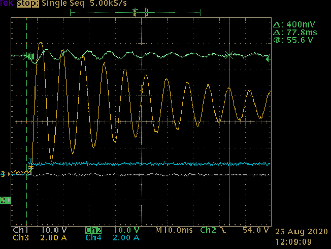
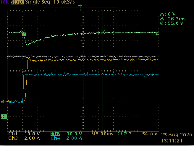
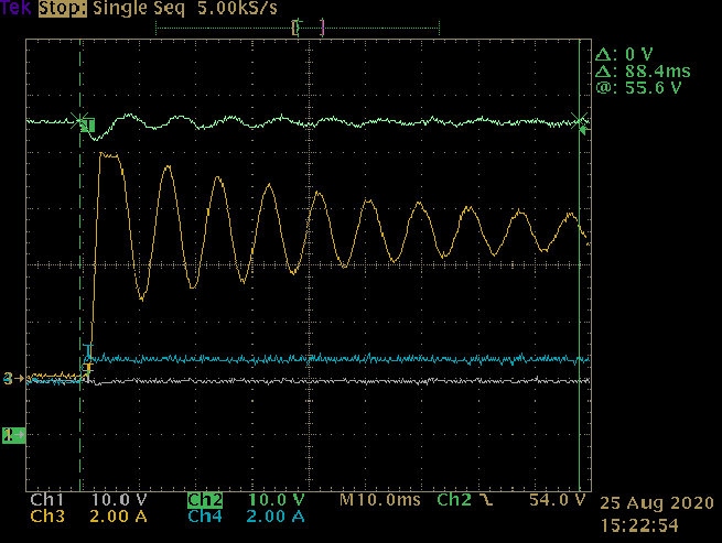
Control loop stability. I did not perform formal transient testing for a few reasons. First, the intended application, a battery charger, does not demand fast response. Second, the other testing done to the unit provided ample opportunity to observe instability: hot, excessive loading, start/stop at full loads, etc. Third, this specific design isn't going anywhere: its purpose is to qualify the SEPIC for the intended application and my design approach. That said, I did perform no->full load tests using an electronic load (HP 6063B) in constant current & resistance modes. The goal was to baseline the response and make sure that no gremlins were lurking.
The test regiment applied a constant full load to the unit while running with no load. The load is turned on & left on; not a pulse. Full load is defined as the maximum power the unit will deliver at the regulated output voltage for a given input voltage while running hot. An HP 6030A powered the unit with its current limit set to 9A to emulate the maximum current available from the PV array. Testing was performed in 10V increments from 10-60 volts using both the external and internal slope compensation ramps.
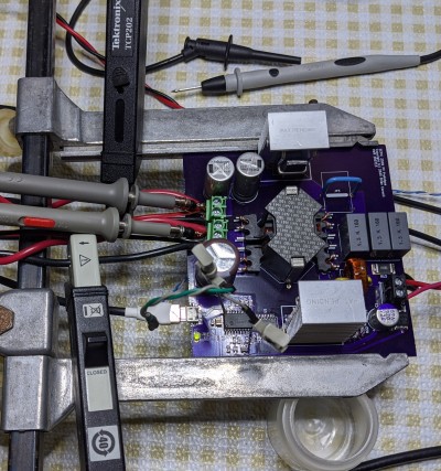
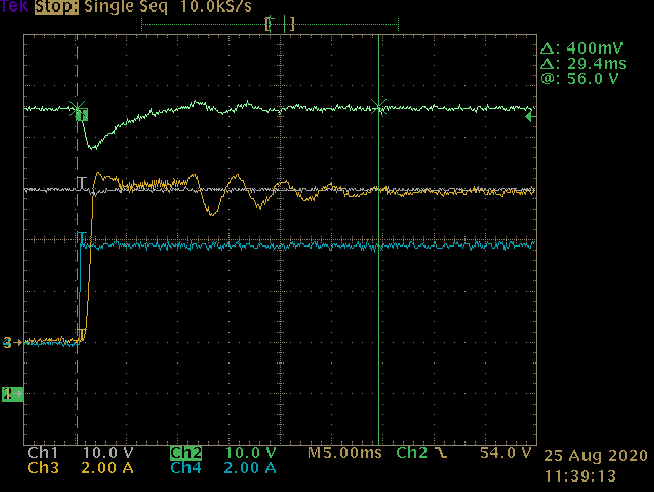
Channel setup: 1=V_in, 2=V_out, 3=I_in, 4=I_out. Channel 2 triggers on a declining output voltage. Passive 1x probes with soldered tip grounds were connected directly to the in/output terminals. Tek TCP202 current probes clamped to power leads as close to terminals as possible.
![]()
These traces are for 40V/3.8A and 10V/800mA respectively using the external ramp:
![]()
![]()
These are for 40V/3.6A and 10V/800mA using the internal ramp:
![]()
![]()
Looks like the external ramp's slope value (probably the compensation network too) could use some fine tuning. Predictably, the internal ramp's slope is a bit over-damped but eliminates all resonance except at 10V. The trade-off is that this eliminates some headroom that the external slope has to obtain higher power at lower input voltages. In spite of this the internal ramp delivers rated power across the operating spectrum for the application.
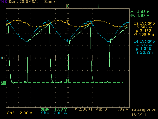
In/output voltage & current ripple. A key design parameter for this project is to minimize input current ripple because of the long lead lengths associated with PV installations. While the interleaved configuration of two SEPICs operating at 180 degrees with respect to each other should address this it was important to validate that ripple current steering worked as designed.
The channel setup is the same as for the control loop but the current channels are scaled to show the AC component. The TCP202 current probes & TDS784C don't allow AC coupling so the offset feature is used. This trace is for V_in=50V, I_in ~ 5.5A, and P_out=250W.
![]()
And this one is for V_in=20V, I_in > 7A, and P_OUT=125W.
![]()
In both cases input current ripple is less than 200mA RMS and voltage ripple less than 20mV. There is considerable switching noise on the output which is typical for a flyback topology including the SEPIC. Even with this the ripple current on the output is less than 200mA RMS.
Another way to view this is to examine the current wave forms of the coupled inductor.
![]()
This trace was taken while working on the CT problem. V_in=50V, P_out=250W. CH3=L1 primary, CH4=L1 coupled. While the primary winding's RMS current is higher it is a sinusoidal waveform with a smaller amplitude. Clearly, most of the ripple current has been shifted to the coupled winding which shows a significant AC component.
C_ac Ripple Voltage. I had a lot of concern that the ripple voltage across C_ac would exceed the manufacturer's spec and cause heating problems in the caps. Turns out the model was correct and the worst case ripple was as predicted. The trace below was taken with a Tek P5200 differential probe with V_in=62V, P_OUT=250W.
![]()
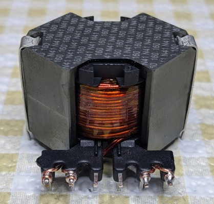
Coupled inductor. The as-built version matches the build spec in the previous log but does include an additional 1/2-turn on each winding since it terminates to opposite sides. This bumped up the primary inductance a bit but didn't materially effect performance.
![]()
Pin assignments:
- 11/12 - primary (+) in
- 1/2 - primary (-) out
- 7/8 - coupled (+) in
- 5/6 - coupled (-) out
Primary winding measured values:
- L=60.431uH
- L_l=5.6uH
- F_r=1.510MHz
- C_p=183pF
Secondary winding measured values:
- L=54.575uH
- L_l=5.139uH
- F_r=1.558MHz
- C_p=191pF
F_r is the resonant frequency and C_p is the calculated parasitic capacitance using F_r and L:
1 / ((2 * pi * F_r)^2 * L) (1)
Building it. I never intended to use this design for anything but validating the basics of the SEPIC and learning, so I wouldn't recommend building without the modifications discussed here. Even then there are thermal management issues, it lacks a proper bias supply & other circuit protection elements. The control firmware is a stripped-down refinement of my MPPTPROTO project that, like the hardware, contains no failure mode or protection limits.That said, it's a great starting point for a refined design. Be sure to follow proper safety practices since you'll be exposed to high voltages, currents, and temperatures.
Next steps. I'm going to prototype the 500W interleaved design and incorporate the improvements identified here. Part of this will be to confirm the controller that will be used in the final design (likely a PIC16F1776), gate driver, and whether it is worth exchanging the output diode for a synchronous drive. I really like the simplicity of a single low-side switch, and with the revisions made to this prototype the losses are acceptable.
Prototyping the full interleave setup will also allow me to properly evaluate thermal management and how this thing will be assembled (e.g. enclosure & environmentals): those are critical to decisions on layout, which impact thermal management, footprint, EMI, component selection, efficiency - pretty much everything.
Last but not least, the SEPIC is a fourth-order converter and I need to study the effects of interleaving two of them on the control loop & other stability issues. A single, outer, voltage control loop will connect to each converter's inner current control loop so, component tolerances & layout aside, output power should be balanced. But this too must be verified.
Parallel to this I'll start to flush-out the charge balancer and how it integrates with the charger section. Prototyping for the full stack will help drive most of the key decisions and help eliminate surprises.
Conceptually, I see the charger & balancer functioning somewhat independently with an I2C or SPI connection between them. The charger's controller would function as the master to collect data from the balancer (status, health, etc.) and to control when balancing can be done.
-
Completing the SEPIC Prototype Design
07/13/2020 at 23:21 • 0 commentsI ended my last post with mention of the snubber for C_ac to dampen the resonance with L_l. And, analysis & design of the control loop wasn't done. Completing the design resulted in further modifications and some corrections. An updated design workbook is posted along with a more complete LTspice model. This post addresses five areas:
- Current mode control and slope compensation
- Implementing leakage inductance
- Snubber for C_ac & L_l resonance
- C_ac AC ripple voltage ratings
- Control loop design
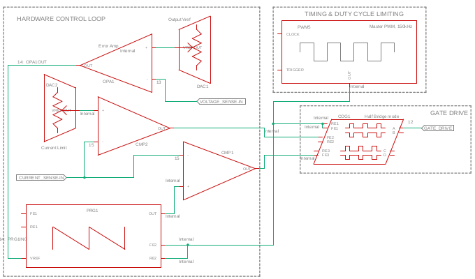
Current mode control and slope compensation. Current mode controls peak inductor current; not average and therefore requires slope compensation to prevent subharmonic instabilities. With a PIC MCU the ideal method is to use the Programmable Ramp Generator (PRG) to apply a negative ramp (M) that subtracts from the outer (voltage control) loop error amp signal. This compensated signal is compared to the switch current sense signal to control on-time. The diagram below depicts the peripheral configuration.
![]()
I prefer the use of current transformers whenever possible. They are efficient and require almost no conditioning to provide a clean sense signal. Their major limitations are space and reset time (volts-seconds product).
The value of M is in A/uS but uses the voltage analog of the current sense circuit. So with a sense of 400mv/A and a required M of 0.5A/uS the PRG's ramp would be 200mv/uS. Hence, the design of the sense circuit not only effects the power stage gain but also slope compensation. Other considerations:
- The PRG's minimum ramp is 200mV/uS: the derived M slope must be >=.
- The resolution (e.g. volts per amp) of the current sense circuit: a smaller V/A provides more dynamic range but a lower M value.
- Inductance: a lower L increases the charge/discharge slopes (M1/M2) but can exceed current sense circuit head room.
- CT reset voltage: a function of the volts-seconds product that is effected by the maximum current the CT must measure, on-time, and the V/A value derived from the burden resistor.
- Switching frequency: higher F_s reduces L and increases M at the expense of increased dissipation.
- Input ripple current allowance: setting a higher value reduces L and increaes M but will impact the CT design
- Changes to L or F_s effect the value of C_ac, the induced AC ripple, and L_l requirements of the inductor.
At an F_s of 100kHz I could not achieve an M of 200mV/uS without excessively high input ripple or loss of needed dynamic range in the sense circuit. 200kHz would have been perfect but the switching losses became excessive. 150kHz provided a workable compromise - just barely. So, I plan to include an alternate external positive ramp circuit that allows for smaller than 200mV/uS. For the prototype it can coexist on the PIC without conflict. The downside to this option is additional components and pin consumption. A small ramp can also be problematic due to a smaller S/N ratio that results in jitter in the output.
Implementing leakage inductance. Adding leakage inductance to the coupled inductor is highly dependent on the selected core, bobbin, winding placement, and methods. I have opted for a gapped RM core with a conventional bobbin (e.g. single winding area - not split, etc.) for size and availability from a mainstream supplier. This, along with winding by hand, limits the amount of leakage inductance obtainable: basically how many layers of tape you can place between the windings before running out of window area.
The higher operating frequency allowed for the use of an RM12 (vs. 14 for 100kHz). Testing of several builds showed that ~ 6uH of leakage was the limit (using the outer winding as 'primary' or L1 from the spice schematic). Interestingly, the outer winding always (across different test builds) measured several uH more (inductance) than the inner. I hypothesize this is due to the larger MLT and closer proximity to the core's outer legs which are not gapped.
An alternate way to implement L_l is as a physically separate inductor in front of L1 - which might make sense depending on C_ac sizing requirements. Ultimately I chose to work with the L_l I could obtain from the RM12 and size C_ac accordingly. When considering the snubber for C_ac this worked out quite well since the snubber's dissipation can be significant with small C_ac values (explained in next section).
Here's the numerical analysis of the inductor design. It specifies four strands - two are for each winding of N=18. Note that the winding losses aren't representative due to ripple current steering. The physical build is straightforward:
- L2 wound on bobbin first. Two strands of 22AWG (flat - not twisted) wound in two layers, 9 turns per layer. The layers are wound end-end with no fold-back between layers which makes winding & termination easier since both ends exit at the bottom of the bobbin. One layer of 3mil polyimide tape between each layer.
- Tape layer for L_l, N=25, 3mil polyimide.
- L1 wound on bobbin last. Two strands of 22AWG (flat - not twisted) wound in two layers, 9 turns per layer. The layers are wound end-end with no fold-back between layers. One layer of 3mil polyimide tape between each layer.
Snubber for C_ac & L_l resonance. The revised spice model demonstrates that resonance will occur during startup or a transient (run with & without the snubber). This resonance occurs because C_ac and L_l are coupled throughout the switching cycle. It not only injects EMI into the input supply but can degrade transient response. A snubber is necessary since the resonance is above the control loop's cutoff freqency (F_co).
C_ac & L_l can be treated as an LC filter and critically dampened according to the formula:
1 = R / sqrt(L_l / C_ac) (1)
Where R is the impedance of the damping network, in this case the snubber RC impedance at the resonant frequency. This will lead to a large value for the snubber capacitor, typically 2~4 times C_ac. In my design where C_ac = 3uF, that might require 12uF which is not practical. So I designed the snubber for an under-damped response for what I found to be acceptable in simulation. I expect to make adjustments based on in-circuit validation.
The snubber resistor's dissipation is proportional to the AC ripple voltage across C_ac: small C_ac values with large AC ripple components can induce significant power losses. For example, a C-_ac of 3uF results in a snubber R dissipation of ~ 1W. Halving its value increases dissipation to ~ 3.5W.
C_ac AC ripple voltage ratings. I spent a lot of time fretting over the maximum AC RMS voltage graphs when selecting C_ac (Metallized Polyester Film caps) and this imposed an additional constraint on the design. Calculated / simulation RMS currents were always well within limits. But, AC RMS voltage values were often out of spec or close. To ensure I had some margin I paralleled two and will evaluate the temperature rise in circuit. As a consolation I am able to use the same cap for both C_ac and the snubber.
Control loop design. An advantage of a coupled inductor SEPIC is that the power stage small signal model has a single pole response below the resonant frequency of C_ac & L_l. Further, since a snubber is implemented to dampen that resonance, the buck/boost transfer function can be used to plot gain & phase shift:
A = Ri / (Vramp_max – T_on * M) * [I_T - j * V_out / X_L1] (2)
Where:
A = circuit gain @ f,
Ri = Volts/Amp of current sense circuit,
Vramp_max = ramp voltage at start of switching period (e.g. max. output of voltage
EA),
T_on = switch on-time @ MPP,
M = compensation slope, V/uS,
I_T = I_in + I_outThe single pole gives a 90 degree phase shift. There is also a zero whose location varies based on load. For use in a PV design the lowest frequency is at MPP. The zero must be accounted for to ensure that there is adequate gain margin.
Because there is only a single pole & zero a type two error amp is used. A cross-over frequency, Fco, is selected along with frequencies for the EA zero & pole to allow suitable margin for Fco to occur with a -1 slope.
Wrap-up. The design workbook covers everything that's been discussed and shows how changing one parameter effects the rest of the design.
The LTspice model is representative of the intended power stage and was used to validate (sometimes with approximations) the design workbook. The control loop was not included and the behavioral logic components (U1, A1, A2) are used to emulate peak current limiting only (not current mode control). This was necessary to obtain the expected C_ac & L_l resonance behavior. Inductor L3 represents the leakage inductance of the coupled inductor (L1, L2).
-
SEPIC Design
03/09/2020 at 01:28 • 0 commentsBeing my first SEPIC design, I invested a lot of time reading up on their theory and design. Unlike the more mainstream topologies information is a bit fragmented, so it took a while to assemble what I considered a thorough design model. What I share here is a qualitative discussion that is by no means complete: I found it hard to succinctly describe the component relationships and key design considerations. The supporting mathematical (design) model can be found in the accompanying workbook.
The Limitations of the SEPIC. A machine doesn't need a lot of parts to be complicated, and SMPS demonstrate this well. Worse, a small component count simply means that each one possesses several critical parameters and that changing one cascades thru the entire design. And so it is for the SEPIC: the coupling capacitor and coupled inductor dictate the design.
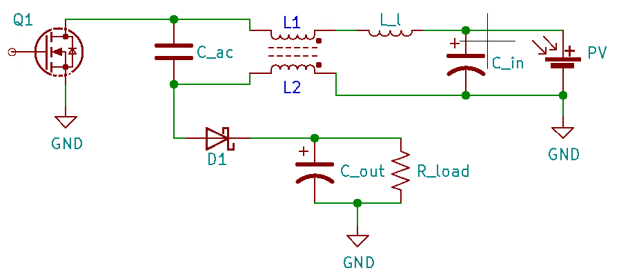
![]()
The SEPIC shines for its ability to transparently boost or buck the output voltage while maintaining a constant input current (with a ripple component). It performs best when the input voltage varies about the output by a range dictated by the current and voltage stresses imposed on the circuit elements.
The prototype for this project is spec'd to deliver 250W at 56V with an input of 63V. At 93% efficiency the input current is 4.3A. Skipping the math, the coupled inductor will see over 9A peak since each winding will carry over 4.3A. Add a 20% saturation margin and the inductor's saturation rating must be at least 10.8A. The coupling capacitor's RMS [ripple] current ratting, which is approximately equal to the input current, must be at least 4.3A. These are large values but not unrealistic.
But if this design is expected to deliver 250W with a 10V input, the inductor's saturation current rating would be 47A and the capacitor would require an RMS rating of 28A. Completely untenable.
The variable impedance of a PV system extends the operating regime of the SEPIC into this crazy territory since full power is only attainable at MPP. At 10V with the selected panel about 90W is available, but the supply will only need to deliver 45W (because the final design will interleave two supplies). This keeps the input current relatively constant at ~ 4.9A. Above MPP the current drops rapidly to zero so the design isn't much concerned about operation at higher voltages except tolerating the panel's open circuit voltage under no-load conditions.
The Coupling Capacitor. The coupling capacitor facilitates the unique boost/buck property of the converter. This is because L1 is isolated from the output making duty cycle the sole determinant of output voltage just like the buck/boost topology. But it is also its Achilles heel. Half of the energy delivered to the output flows thru it. This rectangular current waveform creates a high RMS ripple current thru C_ac. Depending on the operating voltages and value selected for C_ac, the ripple voltage adds additional stress. All of this imposes limitations on the type of capacitor that can be used and directly effects cost, size, and reliability.
A small C_ac value requires less board space and generally costs less, but lower values have higher AC ripple and as will be shown later can effect the inductor design and EMI footprint. The polarity across C_ac can also reverse when small values are used, and occurs when the ripple component exceeds the input voltage at maximum load. Non-polarized types are most often used, but polarized variants may be a better choice in higher voltage & ripple current applications.
SEPICs operating at higher voltages and RMS currents limit the type of capacitor that may be used and will likely increase the size & cost of the design. In low voltage designs MLCCs are the obvious choice because of the large capacitance available in small, cheap, low-inductance packages. The problem with MLCCs is their temperature & voltage derating. C0G/NG0 aren't available in voltages much above 50V with values of a few hundred nanofarads. X7Rs are the next best thing but their capacitance drops precipitously as the applied voltage approaches the rated value. Sure, they can be paralleled for higher values & compensation but are still limited to relatively low (<50) operating voltages. Last, their failure mode is a short which connects the input directly to the output.
Film capacitors are a good option for higher voltage designs. They check most boxes: stable temperature & voltage coefficients, low ESR, high operating voltages, wide selection of appropriate values, high reliability, and fail open. The trade-off is size, cost, and some parasitic inductance due to their large package sizes and thru-hole mounting.
Polymer electrolytic capacitors are an alternative in applications where a film cap is being considered. You might be able to get more capacitance in less space for the same or lower cost. They're available with (relatively) low ESR and decent ripple current ratings. Of course, maintaining the polarity across the capacitor by a safe margin becomes important.
Tantalum capacitors can also be used but I stay away from them. They are temperamental and can fail explosively when any of their parameters are exceeded.
The Coupled Inductor. It is possible to consolidate the individual inductors because the windings maintain the same polarity and voltage at all times. The coupled inductor halves the inductance requirement because it must support twice the current. Even though the coupled inductor may be larger, the overall footprint is reduced.
Using a coupled inductor subtly modifies the SEPIC's behavior. The rectangular current thru C_ac resulting from the switching cycle induces an AC ripple voltage across the inductor inversely proportional to C_ac's value. This generates an additional circulating current across both windings of the inductor that distorts the triangular input current ripple waveform, increases EMI, and creates stability problems for the control loop. This problem can be overcome by deliberately introducing leakage inductance to reduce this circulating current.
The Enmeshed Relationship of the Coupled Capacitor & Inductor. The design starts with selecting a value for the coupled inductor, and this is most easily done by establishing a limit on the input ripple current. This limit is usually set as a percent of the input current at maximum load. High input ripple creates more EMI but allows for a smaller inductance and maybe a smaller core. The reverse is also true.
The values for L, L_l, and C_ac are interrelated: a small C_ac value will generate a larger ripple voltage and require a larger leakage inductance to oppose it. L's value influences L_l and C_ac because the smaller the inductor's ripple (e.g. magnetizing) current, the larger the product of L_l & C_ac must be to compensate. This is because C_ac's circulating current must be reduced to a value less than L's input ripple to minimize the distortion.
To summarize, the values for C_ac and L_l are inversely related and the product of C_ac and L_l are directly related to L.
Once a value is chosen for L, the value for C_ac is set. Its value should be as small as possible to minimize cost & space, plus smaller values also offer a wider selection in voltage range and tighter tolerances. But not so small that the required L_l isn't possible (it is not a separate inductor as shown in the schematic).
There are two approaches to establishing the leakage inductance value: by selecting a target input ripple current or setting the circulating current induced by C_ac equal to the magnetizing inductance. The former uses L_l to shift (or steer) input ripple to L2. I have chosen the latter approach since the interleaved design eliminates input ripple as a concern.
Obtaining a specific leakage inductance is dependent on the core type, winding placement, and configuration. With a toroid you can get a lot of leakage inductance by placing each winding on one half of the core. They are my default since they are usually easier to wind, but for this design I'd need a large & expensive core. Instead I went with a gapped RM14. L2 (secondary) is wound first. Leakage inductance is obtained with several layers of insulation (3mil polyimide) wound on top of it and then the winding for L1.
A potential problem with the introduction of L_l is resonance with C_ac. The frequency will likely be well above the control loop's gain and can wreak havoc. An RC dissipative snubber can fix but I haven't decided on this approach yet (but I will probably accommodate on the PCB).
SWITCHING COMPONENTS
In an earlier post I had suggested using a synchronous switch for D1, but after looking at the dissipation and added complexity of a high-side drive it isn't worth it. Q1 and D1 see roughly the same peak currents, and a schottky diode incurs only 1W additional over Q1. So for the prototype I'll keep it simple and stick with a diode. -
SR Latch rev 2
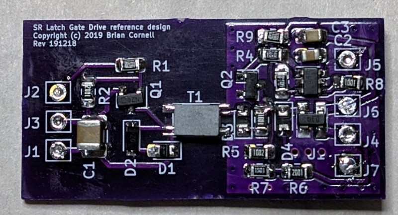
01/15/2020 at 22:25 • 0 commentsI finally got around to testing with the TI TLV1805 comparator. Basically the same circuit but I did rework the PCB for a tighter layout.
![]()
![]()
The TLV1805's performance was disappointing. It's propagation delays were about the same as the MIC6270 - about 1uS. Aside from a cleaner (square) output due to the push-pull driver, its performance (ratiometric, stability, etc.) was identical to the MIC.
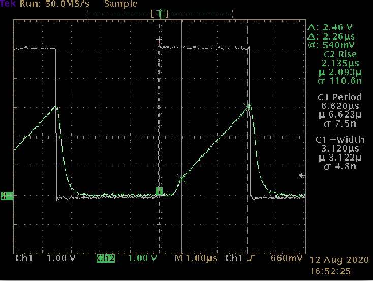
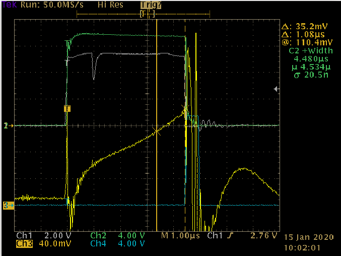
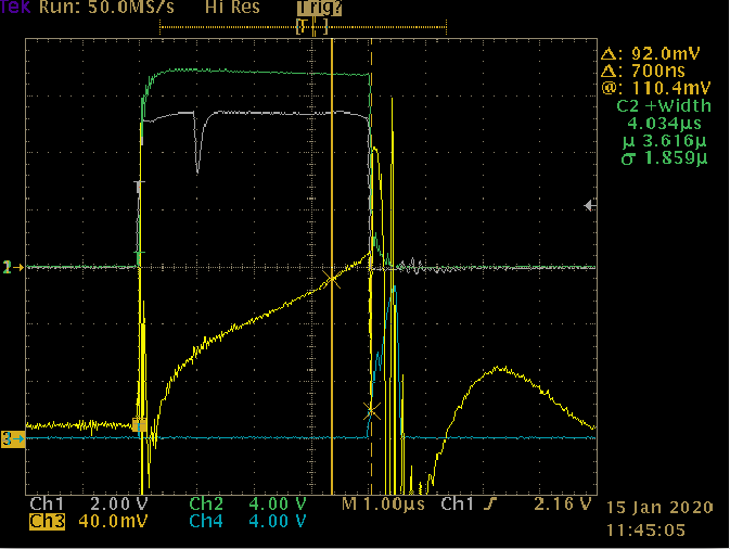
I decided to lower the Vref to 110mV which equates to 3.3uS, so with a 1uS delay I'd get a duty cycle under 4.5uS. I needed to make sure the timing would track linearly to the reference since going much lower becomes a problem for stability in noisy environments. The duty cycle dropped to just under 4.5uS - okay but not much margin if the design dictates a shorter on-time. Below is the timing trace - note the cursors marking Vref and turn-off time.
![]()
This outcome forced a reevaluation of the MIC version: I updated Vref to 110mV and repeated the timing tests. It bested the TLV by nearly 400nS for a duty cycle just over 4uS:
![]()
CH1=gate drive input, CH2=gate drive output, CH3=current sense input @ comparator, CH4=comparator output. Aside from the TLV's clean output pulse (hard to see), the traces are identical sans the shorter DC of the MIC.
The MIC's output has more slew because of the open-collector output stage and pull-up resistor but it does not effect performance. Given this, the MIC6270 is the obvious choice. The only points against it are the need for a pull-up resistor and temperature qualification to ambients of 85C (vs. 150C for the TLV). Temperature should be okay since thermal management will keep the maximum rise under 30C with a maximum ambient of 40C. So, with a unit costs on Digikey of $0.33 plus a $0.10 resistor I can buy two of these for less than the unit cost of a TLV1805. Sometimes the cheaper part really is the better choice.
While I was wise to test both versions, I could have been smarter and known the TLV1805's performance if I had studied the data sheet more closely - as it applies to this application. In this case it is the combination of hysteresis and overdrive. The TLV has 14mV of hysteresis intentionally built-in to prevent false triggering. Assuming Vref is centered in the hysteresis, 7mV equates 200nS:
Given (V * dt) / L = di
and I * R = V, the current sense voltage increase by
((V * dt) / L) * R,
substituting ((14 * 200e-9) / 8.35e-6) * 0.02) = 6.7mV
Figure 47 shows the propagation times based on the overdrive (the instantaneous difference between the comparator's inputs) with a 12V supply. At 25C it's ~ 800nS. This plus the hysteresis time delay is about 1uS.
Conversely, the MIC6270 does not have the hysteresis feature and its propagation times are solely based on overdrive. A 20mV overdrive will produce a 5V high output in about 500nS which is close to observed performance.
Okay, the MIC it is. Now I can start work on a complete draft of the balancer section and prototyping the SEPIC for the charger.
-
CHARGER DESIGN & TOPOLOGY SELECTION
01/06/2020 at 02:16 • 0 commentsIn between work on the balancer I've been considering topologies for the charger. So much depends on the panel configuration and working voltage. Within the charger, higher voltages correlate with higher efficiencies because of lower currents. This is even more important with a homebrew design where heavy-weight PCB costs are prohibitive and inductor / transformer fabrication capabilities are limited.
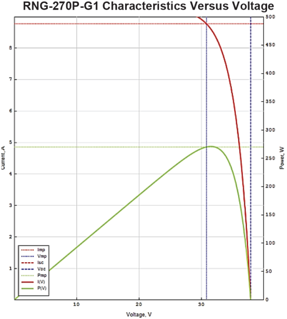
The TS350 project provided many lessons on the limits of power, efficiency, and transformer design with low input voltages that I want to avoid repeating. I settled on 500 watts with a nominal 60-65V input. Two 270W, 31.4V, panels in series would power the charger and deliver 540W at peak MPP. Of course these are perfect condition numbers that will [likely] never be obtained. Further, it requires the charger to have a minimum 92.6% efficiency (500/540). With an input current of 8.6 amps RMS this could prove challenging.
Here's the I-V curve for the panel I'm considering. A lot of energy is left on the table if the charger isn't able to boost the panel voltage to that of the stack.
![]()
Even at 10 volts there's better than 90W available. With two panels in series there will be 180W @ 20V. So I need a topology that can handle open circuit voltages in excess of 80V and capable of boost to at least 20V and preferably 10V.
Another key criteria I have is to minimize input current ripple since the panels will probably be located several meters away from the charger and high frequency ripple generates copious EMI and increased losses in the supply wiring. For example, a pair of 10AWG wire ten meters in length with 3mm lead spacing has ~ 3.36uH of inductance. To limit the voltage noise to 50mV with a ripple current of 1A would require 5,400uF of bulk capacitance. Output current ripple isn't as much of a concern since the charger will be located close to the battery stack and they are essentially a very large super capacitor.
Last, I prefer the power stage to be as simple as possible: defined by a minimum of switching and inductive elements since these incur most of the efficiency loss.
So far the design criteria are:- Output voltage=56V
- Output power=500W
- Output current=9A
- Efficiency=92.6%
- Nominal input voltage=63V
- Maximum input voltage=90V
- Minimum input voltage=10V
- Maximum input current=10A RMS
- Input current ripple <200mA RMS
- Simplified power section
- Isolated output not required (the battery system must be on earth ground with the panels)
As a rule I try to avoid center-tap windings on transformers. First, they are inefficient: each half winding is only active for a half cycle. Second, they waste valuable winding area and, depending on the number of turns & windings, can require a larger core size than non-CT variants. Third, the parasitic winding capacitance leads to damaging ringing on higher voltage windings: the end-end voltage is 2x the voltage applied to the half winding. This is worse for windings with a large volts-per-turn ratio. Eliminating #3 requires equipment & skills that I don't possess.
Against that backdrop I considered traditional full & half-bridge topologies. They would probably work but either require center-tap transformers or full-bridge switching. The secondary voltages aren't particularly high, but the voltage difference from end-end of the secondary will be 120V and that is close to the threshold I have found for excessive ringing on my home-built transformers. Conversely, a full-bridge rectifier on a conventional secondary creates a lot of loss.
Then there are flybacks. A non-isolated flyback won't work because it can't regulate to a lower voltage. An Isolated flyback can, but even in continuous mode they generate significant input switching ripple because the input current is discontinuous.
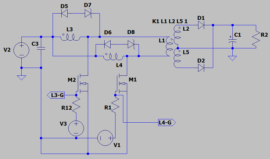
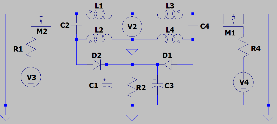
That sent me looking for something new. I stumbled on this current-fed full bridge topology in an ST reference design for a microinverter. It looks like a derivative of a Weinberg circuit although I can't find anything in the literature crediting it to that. In a conventional Weinberg flyback primary feeds the center tap of a push-pull transformer making it current fed. The flyback secondary can connect to either the input or output of the supply to reduce ripple current at that node.
![]()
This topology simplifies both the transformer and flyback design and, like the Weinberg, has only two switching elements and is a current fed design. It is quite elegant and has many advantages:
- Input current ripple cancelation because of 180 degree phase shift in switching
- Single winding for each inductor
- Single winding primary
- Single or center-tap secondary
- Eliminates staircase saturation of transformer core
- Only two active switches
Basic operation is simple but a bit different from most bridge configurations. Inductors L3 & L4 operate in continuous conduction and, M1 & M2 switch 180 degrees out of phase and must overlap which implies a minimum duty cycle of 50%. When M2 is on L3 is charging. M1 is off and L4 is discharging thru the transformer primary (L1) & M2. Towards the end of M2's on time (depending on DC), M1 will turn on. With both M1 & M2 on the voltage across all transformer windings goes to zero. Both inductors are now charging. M2 switches off under no voltage stress and L3 discharges thru L1 & M1. This continues and the cycle repeats.
Output voltage is determined by load, duty cycle, and the transformer turns ratio. It is by nature a boost topology: the voltage the inductors impose on L1 is determined by the volt-seconds balance and hence duty cycle.
The impedance of the input inductors make it a rather bullet-proof design. And, even though I would have to use a center tap secondary I thought I could make it work for the charger by setting a step-down ratio on the transformer. It modeled well in spice at nominal voltages but didn't do well at 20V and below. It also suffers at higher voltages because it must be run discontinuous which generates more current ripple and lower efficiencies. As much as I like it I had to abandon it for this application.
Initially I put the SEPIC in the flyback bucket but decided to take a closer look (glad I did).
![]()
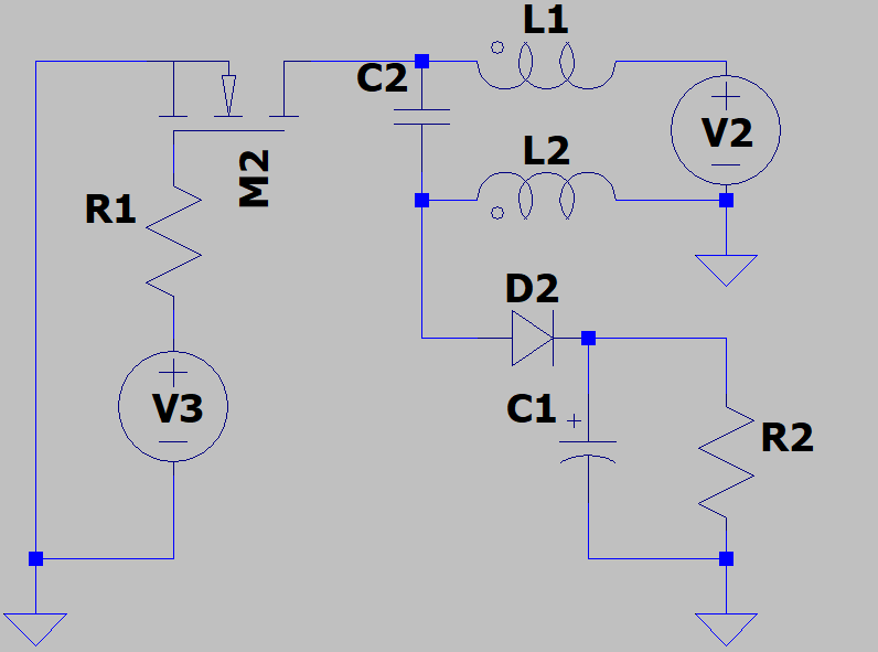
Like conventional flybacks it has only one switch - two if you replace D2 with a MOSFET for synchronous rectification. L1 & L2 can be wound on the same core and use the same number of turns which makes for a simple inductor build. Like the non-isolated flyback, L1 can run in continuous mode for a continuous input current. Best of all it can function as a buck as well as boost simply by varying duty cycle.
When the converter is first energized - before M2 begins switching - C2 charges to the input voltage (V2) thru D2 and the load (R2). When M2 turns on L1 begins charging. C2 charges L2 via M2 as well. This means voltage polarity will be negative with respect to the supply negative node but the current flow will be the same polarity as L1. While M2 is on the load is supported by C1 and there is no current flow thru D2. When M2 switches off both inductors reverse polarity by flyback action and deliver energy to C1 and the load. Energy from L1 & V2 must flow thru C2.
Since the SEPIC is still a flyback converter, the charger's power requirement will generate a significant ripple current unless the inductor value is made very large. Also, the ripple current of C2 will be larger than the output current since all energy transfer flows thru it. This is usually the limiting factor for SEPIC applications.
However, both problems can be solved by interleaving two converters that operate 180 degrees out of phase. Most input current ripple is eliminated because the triangular current ramp of each cancel. Since each converter only delivers half the power (250W), the peak currents thru C1 can be handled by paralleling MLCCs.
![]()
Spice simulations of the SEPIC interleave concept are promising. Full power efficiency at nominal voltage is 92.9%. D1 & D2 represent about 20W of losses and most of that can be eliminated with synchronous MOSFETs. At minimum input voltage (10V) the design delivers 90W at about 90% efficiency. Of course, this is spice and no real-world parasitics & components are modeled, but these results are promising enough to warrant prototyping.
My plan is to build a single 250W converter for evaluation. There are plenty of SEPIC controllers out there but I will use a microcontroller for better control over operation - particularly the control loop. SEPIC's have four poles in their transfer function which makes the loop harder to stabilize. And, I also have to contemplate how to balance the converters to ensure that each delivers 50% of the output.
-
SR Latch rev 1
12/30/2019 at 22:13 • 0 commentsThe pin pitch on the SOT-23 packages is too fine for my homebrew PCB abilities so I had it fabbed by Oshpark. It was also a good practice for using Kicad instead of Eagle.
Glad I did since Captain Obvious made the mistake of trying to use the OPA197 as a comparator. I did so for reduced component mix and because comparators with wide voltage supply ranges have have long propagation delays - greater than 1uS. But as anyone who knows op-amps will tell you they cannot be used as high-speed comparators, no matter how fast they are (GBW). With a large voltage delta, the inputs saturate and take several microseconds to desaturate. I measured propagation delays greater than five - totally unusable.
I found two comparators that might work. Microchip has a pin-compatible open-collector, wide supply range comparator (MIC6270) that's cheap but slow - on the order of 600nS-1.3uS. But I could evaluate it in the existing prototype circuit. TI has a push-pull (TLV1805) that costs the same as the OPA197 and is much faster - 400-600nS - but isn't pin compatible.
For both, the approach is to set a lower Vref to commence turn-off at a lower current which, when accounting for their propagation times over temperature, terminates the duty cycle appropriately. This works for normal operation but won't protect against dead shorts. However, this is an acceptable trade-off since the circuit will be fused and a short means something is broken anyway.
I was able to evaluate the MIC6270 immediately with just the addition of a pull-up resistor to the existing PCB. I did a new layout for the TI chip that's a bit more compact (and hopefully transferable to a complete design). I'm already leaning towards the TI comparator since it's faster and has a push-pull output stage that eliminates the resistor. I'll post a log when that evaluation is done.
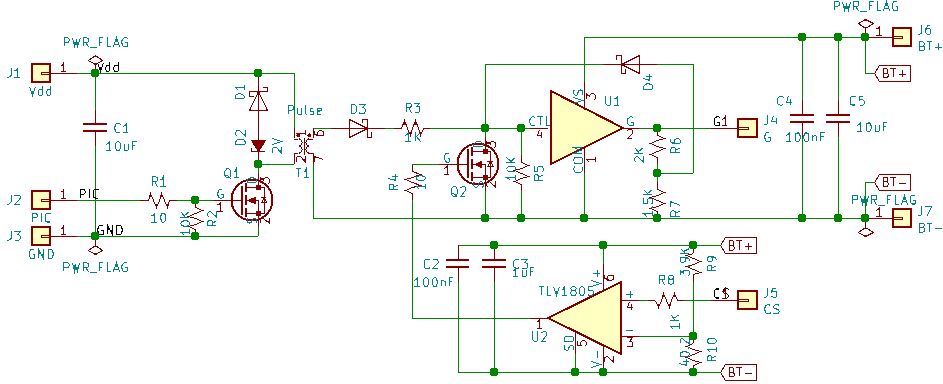
Here's the circuit that the OPA197 & MIC6270 were evaluated in.
![]()
![]()
They were fitted to the flyback prototype and replaced the conventional gate drive circuit. A 1uS drive pulse is issued by the PIC.
It did a bit better than expected. This trace was taken with a 14V supply emulating the battery. CH1 is the drive pulse seen by the gate driver's input, CH2 is the gate drive output, CH3 is the MOSFET source pin (e.g. current ramp), and CH4 is the comparator's output. At 14V the comparator should trigger at 140mV. There's about 800nS of delay.
![]()
Here's the same trace setup at 10.2V. Identical timing (ratiometric) as intended. Note the drop in the positive feedback as well as the droop at the end of the drive pulse. Below this voltage the driver would fail to latch because the voltage divider (R6/7) minus D4's forward voltage was less than the pulse drive input. The droop is due to the feedback loop's relatively high impedance. So a refinement is to select divider values that ensure latching across the intended operating voltage with sufficient noise margin. The bottom of the divider could be eliminated but the higher voltage adds time to the turn-off.
![]()
I spent some time characterizing at various voltages, running in sampling mode (10kHz) as well as charge transfer (100kHz) and its operation is stable. Voltage measurements are consistent with those taken using the standard gate drive. In a pinch this circuit would work but I'm betting the TI will do better.
Last, the gate driver and MOSFET are not matched; the MOSFET's gate charge is considerable since it's designed to switch 100A and I had to use a 10 ohm gate resistor to limit peak current for the driver. Not surprisingly, the gate driver's output trace (CH2) shows a rounded turn-on/off and there is considerable ring with more dissipation from the MOSFET than expected. Not a big deal since wasn't the focus of validation.
Solar Charger & Balancer for Lead Acid Stacks
Charger & Bidirectional Balancer for 48V Lead Acid Battery Stack
