-
A goal was achieved
02/07/2020 at 10:57 • 0 commentsYesterday, I got an engineer's degree. The mark for my diploma thesis (the reflectometer) was "A" and mark from the degree exam was also "A".
Time to move to next projects!
-
Measured parameters
02/05/2020 at 17:46 • 0 commentsI promised this log for several times and now it is finally here. Let's start with how a rising edge looks.
Risetime
![]()
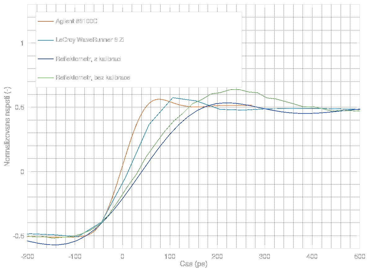
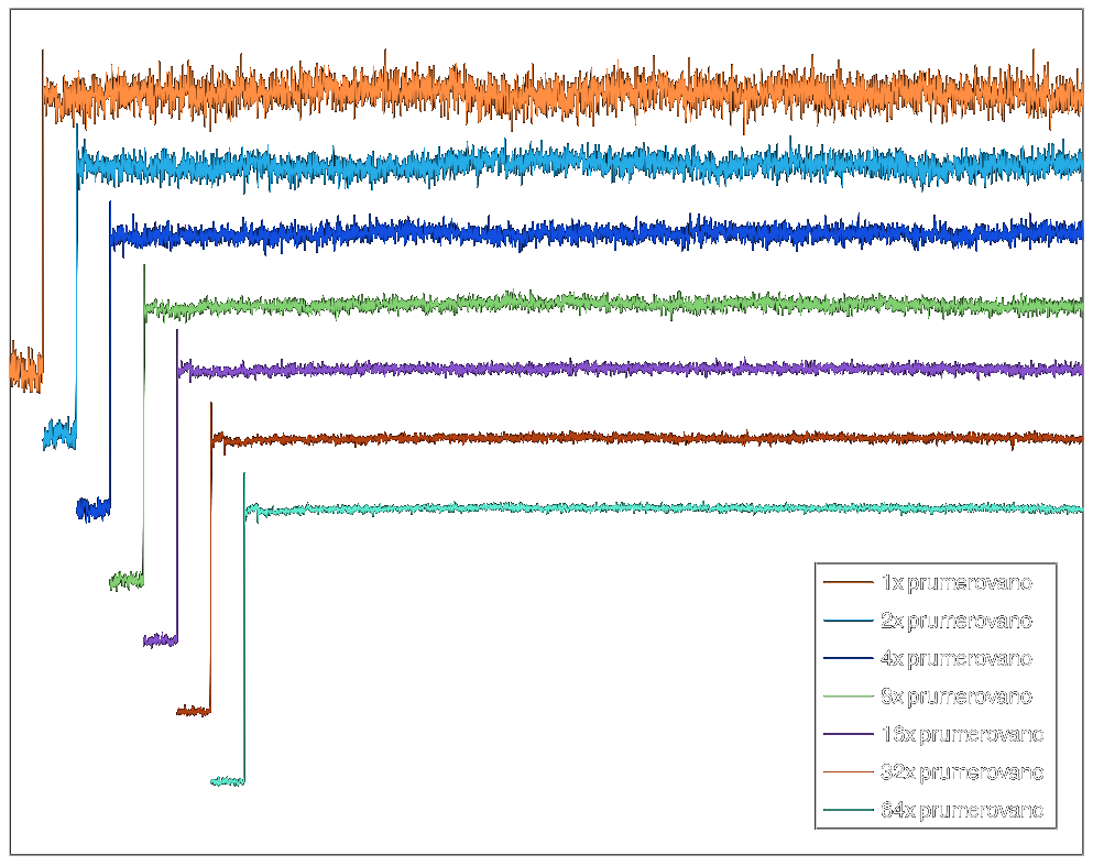
The orange and light blue ones were measured using commercial devices, the Agilent 86100C and LeCroy WaveRunner (this one was already mentioned last time). As you can see, the Agilent has the highest risetime (its bandwidth is about 26 GHz), about 89 ps which corresponds to the true waveform of the CML buffer pulse generator. Then the LeCroy, which cannot cope with the risetime and even shows low sample rate (about 25 GSa/s). The green trace is the reflectometer without SOL calibration and noise reduction, the risetimeis about 220 ps. The calibrated reflectometer output with noise reduction is slightly slower and shows pre-echo on the edge due to restricted spectrum.
Bandwidth and SNR
The SNR is a semi-measured parameter since it uses measured noise and estimated Gaussian pulse. The resulting SNR touches 0 dB at 2.5 GHz and goes under 0 dB near 3 GHz. So, the estimated useful frequency range is about 2-2.5 GHz.![]()
The resulting Wiener filter is nearly equal to 0 dB until 2-2.5 GHz and then sharply cuts off the spectrum. The resulting spectrum of the reflectometer after SOL calibration and noise reduction looks like this. The calibration seems valid until 2 GHz, then noise starts to emerge and the filter starts cutting it.![]()
Pulse generator parameters
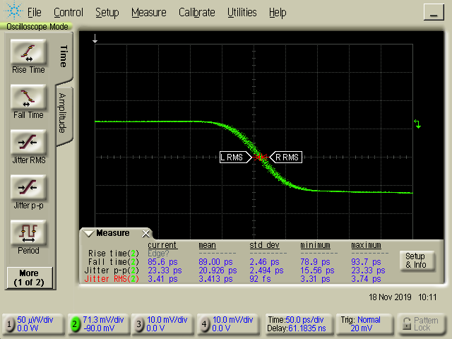
Here you can see the falling edge of the pulse generator, its fall time and its jitter. The jitter is measured between one unused output of the Si5351 and the pulse generator output. So, it doesn't tell us anything about jitter between the two VCOs of the 5351. I couldn't come up with any method of measurement of jitter between the two asynchronous outputs.
Test port impedance
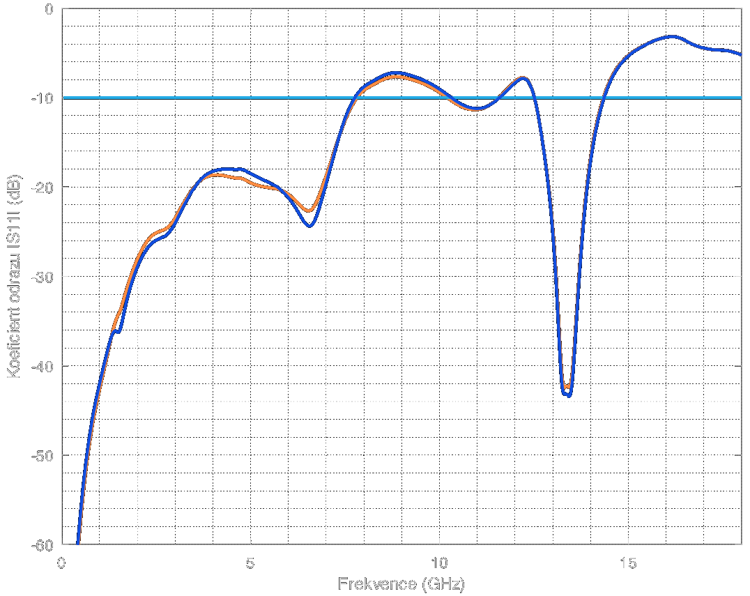
The input impedance looks quite good until 3.5 GHz. Since the working frequencies of the reflectometer are less than 3 GHz, the input match could be called as "better than -25 dB" which is extremely good. On gigher frequencies, you can see it gets really bad, mostly because of the bad footprint of the SMA connector. Also, the connector is the cheapest Chinese SMA connector ,which doesn't help much with the results. However, in the useable band, the match is quite good. Also, as you may have seen in the log about SOL calibration, the reflection is small enough to be completely suppressed by the calibration.
![]()
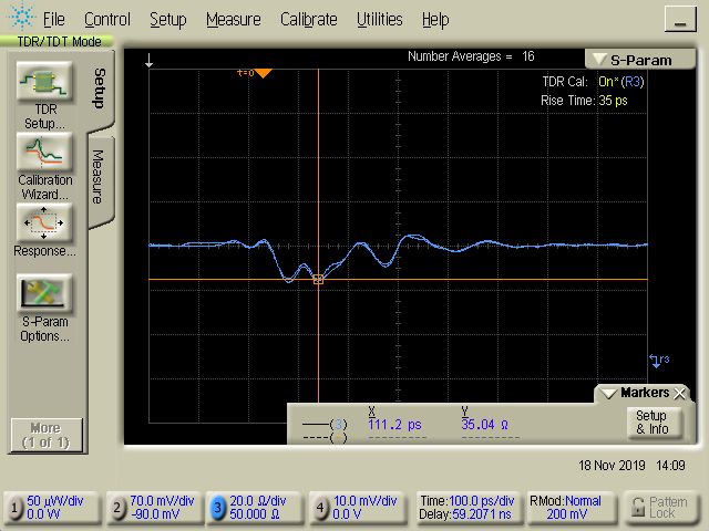
The TDR measurement of the port follows. The impedance drops to 35 Ohms for a while. The position of the impedance drop correlates with the SMA footprint on the PCB. The position was tested by using a sliding short and finding where the impedance drop lies. The sliding short was just the SMA torque wrench, no special piece of equipment. Another smaller impedance drop happens on the transition from the footprint to coplanar waveguide. One more impedance drop happens at the resistive splitter.
Noise reduction
The noise reduction comprises of averaging and Wiener filtering. The result of filtering is on the next graph. It helps, but is too time-consuming and doesn't get rid of all the noise.
![]()
The Wiener filtering suppresses the noise left after averaging. The filter looks at the averaging used for LOAD calibration, NOISE calibration and averaging used for the measurement itself. The filtering works for both calibrated and uncalibrated data.
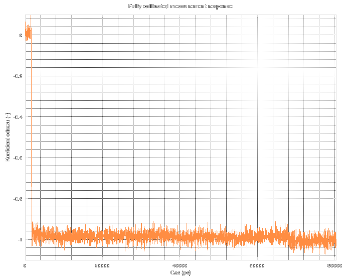
First, without noise reduction:
![]()
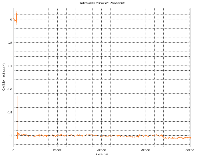
And with noise reduction:
![]()
The step at 68 ns happens because the original data ends there and the rest is a prediction of future events made by the Fourier transform. But I do not know why the step happens, I would expect the data to continue with the same level, just filled with noise.
Conclusion
The reflectometer works and it is usable from DC up to about 2 GHz (maybe slightly over that with reduced SNR). The time resolution is 20 ps and can store 4096 points. It can be calibrated as one-port VNA which removes the side effects of mismatched impedance of its input. An adaptive noise suppression algorithm was implemented.
What now?
Now, I will move onto next project. Maybe it will be two-port TDR/TDT usable as a time-domain VNA (hae to figure out the 12/16 element calibration process). Maybe it will be a two-channel oscilloscope. It will be most probably based upon designs of "loxodes", Darwin Sabanovic and Ted Yapo. All of these designs are practically the same, even with the same impractical bits here and there.
I already have a few ideas how to make the oscilloscope...
Now, I think I have already exhausted all the interesting themes of this project, so I will probably stop writing logs about this project and we could move on to discussion in comments section.
-
An appendix to the noise reduction which was cut too early
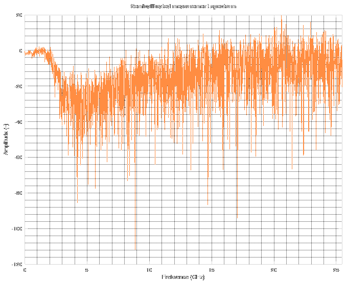
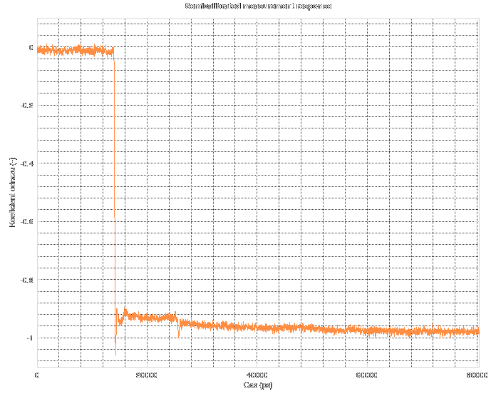
02/03/2020 at 15:33 • 0 commentsWhen I was talking about the Wiener deconvolution last time, I had it implemented, but not properly covered by analysis and graphs and therefore it did not contain as much information as I would like. A part of this appendix will repeat some statements from the last log, but in more detail and better-looking graphs. So, let's start with a graph of the measured spectrum. This one is a "semicalibrated" spectrum, which means that the "load" calibration has already been subtracted from the measurement, however the proper SOL calibration was not performed. The amplitude is logarithmic (and therefore in dB).
![]()
As you can see, it is not normalized to 0 anywhere in the spectrum. The spectrum looks kinda flat until 2 GHz, then falls off rapidly. Between 3 and 4 GHz, the signal completely sinks into something really nasty. It looks like random noise. Because it is. The reflectometer has useable frequency range up to about 2 GHz, then its response falls off and the rest of the spectrum is just random garbage not related to the measurement.
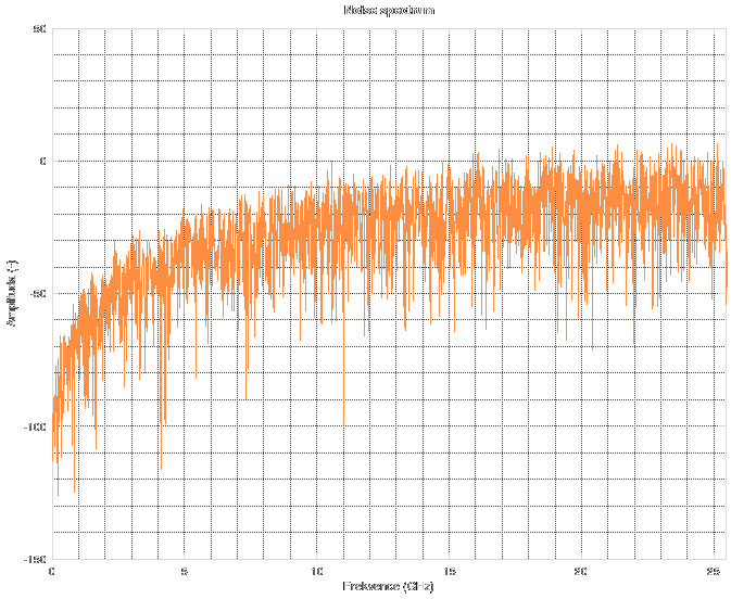
So you might ask how the noise spectrum really looks like. Here it is.
![]()
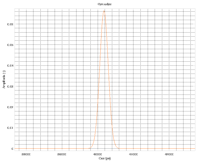
At low frequencies, it is quite subtle, but rises fast until about the 5 GHz mark, then stays almost constant. This is used for the estimation of SNR. The second part needed for SNR estimation is a Gaussian pulse or more specifically the probability density function which is a quit good model of derivation of the rectangular TDR impulse. Its best property is that once you integrate the pulse, you obtain a single real number, which is exactly 1. That means that you don't have to bother yourself with proper scaling of its spectrum amplitude-wise. Its spectrum starts at 0 dB and then falls off. The shape of the pulse is on next graph. Its width was figured out by experimentation asa compromise between amount of noise and effects of restrained spectrum on the data (pre-echo on edges, smoothed out features, longer risetime etc.).
![]()
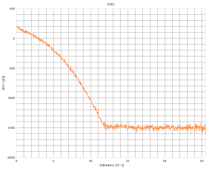
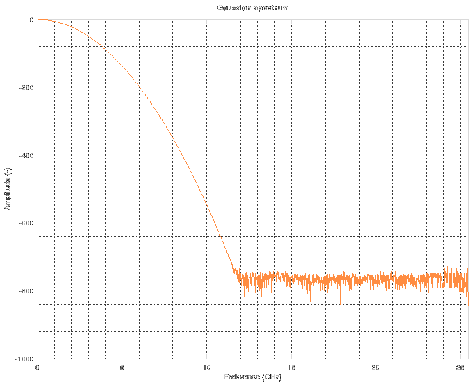
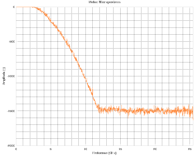
And its corresponding spectrum looks like this. Again, it is logarithmic and in dB.
![]() Forget about the spectrum above 11 GHz. The noise floor corresponds to "near-zero" values in floating-point computations during FFT. Simply said, it is the noise floor of floating point numbers. When you do something in floating point, stay aware of the fact that its precision is not infinite. There are cases when you might run into this issue and then you have to resort to arbitrary-precision mathematics which can be slow as hell.
Forget about the spectrum above 11 GHz. The noise floor corresponds to "near-zero" values in floating-point computations during FFT. Simply said, it is the noise floor of floating point numbers. When you do something in floating point, stay aware of the fact that its precision is not infinite. There are cases when you might run into this issue and then you have to resort to arbitrary-precision mathematics which can be slow as hell.
The gaussian spectrum and noise spectrum can be divided (element-wise, not matrix-wise) by each other to obtain SNR. You can see the estimated SNR in next graph, Y axis is logarithmic again. See how it reaches 0 at about 2.5-3 GHz. This is the point from which nonsense data prevail.![]() The resulting Wiener filter looks the like this.
The resulting Wiener filter looks the like this.![]()
As you can see, its response is unit (Y axis is logarithmic) and then it sharply falls off above 2 GHz. This means that anything above this frequency is cut off. The cutoff frequency and the shape of the filter depends on the estimation of the TDR pulse.
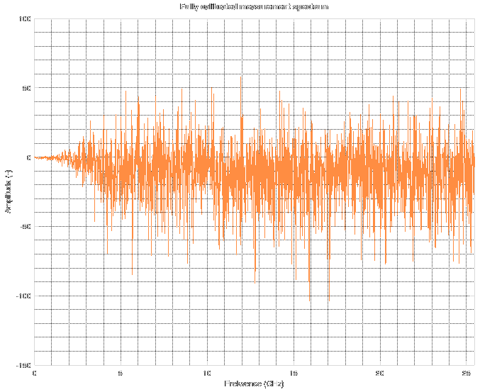
After the SOL calibration, the spectrum of the measurement looks like this. From about 1.5 Ghz you can see a fast onset of noise.
![]()
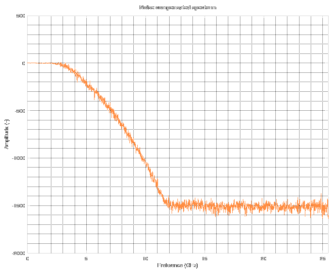
So, what happens if the Wiener filter is applied? The resulting spectrum is on the next graph.
![]()
As you can see, the calibration is "somewhat valid" up to 2 GHz and then it gets cut off by the Wiener filter. What does it do to the measured data? The measured data are on the next graph.
![]()
Nasty, isn't it? The large falling edge is response to short on the end of cable. As you can see, it does not reach -1. Then, you can see another, smaller reflection about 12 ns after the first one. That's a reflection caused by the reflectometer's test port having wrong impedance (about 35 Ohms for the footprint of the SMA connector). Then it somehow slowly creeps to the -1 mark. Sadly, I do not know the origin of this effect. Dielectric soaking? Maybe, but not expected on high-quality cable. Heating of the driving transistor inside the CML buffer? Could be.
Then, it gets corrected by the SOL calibration and the noise gets amplified. The reference plane position also gets corrected. It is non-zero after the calibration, because the short is connected after another piece of cable which delays the reflection. However, the peaking and resonance after the falling edge is gone. The secondary reflection caused by the reflectometer's non-ideal impedance is gone (which is THE ONE reason why I implemented the calibration). The slow "creeping" movement of the response is gone. Noise appears and also a new artifact on the end of the waveform - this is where the original data ends and the rest is only an approximation of future.
![]()
And when the filter gets applied...
![]()
As you can see, all of the out-of-band noise was removed and now the data starts to make some sense. You can even distinguish easily the point at 68 ns where the original data used to end. Now, the response is quite properly placed and scaled on both the 0 and -1 marks. The peaks on the falling edge are mostly due to effects of the restricted spectrum. The peak BEFORE the edge is completely made up by the calibration and noise reduction techniques, as it was not present in the original uncalibrated data. The peak AFTER the edge could partially be caused by the numeric operations, but it was substantially reduced compared to the original data.
You might be curious how the noise reduction affects the measured rising edge of the reflectometer. Let's have a look at a graph which will be also mentioned next time when I show some more measurements performed on the reflectometer.
![]()
The fastest rising edge belongs to the Agilent 86100C with TDR/sampling plug-in installed. It shows the real rising edge as emitted by the CML buffer. This is the reference for all the other traces.
The next slower one belongs to LeCroy Waverunner 6 Zi oscilloscope. The rising edge is quite fast, but slower than on the Agilent. However, even though LeCroy boasts its capability to sample "up to 40 GSa/s", it does not. Its samplerate is about 25 GSa/s and we were really trying to get the highest possible sample rate. Nope, not going to happen
The next, slower one is the reflectometer without calibration and noise reduction. You can see slower risetime, larger peak after the edge and some noise.
The last one is the reflectometer with calibration and noise reduction. Noise is gone, overshoot damped, everything is smoothed out. Risetime is slightly slower and preshoot appears. However, nothing dramatic.
Next time, I will probably have the master's degree exam done (planned for 6.2.2020), so I will probably finally write about the measured parameters (most of them were already at least once mentioned in logs) and about the result of the exam.
If you are sensitive, please do not read further. If you are thinking about buying any product of LeCroy, read further but be warned that several words from fecal vocabulary can be found throughout the text (I am not English-native so I could come up with maybe 30 words of this category in my language, but not in English, sorry).<RANT ALERT>
Honestly, the Lecroy is a piece of liquid sh*t which feels like it just came out of someone's a*se and still has a bit of. I wish I had a fast oscilloscope, but honestly, I would rather have a pile of t*rds sitting on my table than this piece of cr*p. It has one omnipotent semi-rotary-joystick-button-piece-of-rotten-sh*t as the main control.
And it is sooo ridiculous even though I owned 2 oscilloscopes, have everyday access to another 4 scopes in our makerspace, many others in my work and each made by different brand, so I should probably know how to use oscilloscope. Nah, that doesn't happen with LeCroy. It's even worse than the Agilent oscilloscope which lets you save a screenshot but delays the saving by several seconds which leaves you time to open some menus and then it saves the screenshots with the menus overlayed...
I can control right about any of the microwave measuring devices at the school department. Vector and scalar analyzers? Check. Noise analyzers? Check. TDRs and TDTs? Check. Various generators, detectors and any other possible equipment? Check. LeCroy t*rd? Not at all.
Trust me, I have used sh*tty chinese oscilloscopes with wonky rotary knobs which sometimes skip steps or do random magic due to noisy edges. These are bad, but still OK. Really, when something which costs nearly the same as the house you live in, you expect it could be more useable than chinese cr*p which costs about $500. Once you try to fiddle with any settings, you find out there is NO BUTTON TO GET BACK TO CHANNEL SETTINGS. Really. I tried pressing any and all of the buttons. I COULD get back to the channel settings, but either via some non-deterministic way of pressing buttons as if I was playing Mortal Kombat or Tekken. Sometimes, I could get back by disabling that channel and enabling it again. Sometimes not.
And the rest of the interface is as bad as this single piece of it. Look, if you want to know how a good minimalist interface looks, get your hands on the HP54100 from 1989 (!). Everything is deterministic and always has the same place. Everything, even the measurements, fits on the CRT and does not have to be placed in the graph area where you either cannot read it or it masks the trace. It was made in 1989, is driven by a Motorola 68000, has a CRT, less RAM than you ESP8266 and even then it is substantially than the Lecroy. Stay away from any blo*dy piece of en*ma which has a sticker "LeCroy" on it.
</RANT ALERT>
-
How Fourier transform can stab you in the back and one-port VNA calibration basics
01/26/2020 at 22:32 • 0 commentsLast time, I mentioned I was having some problems with the open-short-load calibration. I didn't know what was going on, supervisor of my diploma thesis had no clues as well and even none of my friends could help me. This time I will tell you the result of this log in the first article: I fixed it.
What was going wrong
When I performed the calibration, it seemed to be somewhat unstable. To make this statement less euphemistic, it was unusable, totally. After the calibration, I checked that applying the calibration onto the data used when performing the calibration, the result was correct. At t=0, there was the correct reflection coefficient and everywhere else were zeros.
However, after measuring the same calibration standard again (and even without disconnecting it and then reconnecting), the results were off. The peak reflection coefficient was slightly off from t=0, didn't reach 1 or -1 and was not a single-point peak. It was dispersed over several points.
Expectation can be the biggest mistake
I thought this was completely bad. However, it turned out that calibration cannot guarantee that the results will be perfect. It may look so in spectrum domain, but the end result in time domain can be quite unexpected. It was mostly my fault, because I was expecting too good results. And it looked really bad, because when the TDR response is shown as impulse response instead of step response, it looks different and not that intuitive.
So, I started with integrating the result after calibration. A simple algorithm which makes each point a sum of itself with the preceding point and iterating from t=0 to the end of the dataset did the job. However, the results were horrible. After re-measuring the calibration standards, everything looked quite normal.
![]()
But after connecting a cable between the calibration point (end of first cable) and the calibration standard, the result was covered in some periodic noise. And it was large!
![]()
Really, that makes no sense. Both I and my supervisor didn't know what was going on. I tried recreating the equations for calibration from 4 different articles/books only to come up with the same set equations in the end. I even checked them with wxMaxima (great tool, if you need something like Maple, go and get it), all looked OK. But the calibration didn't work. I thought there could be a problem with the FFT/IFFT but couldn't find out what it was. I thought it could be the DC part of the signal or the fact that the measured signal isn't periodic. So I thought I could use windowing in the FFT to mitigate this possible problem. However, when you look into the equations of the calibration, the windowing would disappear in the end (except for points where the window equals 0). So no luck using that. And so I thought it was just damned and that I'm an idiot.
Yesterday, I thought whether differentiating the measured dataset could help. Simply said, each point in the dataset after differentation equals its original value minus value of the previous point. And... it worked.
So, from this:
![]()
I got this:
![]()
It was not perfect, but substantially better. The "blip" on 16 ns caused by reflection on the connector of the reflectometer was gone. Overshoot and ringing on the edge? Gone. Noise? A lot of it emerged from nowhere.
So, the calibration started to work. However, there was a LOT of noise. Way too much noise.
When you feel like there is too much noise, get yourself a wiener
Sorry, it should be Wiener with large W. But I couldn't resist playing with the word. The proper term is Wiener deconvolution. In this case, it is a bit simplified. The deconvolution uses an estimation of spectrum of the original signal and spectrum of noise of the piece of equipment.
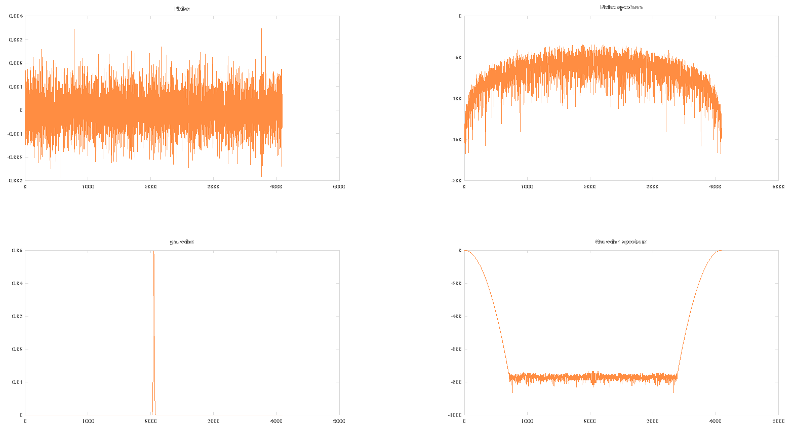
So, how it works? I expanded the calibration by one more standard called simply "Noise". First, you have to measure the "Load" standard on maximum averaging and saving it, then measuring the same standard without averaging and saving it as "noise". The software then subtracts these to get only noise. Then it is properly scaled according to the number of averages used when obtaining the "load" and "noise" standards. And the number of averages used when performing new measurement. To remind you, the noise lowers with 1/sqrt(N) where N is the number of averages. I thought it was 1/N and had a half-working code for several hours. The "load" standard is used as a reference of noise in the Wiener deconvolution and the "noise" ... as noise.
So, when the data is to be shown, you can check a new checkbox to enable the noise reduction. It doesn't matter if you run it on the calibrated or uncalibrated data, it works the same. And it works quite good.
![]()
Now the noise is heavily suppressed. Not completely, but it is acceptable now. Trying to get less noise also causes the waveform to be too smooth. The edges then get slower and slower, some small details are completely smoothed out and ringing reappers.
So, how does the damn Wiener work? The equation for the filter is
![]()
Multiply the spectrum of the measured data with this filter. The parts of spectrum where the signal reaches noise floor get heavily attenuated. So, noise is attenuated and clean signal is not. Remember, the SNR is a POWER variable so it depends quadratically on the noise and the reference signal.
This gets us back to the reference signal. What is it? Something that looks like the pulse from the pulse generator. I used probability density function. It is similar to the generated pulse and if you integrate it, the result equals to 1. So, it doesn't rescale the waveform.
![]()
In the graphs above, you can see the measured noise, its spectrum (it is the dual-sided FFT spectrum). Then the gaussian (not very well visible, sorry) and its spectrum.
![]()
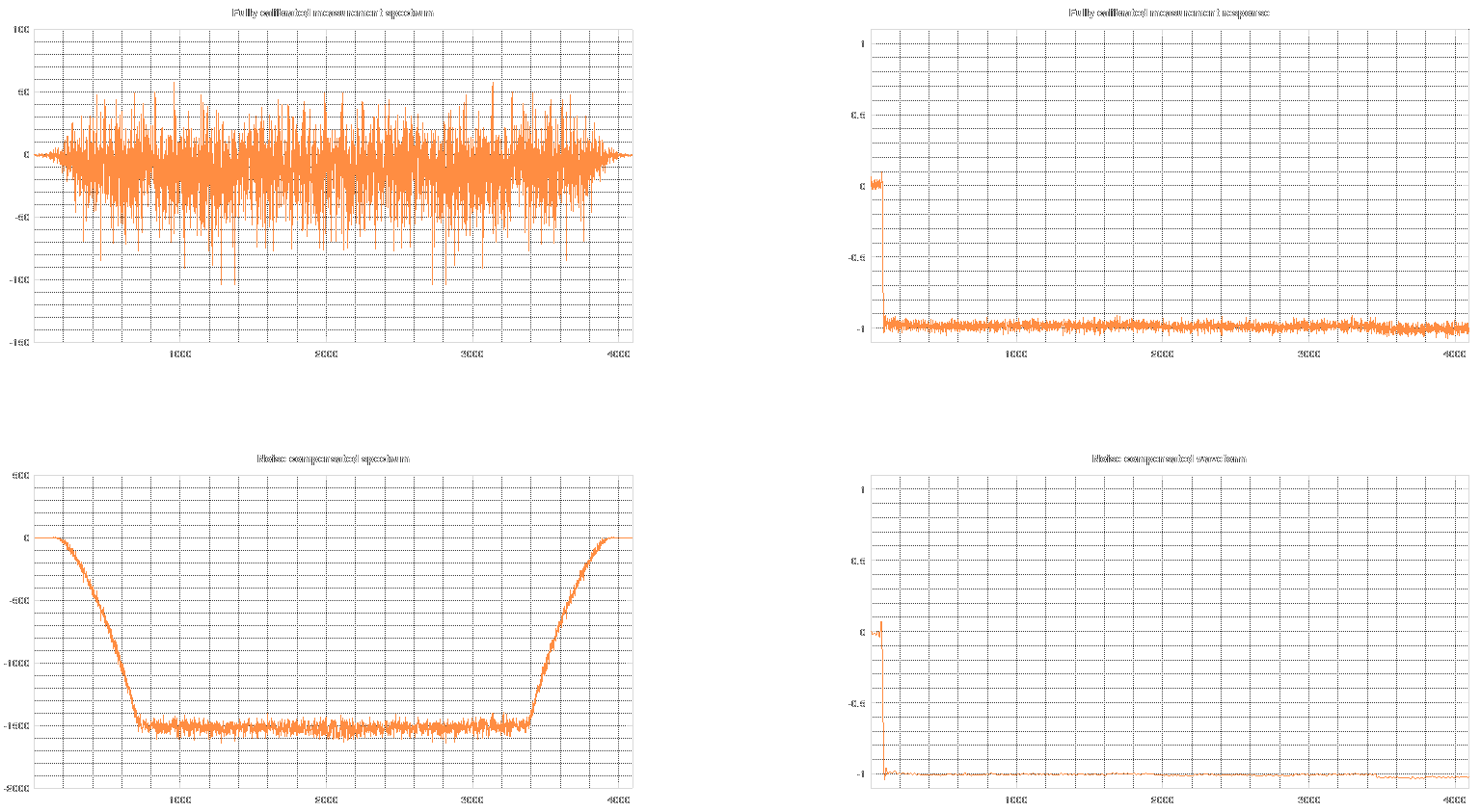
Now, in the graphs above, you can see the original spectrum and waveform of the calibrated waveform. under it, there is the version with reduced noise. As you can see, most of the spectrum is completely suppressed and the rest is bent so that it more closely represents the reference signal instead of noise.
To explain why the missing parts of spectrum aren't missed by me at all is simple. The reflectometer samples at 50 GSa/s. This allows noise up to 25 GHz. However, the bandwidth of the analog frontend is more like 2.5 GHz. This means that out of the 25 GHz bandwidth, 22.5 GHz of it is more or less only noise. And nobody likes noise (except in photos, noise reduction usually only hurts them).
One-port VNA calibration
The one-port calibration is simple for the user. Attach a calibration standard, measure it, save it. And do it for all three standards (and the noise!). Check a checkbox and it's done. However, inside the black box, a lot is going on. But only a small portion of it is the calibration itself.
S11L=fft([0 diff(calibration_data.load)]);
S11O=fft([0 diff(calibration_data.open)]);
S11S=fft([0 diff(calibration_data.short)]);
S11M=fft([0 diff(decoded_data)]);

Ed=S11L;
Er=2.*( ( (S11O-S11L).*(S11S - S11L) ) ./ (S11S-S11O) );
Es=-( (S11S+S11O-2.*S11L) ./ (S11S-S11O) );

S11A= (S11M-Ed) ./ ( Es.*(S11M-Ed)+Er );
As you can see, it takes the three standards, differentiates the and then gets their spectra. The same happens for the measured dataset. Then it calculates three error properties of a two-port error network. Three unknown vectors computed from three vectors. Then, it applies these three error properties onto the measured vector. And that's all.
Maybe you remember that a two-port network should be described by four parameters. However, since we are using only one port and can measure only in one way, we are only interested by going "through" the network only in one way. So, one of the variables is fixed to value 1 and made part of one of the three remaining parameters.
The result is that the DC offset, scaling error, reflections from the connector and cable and multiple reflections are suppressed. And the waveform also get sharpened. As much, as it can be sharpened. And that is why a lot of noise emerges. Sharpening amplifies high frequencies.
However, I will not give a complete lecture on VNA calibration since I am not an expert in this area.
See you soon in another log or project!
-
GUI should be for users, not against them
01/25/2020 at 20:01 • 0 commentsThe reflectometer has two GUIs. Each of them has a different usecase and therefore their usage slightly differs. One is a part of the firmware in the reflectometer, the other one is an Octave script which runs on a computer. Please remember that the reflectometer can run without computer or the Octave GUI.
The part of GUI in firmware
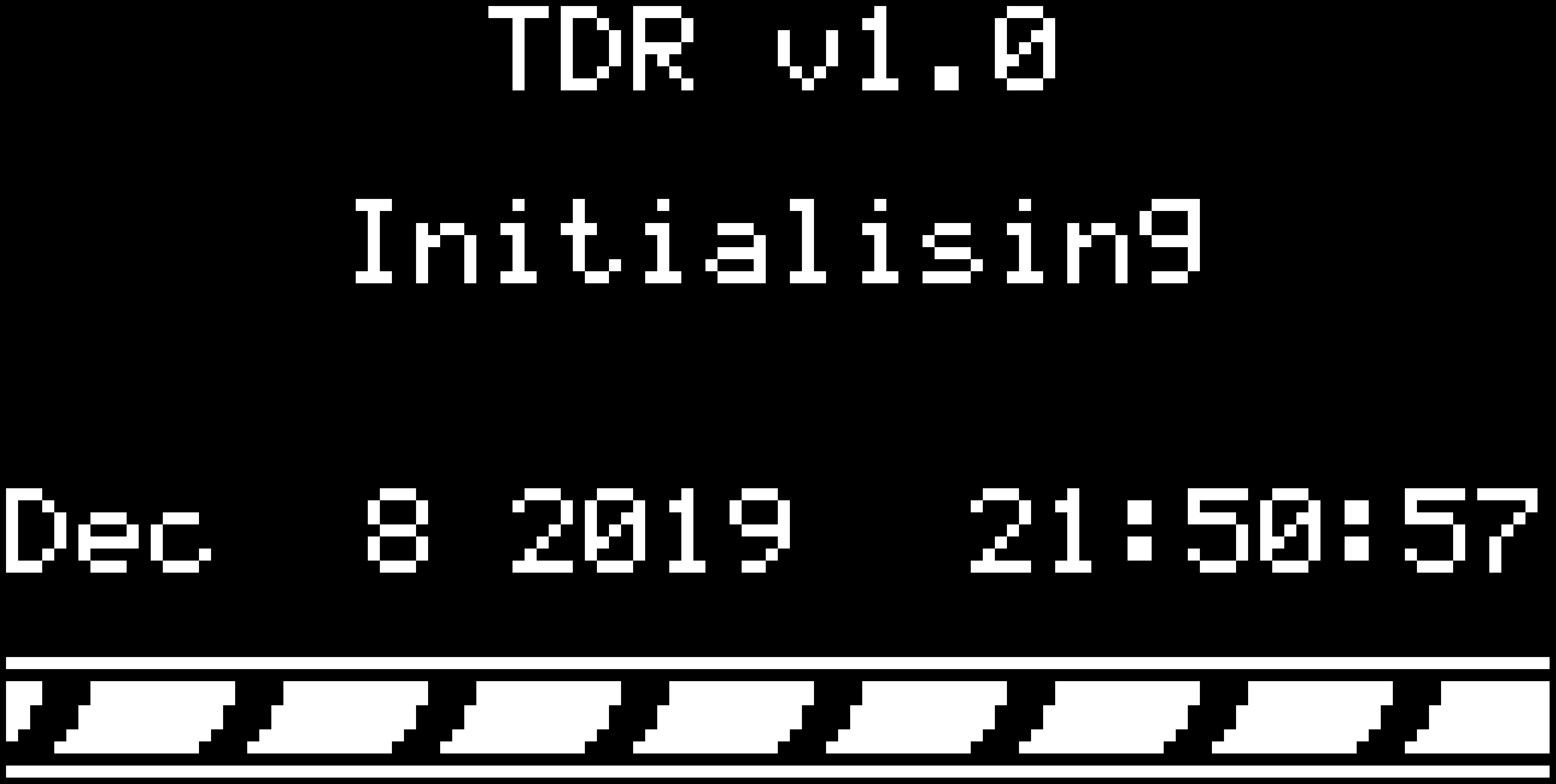
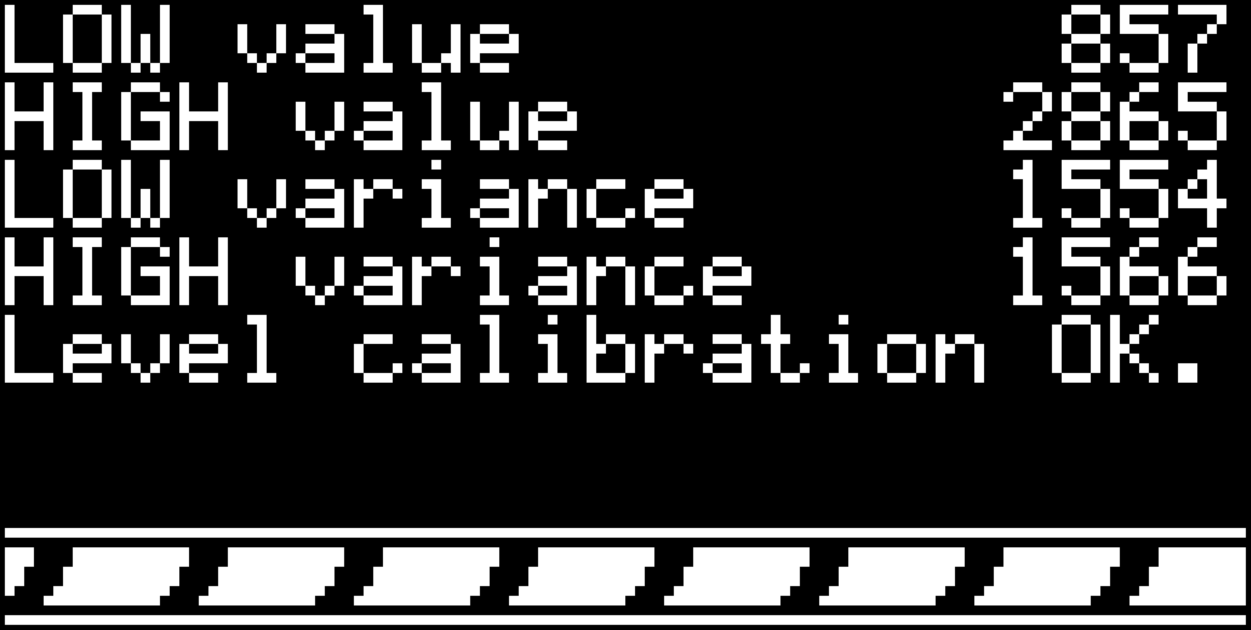
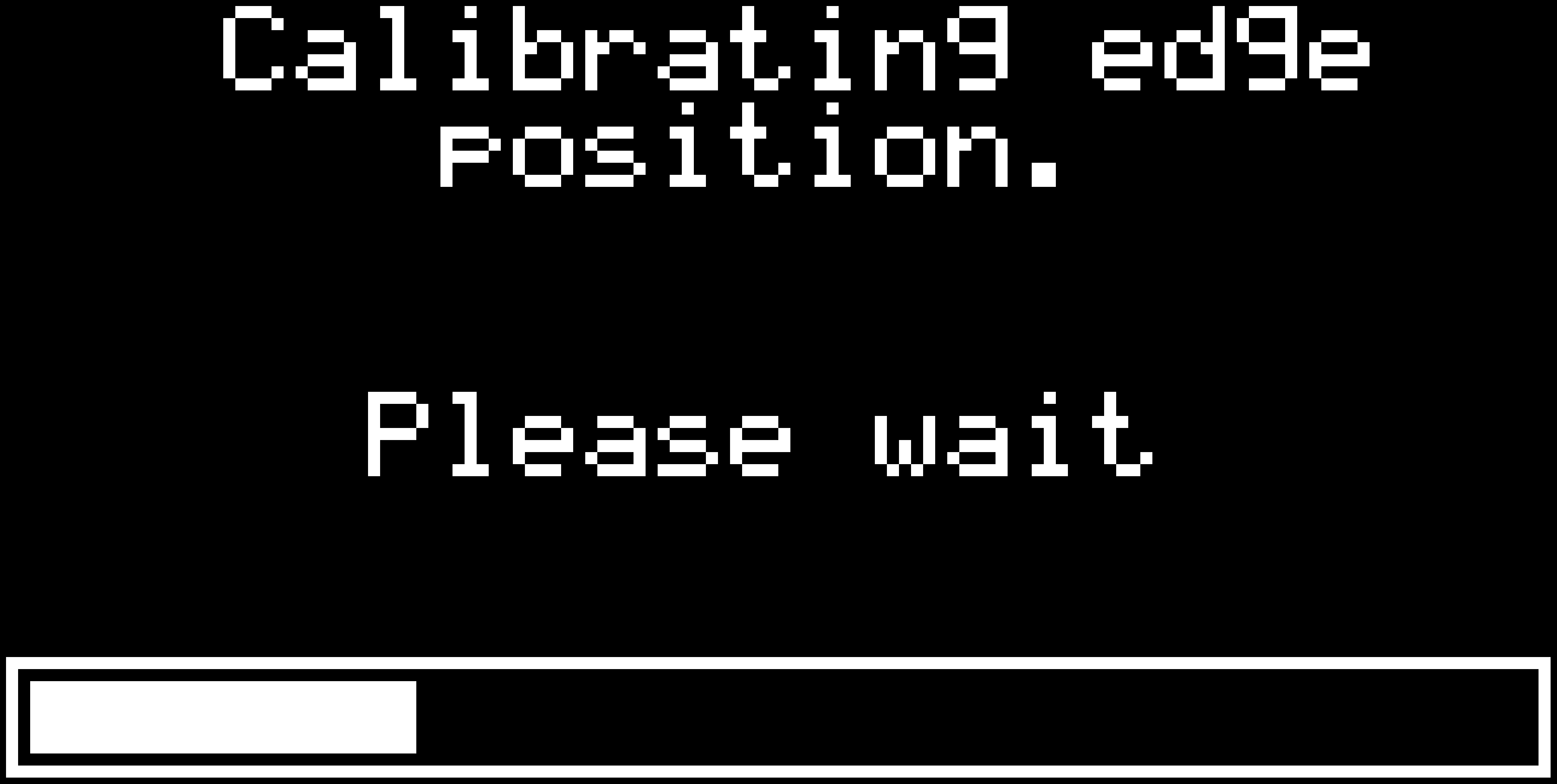
When the reflectometer is used without computer, it is meant to be used for detecting faults on cables hidden in walls and solving similar problems. Therefore, the GUI is minimalist. No menus, no options, no way to play with the reflectometer. It's meant to do its job and not more. It tells you about its current state, gives you commands during autocalibration and then allows you to run a measurement.
![]()
![]()
![]()
![]()
![]()
![]()
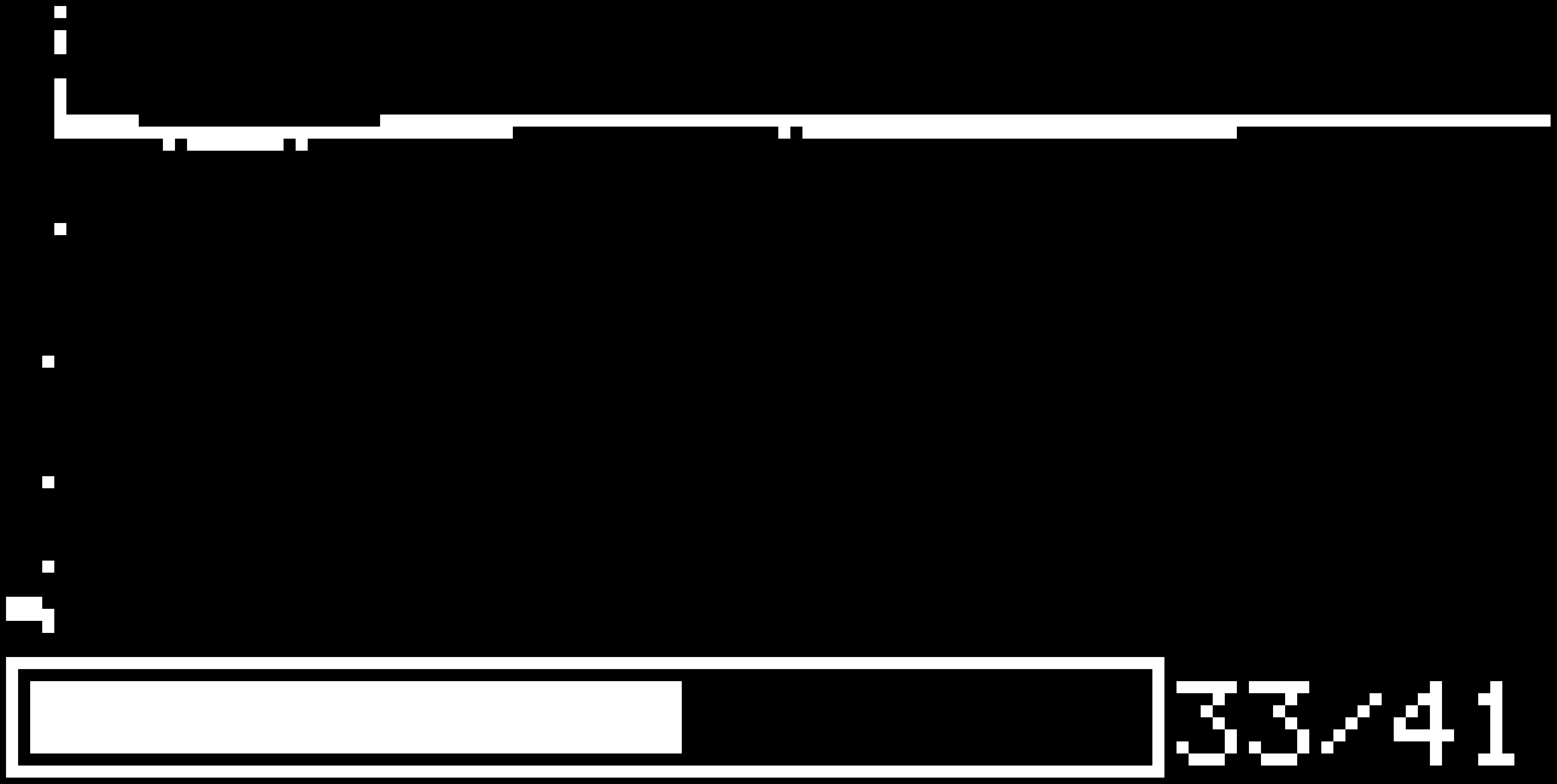
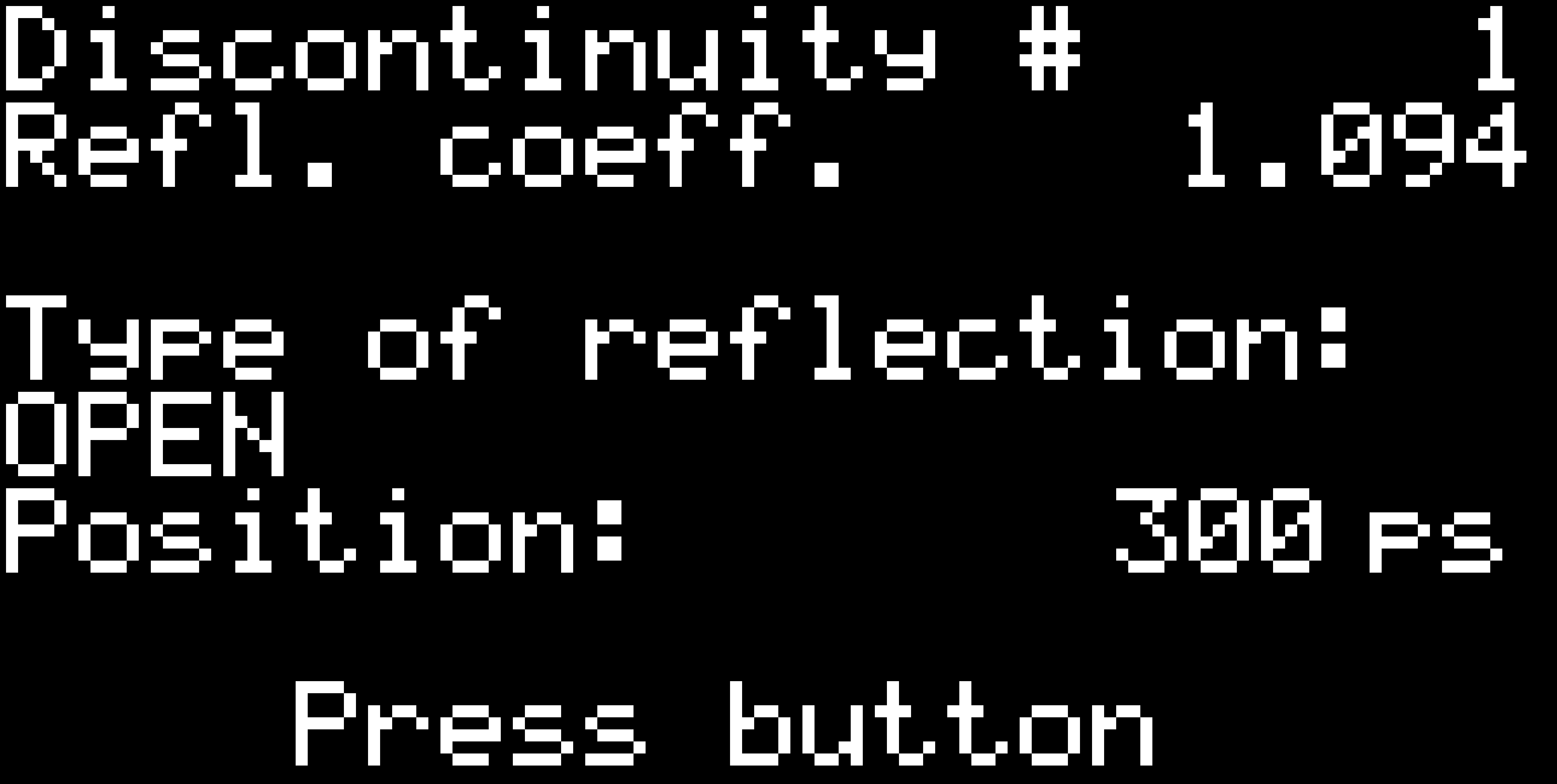
When the measurement is done, you will be presented with the measured data. The GUI zooms in the data so that each pixel equals one sample (the smooth zooming effect is quite nice) and then scrolls from the beginning of the measured data up to the first found discontinuity, waits there for a while, then shows you the measured reflection coefficient and the position of the discontinuity in the cable. The position is given in picoseconds, because the reflectometer knows nothing about the cable including the phase velocity in the cable. So it's up to you to calculate the spatial position of the discontinuity.
![]()
![]() As you can see, it tries to detect the type of the discontinuity. It can detect "open", "short", "doubled impedance", "halved impedance" and for other cases it only shows "higher impedance" or "lower impedance".
As you can see, it tries to detect the type of the discontinuity. It can detect "open", "short", "doubled impedance", "halved impedance" and for other cases it only shows "higher impedance" or "lower impedance".The position given in time and not in spatial dimensions is not a serious limitation of the firmware, since there are only two ways to measure the physical length of a cable using one-port measurement. The simple one is a case when you know the type of the cable and its velocity factor. The other one requires measuring the total physical length of the cable and then trying to measure the total electrical length, which might be impossible in case of heavily damaged cable. Adding this feature would require an input method for typing numbers (the built reflectometer has only one button). Using a calculator or multiplying in one's head sounds more reasonable to me than adding a keyboard, but I expect someone could argue that I should have added the keyboard (and yes, I could have).
And that's all it does. Simple, easy to use, self-explaining, guides the user from power-on to results. For more involved analysis, there is the second GUI.
Octave GUI
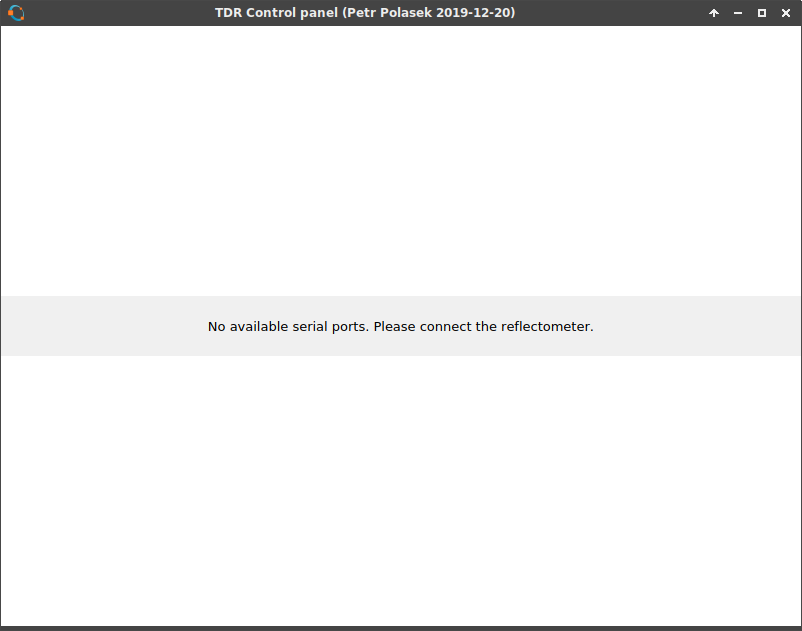
This GUI runs as an Octave script on computer. Theoretically, it can run on anything that has USB, runs Linux and has Octave with support for serial ports. Once you launch it, you are greeted with a window telling you to connect the reflectometer. Well, not greeted, but... well, at least it tells you so. It's not an example of good looking GUI, but I don't count myself as a programmer and even less an artist so please excuse that.
![]() And it can even tell you if you are running the Octave binary from Flatpak with restricted access to serial ports and tells you how to correct it.
And it can even tell you if you are running the Octave binary from Flatpak with restricted access to serial ports and tells you how to correct it.![]()
If there are other available virtual serial ports, it probes them if they are connected to the reflectometer. If not, it waits for you to connect the reflectometer. After a new serial port appears, it tries to connect to it. If it is the reflectometer, it tries to connect to it.
![]() After a handshake is performed, the GUI tells you the version of the firmware (time of compilation) and then finally connects to the reflectometer.
After a handshake is performed, the GUI tells you the version of the firmware (time of compilation) and then finally connects to the reflectometer.![]()
You may ask what happens to the reflectometer after the computer has connected. Is it paralyzed and can be controlled only from computer? The answer is no. It only knows that it is remotely controlled and can still be controlled using the physical button (the Octave script expects it as well and won't start to behave funny). The whole state machine of the autocalibration procedure and measurement is running inside the reflectometer, so nothing will happen even if the Octave script fails and stops. Just start it again and the Octave script will ask the reflectometer about its state and then continues where it left off.
There is only one difference between the reflectometer's behaviour when running with computer. It doesn't run the graphical representation of measured data after the measurement has completed. Instead it waits for the computer to download the measured data (and the firmware tells you about it graphically, again). So technically, it is possible to get into state when you have shut down the script and the reflectometer waits infinitely for the computer. I will probably change this behaviour later.
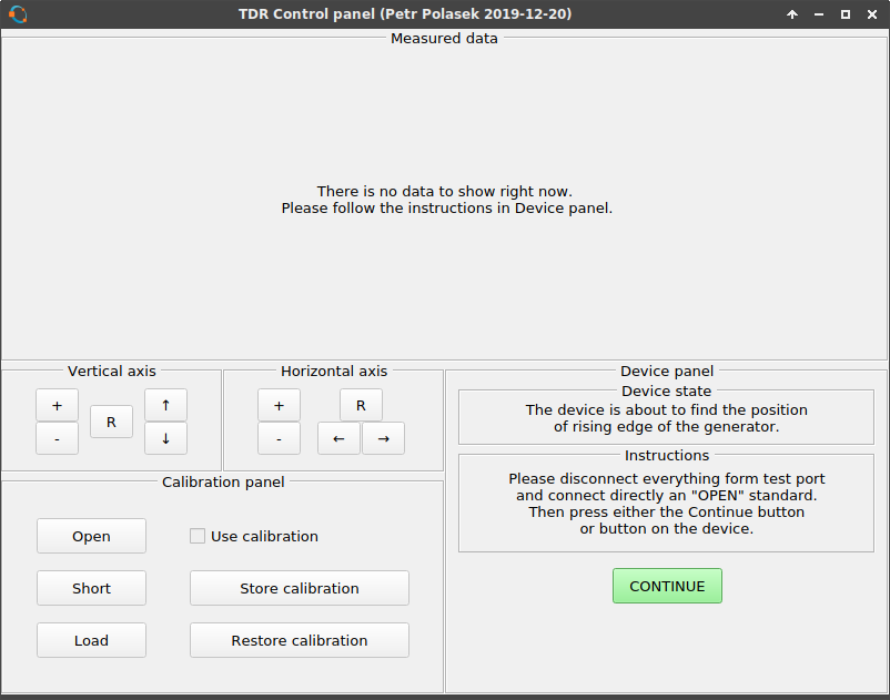
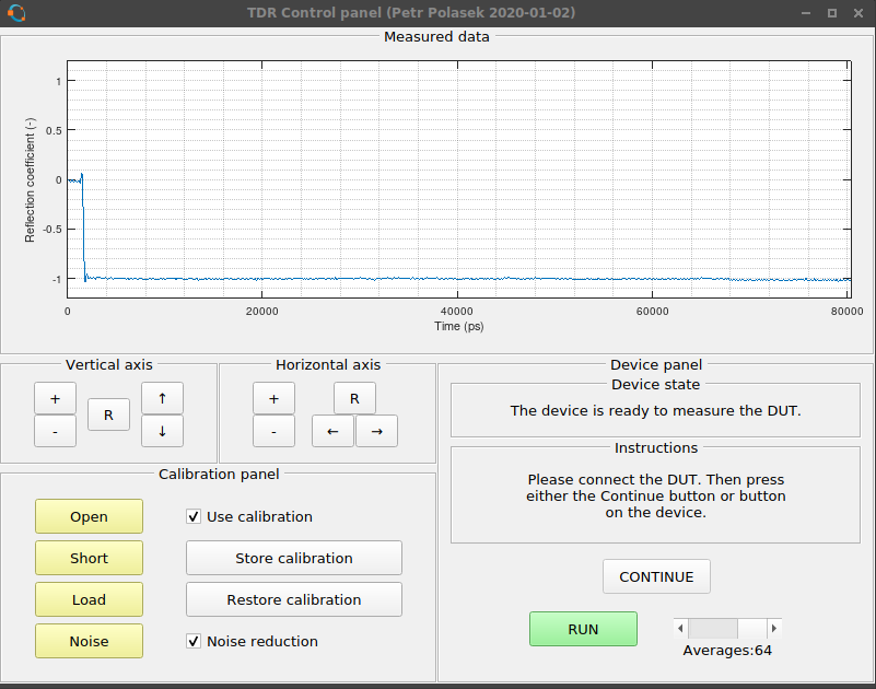
The Octave GUI also tells you about all the steps of autocalibration and gives you orders what to do. And all of the buttons which should not be clickable at any moment are properly disabled and are not clickable.
![]()
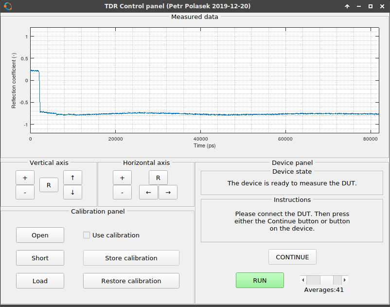
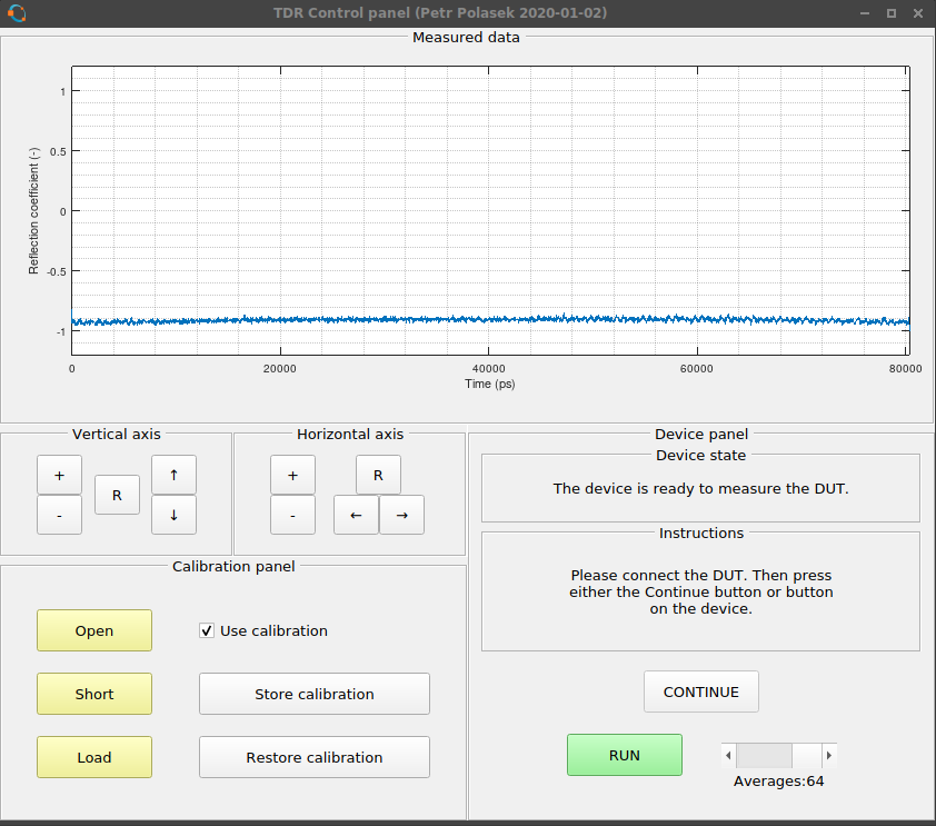
When you get to the point where you can run a measurement, you can even set the number of averages (it defaults to the optimal number calculated during autocalibration). It can be set in range 1-64. Maybe I will patch both the firmware and the GUI to allow more than 64 averages.
![]()
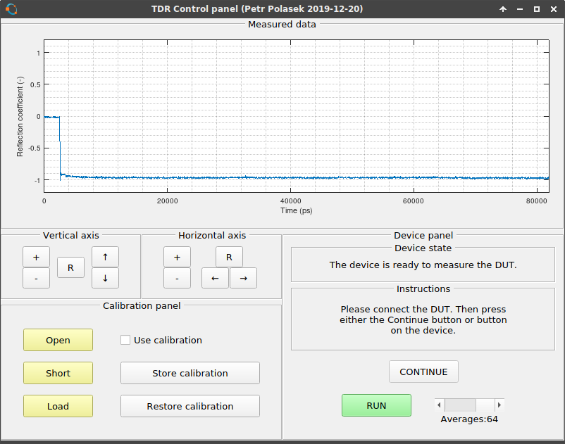
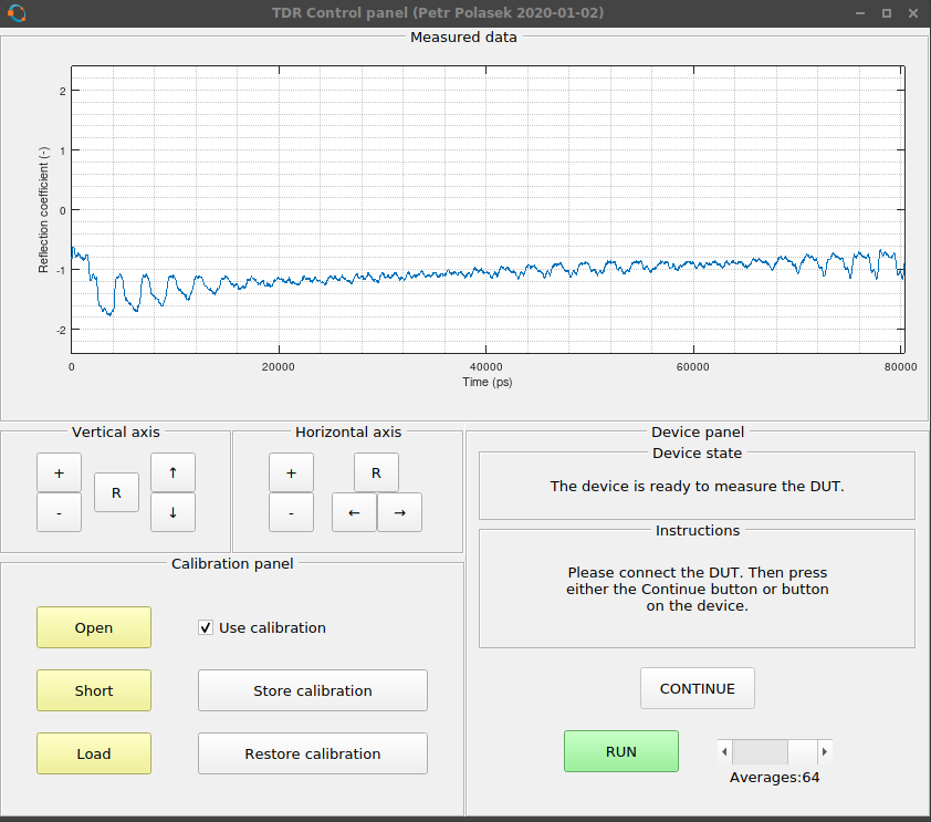
On the picture, you can see the measured data. It is slightly DC offset from the correc tposition and has a nasty distorted waveform. That can be easily fixed by performing "Load" calibration. That works by measuring the 50 Ohm standard and pressing the "Load" button. This stores the measured data and automatically applies this standard to the measured data by subtracting the standard from the measurement. Whenever a calibration is stored, its button turns yellow to signal that it has already been done. You can see the effect of applying the "Load" standard to the measurement. The waveform is no more "wavy", it is almost flat now. And the DC offset is gone as well. However, this is only a simple calibration which has very limited abilities.
![]()
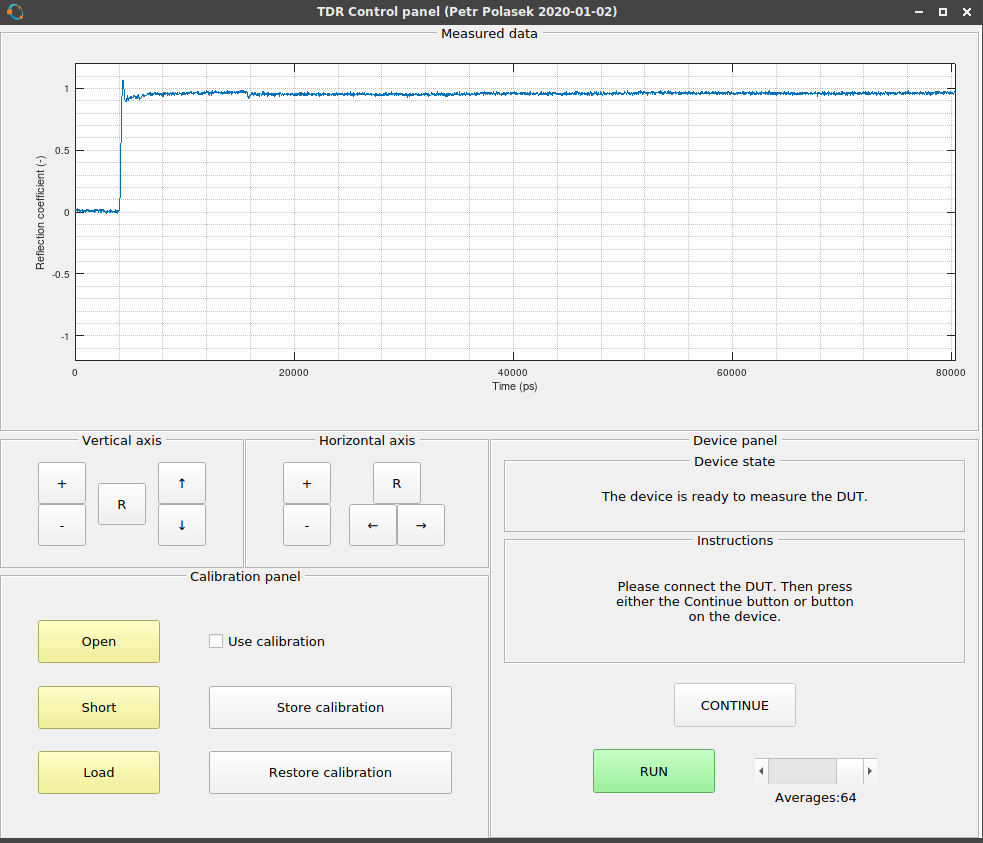
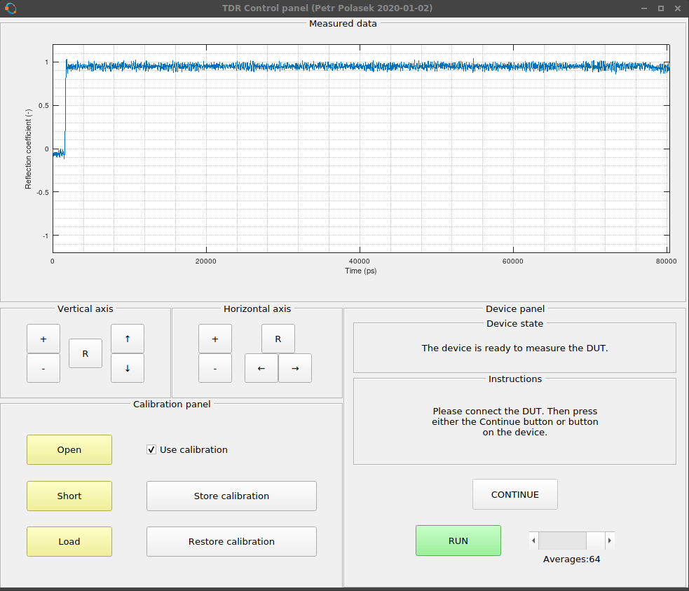
The GUI also has a standard open-short-load calibration algorithm built in, however it seems a bit broken to me. First problem is that the version you can find both on Github during the time of writing and here as a ZIP file shows the data after calibration in form of impulse response instead of step response. Therefore the data look different from what you would expect from TDR. This can be fixed easily by showing the data as a cumulative sum (each point is a sum of the preceding point with itself). This corrects it back to step response. However, the measurement is "bent", probably due to some mistake when playing with all the FFTs and IFFTs. I think that the FFT doesn't like the step waveform with non-zero average and the calibration then causes some non-existent low frequency components to emerge. I am going to fix this as well.
Of course, the calibration can only be applied once all three calibration standards have been measured. The standards can be removed by clicking on its corresponding button again. The calibration can be stored to file or retrieved from it, however no way for defining your own file has been implemented. The reason is that at each boot, the DC offset and the time offset of the rising edge can be slightly different, thus invalidating the calibration. Therefore, storing or retrieving the calibration is only usable during the time the reflectometer is running. So, no ability to use more calibration files was implemented.
The graph can be interacted with by using the buttons on the "Vertical axis" and "Horizontal axis" panels. It allows you to zoom in and out (each time zooming in or out by a factor of 2) and also shift the axis (shifting happens by shifting by one half of the range being shown). There is also a useful "R" button for resetting the axis once you get tired of playing with the graph. It gets reset also by performing a new measurement. I should probably fix that as well.
Next time, we will probably meet with measured parameters.
-
What happens in software, stays in software
01/22/2020 at 15:49 • 0 commentsIntro
As you might have already noticed, the hardware is quite simple. Usually this either means you are looking at a non-complete prototype which will need additional bugfixes or that there is a lot of work done by software. This project aims to be of the second kind, however I won't pretend it shows some signs of the first kind.
Synchronous sampling on STM32F103
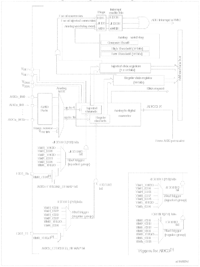
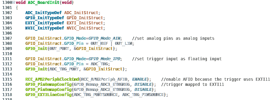
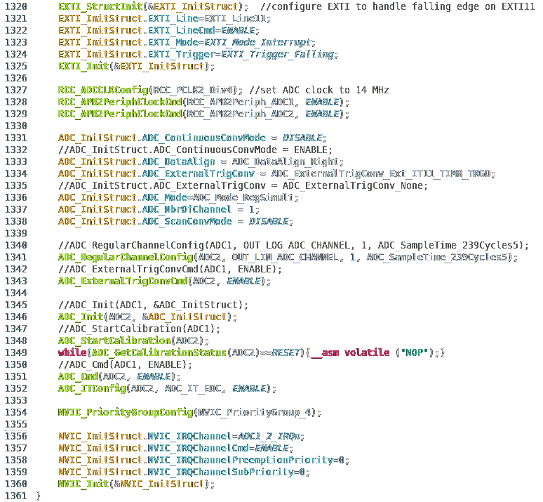
"An image is worth a thousand head-sratches." It's quite obvious how to use external ADC triggering on STM32F1 from the image. Or maybe not at all. Let's start by stating that you have to enable the ADC, connect it to appropriate input pins, connecting the trigger to EXTI11 and configuring the NVIC to handle ADC interrupts. More after the image. You might want to make yourself a large mug of coffee.
![]()
First you have to enable the clock to the port with analog pins and AFIO (alternate function configuration peripheral). Then set the analog pins as "analog inputs" and the trigger pin as "floating input" or better connect a pull-up or pull-down. For those familiar with STM32 - if you were expecting the trigger pin to be set as "alternate function", you were wrong. It doesn't work that way. In any case, don't expect to find this piece of information in datasheet or reference manual. Then you have to remap the trigger of ADCs to the external trigger on EXTI11 input. Maybe it will seem simpler once you see the source code (there is no code to enable clock to the ports used, because they are already on).
![]()
At this moment, it is all connected together, but can't trigger yet nor measure anything. What's missing? The trigger has to be enabled and the trigger condition has to be selected. ADC must be enabled, configured and calibrated. Interrupts need to be configured and enabled.
So just set up the EXTI to react to falling edge on EXTI11 and initialize it. Enable ADC clock and set the ADC to trigger using the external trigger. Then set the sample time length and initialize the ADC. Then it has to be calibrated (internal procedure of the microcontroller). Then one has to wait for the calibration to wait. An anti-optimization measure is included. Then enable the ADC interrupt, configure NVIC to watch the ADC EOC interrupt flag and enable it.
![]()
Now the microcontroller is ready to measure voltage using the ADC after being triggered using the external trigger, then run an interrupt which does some magic with the result. It could also perform a transfer using the DMA, but there are reasons why I used just an interrupt.
Logic in the interrupt
I won't explain the whole logic in the interrupt, because the state machine is a bit complicated. Let's concentrate on the practical part of the job.
The measured data are 10 microseconds long and contain 500000 values 20 ps apart. Since the Si5351 PLL VCOs start with unknown phase offset, it is not known where the beginning of the measurement lies in the dataset. There is also one thing worth mentioning. One sample occupies two bytes and the whole dataset occupies 1 MB of RAM. The F103 has only 20 kB of RAM and you cannot allocate all of it for the sampled data. Therefore you cannot sample the whole dataset and then try to find something in it. It has to be done vice versa.
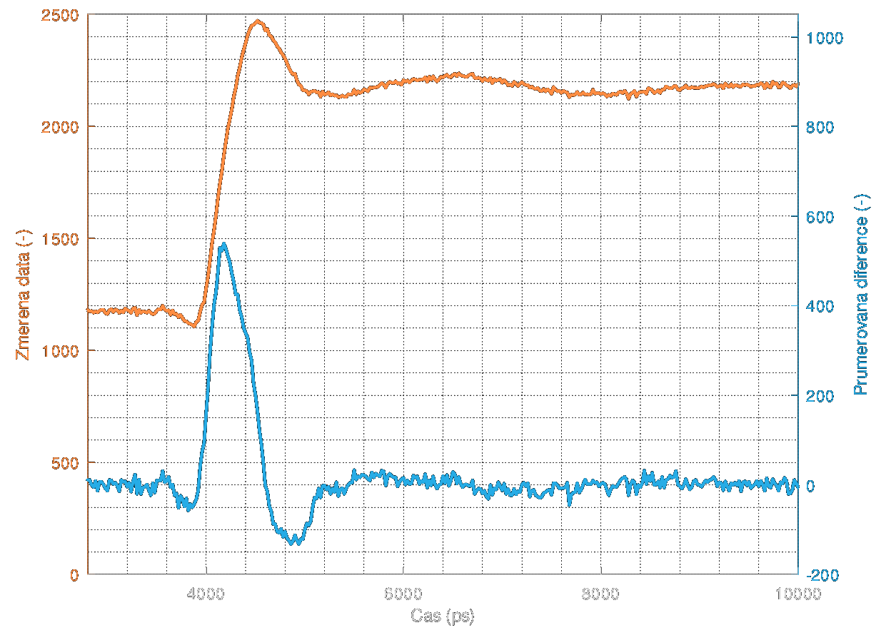
The interrupt tries to find a point where the data contains the largest derivation. Because of large amount of noise, it uses average of 16 first-order differences. After a bit of thought, an equivalent of this average is a difference of two values 16 points apart. The equation below should prove that.
![]()
Measurement plane position calibration
Now we will leave the interrupt for a while. During autocalibration phase, the firmware tries to roughly find the beginning of the dataset by collecting the position of the largest differentiation over several runs. Again, this is because of noise in the dataset. Then it asks the user to connect a cable. Then it performs several runs of measurement. In the measured data, the firmware tries to find the rising edge corresponding to the end of the cable. Using the voltage before and after the rising edge and its risetime, it selects a point before the rising edge as starting point of the measurement.
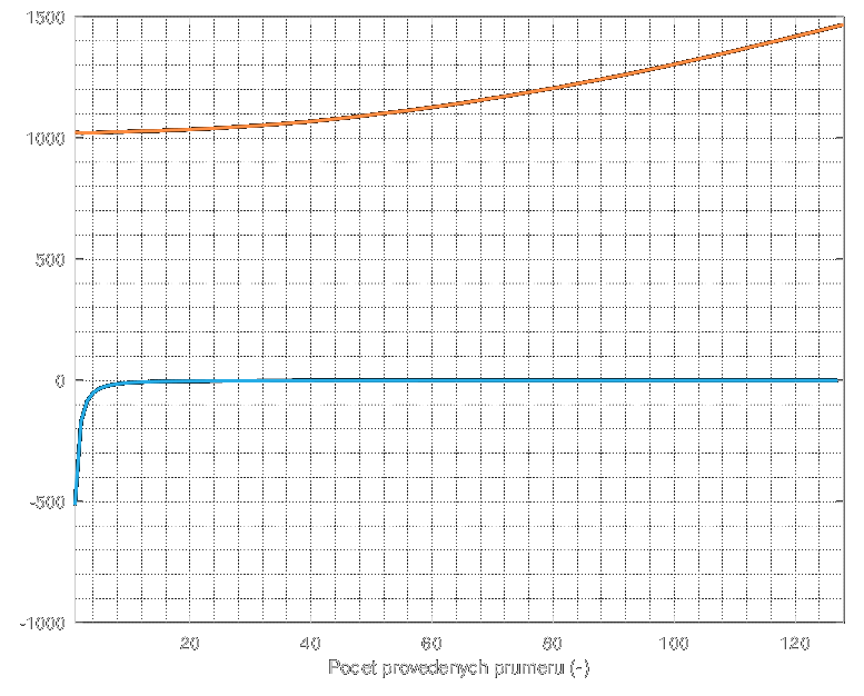
Back to the interrupt. To see what the interrupt sees from the differentiation, look at the next graph. The peak in the middle of the rising edge is quite easy to detect. The measured data are orange while the difference is blue. Again, sorry for Czech captions.
![]()
DC offset autocalibration
Before this part of autocalibration, there is one thing to do. The buffer amplifier with BF998 has its current source driven by DAC. The firmware first increases the current until the voltage during HIGH logic value gets safely under the higher limit of the ADC range. Then it measures the voltage during the LOW logic value. The current is increased/decreased until both voltages are symmetrically far from the half of the range of the ADC.
Noise level estimation
During the DC autocalibration, 4096 measurements are performed for each logical value. This gets a quite precise average voltage. Then, another 4096 measurements are performed which are used to calculate variation of the measured data. This serves as noise level estimation.
Averaging
The firmware uses averaging method which was used in 1980s in oscilloscopes made by HP. It stores only the averaged dataset and not all of the runs performed. If you are thinking it's "moving average", it's not. That would require storing all the measured runs. Exponential moving average would be closer. However the algorithm changes the weight of the stored data and new measurement so that in the end, the result is an arithmetic average of all the runs. And some noise caused by rounding errors.
The algorithm can be seen in the next equation. i is the current number of runs, x is the current sample and y is the stored data.
![]()
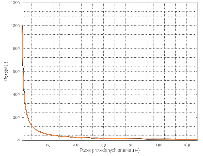
You might be curious what the averaging does to variation. The variation decreases as a function 1/N where N is the number of averages performed.
![]()
This function looks the same both when run in floating point and when run in integer mode. Not so when you look closely. If you multiply the variation by number of averages, you should get a constant function. Well, that happens when you run the averaging in floating point. When run with integers, you can expect some dark magic to start happening. And it does. The blue line is a differentiation of the variation while the orange line is the variation multiplied by the number of averages.
![]()
Oh boy, that's bad. You probably expect a lot of noise to emerge when running more than 50 averages or so. And yet you are completely wrong. The increasing curve only means that the noise gets dominated by the rounding errors instead of the measurement noise. Therefore, the noise present in the dataset is getting lower and lower until it hits a lower limit imposed by the rounding error. The noise could be theoretically as low as a few LSB. So, no big trouble. However, there is an optimal amount of averaging. You can see that the noise doesn't get much lower after more than 10 averages. And the rounding errors start to rise after more than 20 averages. These numbers change with the variation on the beginning. Or more precisely, on its square root - that's the standard deviation you are familiar with.
The optimal seems to be between around one half of the standard deviation.
Level autocalibration
During the DC autocalibration, the values for LOW and HIGH logic levels on the pulse generator are measured. These voltages should be equal to voltage measured after OPEN and SHORT calibration standards. And it works... quite enough. You can see the response to open end of cable.
![]()
It's not perfect, but good enough for automatic finding of discontinuities.
Discontinuity detection
The software measures the dataset, then tries to find the largest differentiation point. Then it tries to find the next largest differentiation point excluding some tolerance field around the first discontinuity. This happens 8 times. The differentiations get sorted by the time they appear on (yes, I used bubblesort, no need to implement anything faster here). It's not very precise due to the limited calibration, but good enough to detect simple discontinuities. On a properly calibrated reflectometer, reflection coefficient outside the range <-1;1> should scare you. But since this is not properly calibrated, it's kinda OK.
![]()
See you next time. The next post should concentrate on the user interface on both the device itself and the Octave application.
-
What should one do with the sampled voltage and caveats of samplers
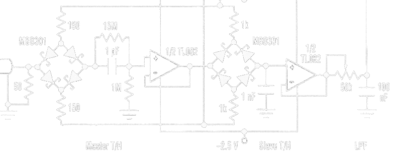
01/12/2020 at 23:46 • 0 commentsLast time, we've got covered the method for sampling using diodes. However, that's only the beginning of sampling. Then you need to sample into something and then use it for something. Of course, it has to be a capacitor or something capacitor-like. This means you can sample into capacitor, gate of field-effect transistor, input of unipolar op-amp etc. I already mentioned the Houten's sampling head, which uses input of TL072 as sampling capacitor. However, its capacity is about 15 pF. This would heavily load the sampling bridge and also the input of the sampling head. Therefore the sampling head uses another 1 pF capacitor in series with the op-amp, which forms a capacitive divider and also limits loading the sampling bridge.
![]()
There is a reason why use a unipolar amplifier. You have to store the sampled voltage, but that's only one part of the job. After storing the voltage, you want to read it, probably. Well, unless you are Schrödinger's relative and don't actually want to know the voltage. Speaking of Schrödinger, that is the problem. Reading the voltage will probably somehow alter the sampled voltage. If you use bipolar amplifier after the sampling circuit, you will experience an effect called droop. Because a bipolar amplifier has a significant input current (remember, the sampling capacitor is only a few picoFarads), the sampling capacitor gets gradually charged (or discharged). If the time between sampling the voltage and measurement is always the same, you will obtain the data DC shifted, downscaled or mix of both. If the time between those events is not constant, the data will look as if they were noisy. The noise is approximately equal to the droop rate multiplied by the jitter of the time between sampling and measurement (if the droop is approximately linear).
Therefore there are two things you want to avoid. Input current of amplifier after the sampling circuit should ideally be zero and the time between sampling and measurement of the sampled voltage should be constant. And as short as possible.
This leads us back to the unipolar amplifiers. These have almost no input current, or at least negligible if the time between sampling and measurement is short enough. You can use MOSFETs, most JFETs, MOSFETs and most unipolar op-amps. However, avoid HEMTs, even if they are called field effect, since their input current is almost the same as in bipolar transistors. Or at least this applies to those which have a proper datasheet (many have only a few limiting values and a set of S-parameters).
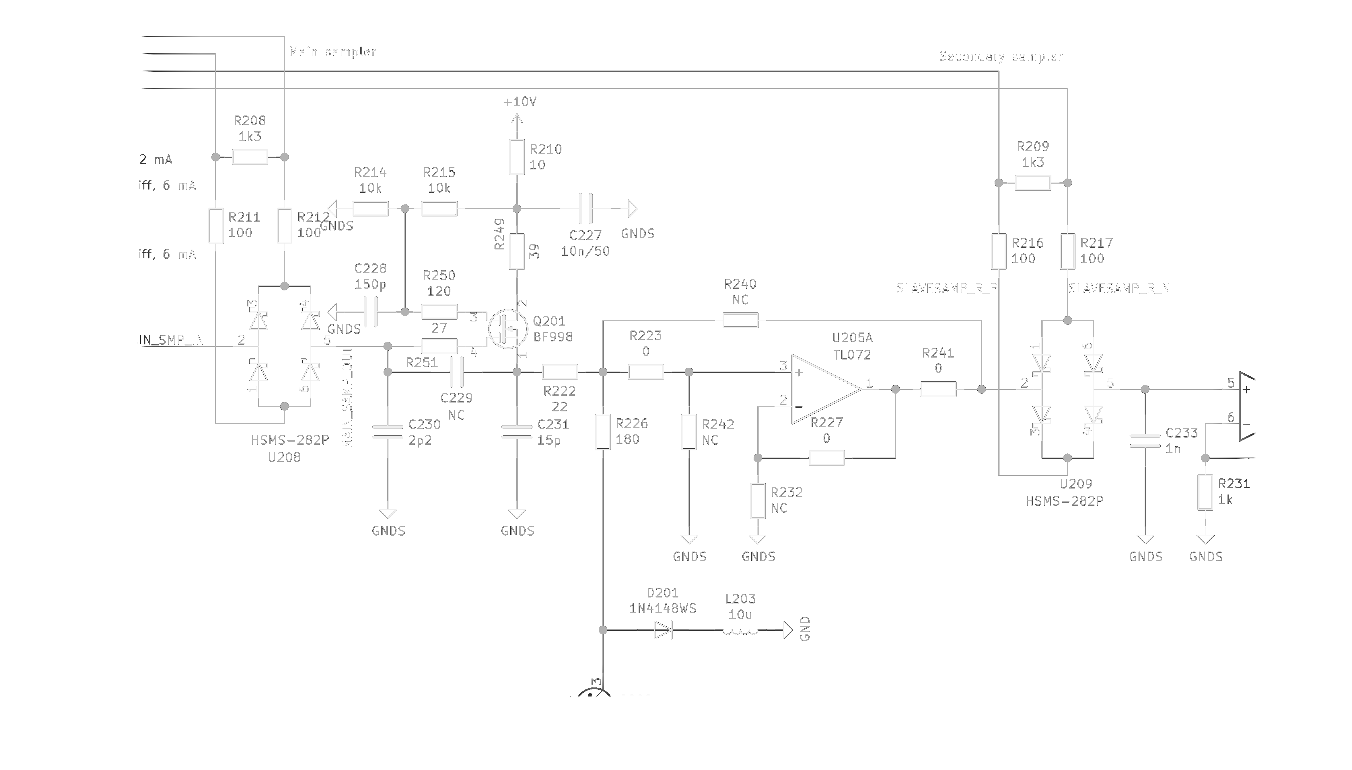
To fight with droop, my reflectometer uses BF998 MOS tetrode as input amplifier followed by second sampler section with much larger sampling capacitor (1 nF). These two samplers are precisely synchronised. The output of the second sampler is then measured by ADC. There is one slight error, the C231 in source of the tetrode is not used in the final reflectometer. It would make the amplifier unstable or make it oscillate. The same would happen if the C230 was larger, R251 was smaller and so on. The circuit is tuned to be as fast as possible while being stable. Making the C230 larger also loads the sampling bridge much more and causes the input impedance of the instrument drop at higher frequencies. Since the bonding wires of the sampling bridge are inductive, the sampling bridge forms a resonator with the C230.
![]()
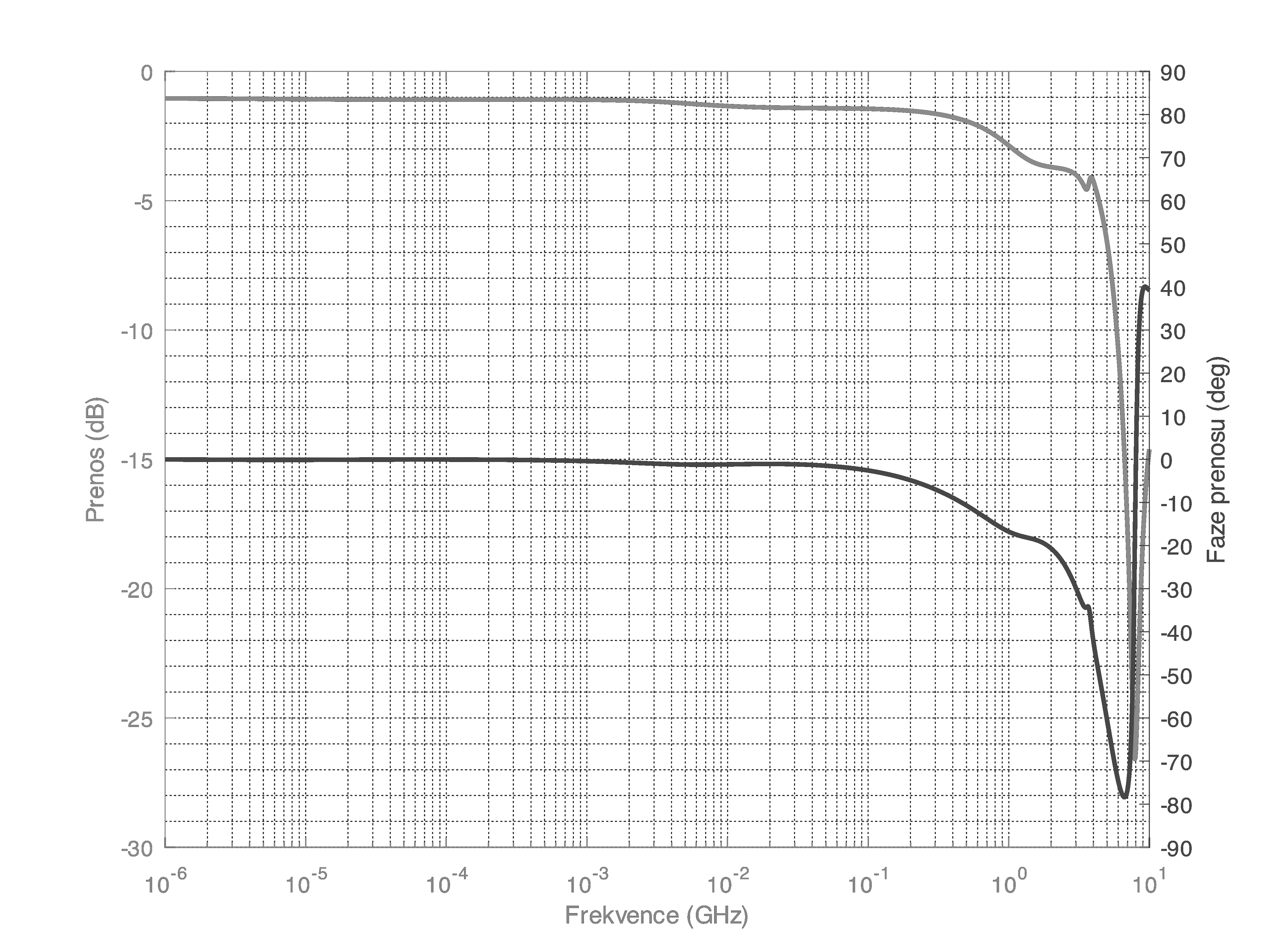
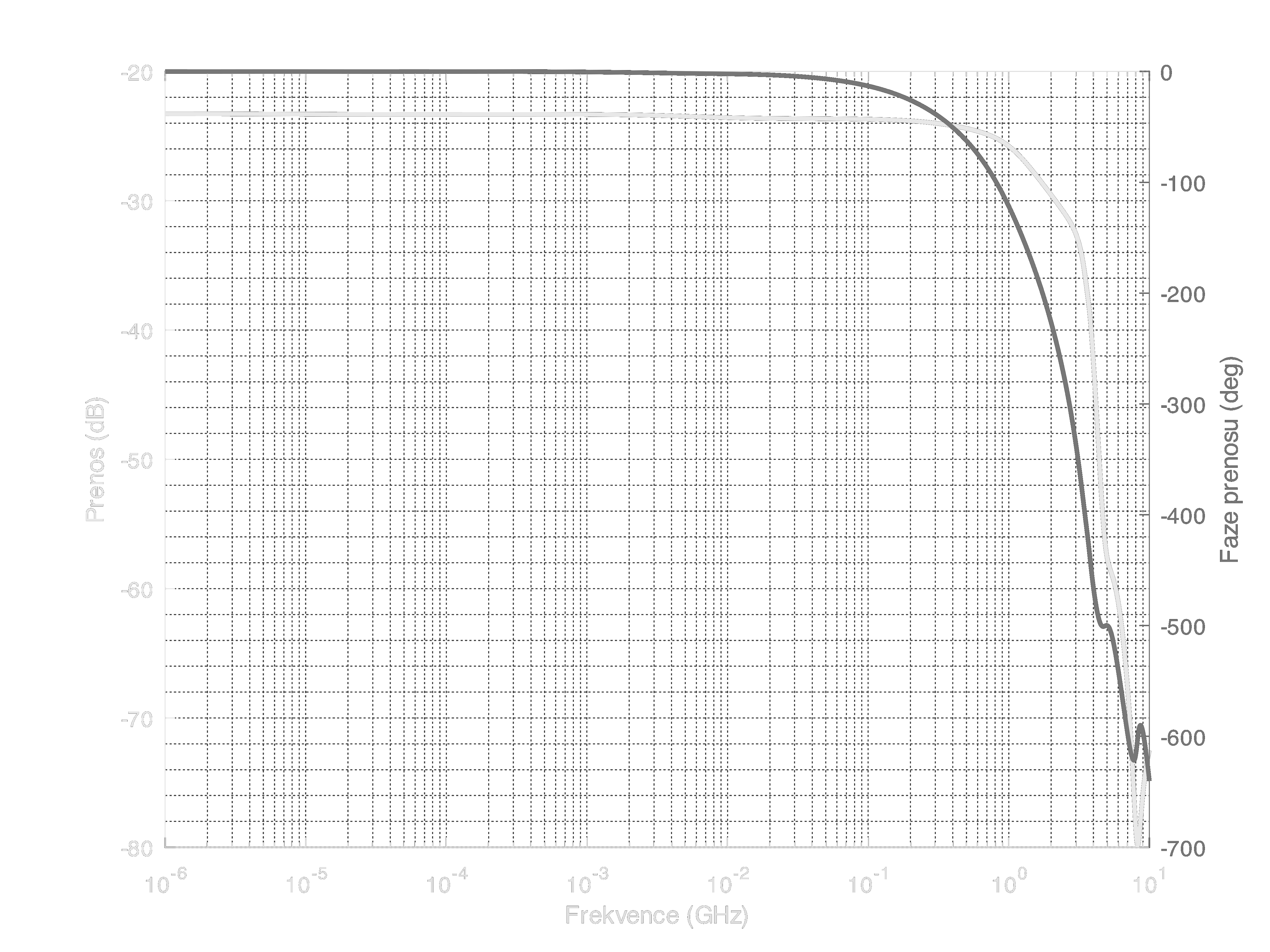
To explain why there are so many resistors and capacitors placed in seemingly strange places, have a look at the transfer function of the amplifier. Please note that the -6 dB corner frequency is predicted by simulation to be at about 4 GHz, while the transistor is recommended for applications under 1 GHz. Yes, it smells of some positive feedback. But carefully crafted not to turn into instability. Sorry for the captions in graph being in Czech, the bright trace is S21 parameter.
![]()
The transfer function of the whole sampler, from test connector to the output of the BF998 should look somewhat like the next image. According to simulations, the -6 dB corner frequency should be near 2 GHz. To repeat a currently common cliché, "not good not terrible". If you want more bandwidth, you have to come up with a better strobe driver than a LVCMOS outputs with series resistors, for example one of those Tektronix ones from previous log. And a better buffer amplifier. However note that these graphs are from simulation which was performed for the case when the sampler is in the "track" mode. In reality, it is possible to measure faster risetime than predicted by these graphs, because the graphs do not take into account the characteristics of the sampler during the transition to "hold" state and the behaviour of the circuits after that event. Of course, it could be worse as well in reality.
![]()
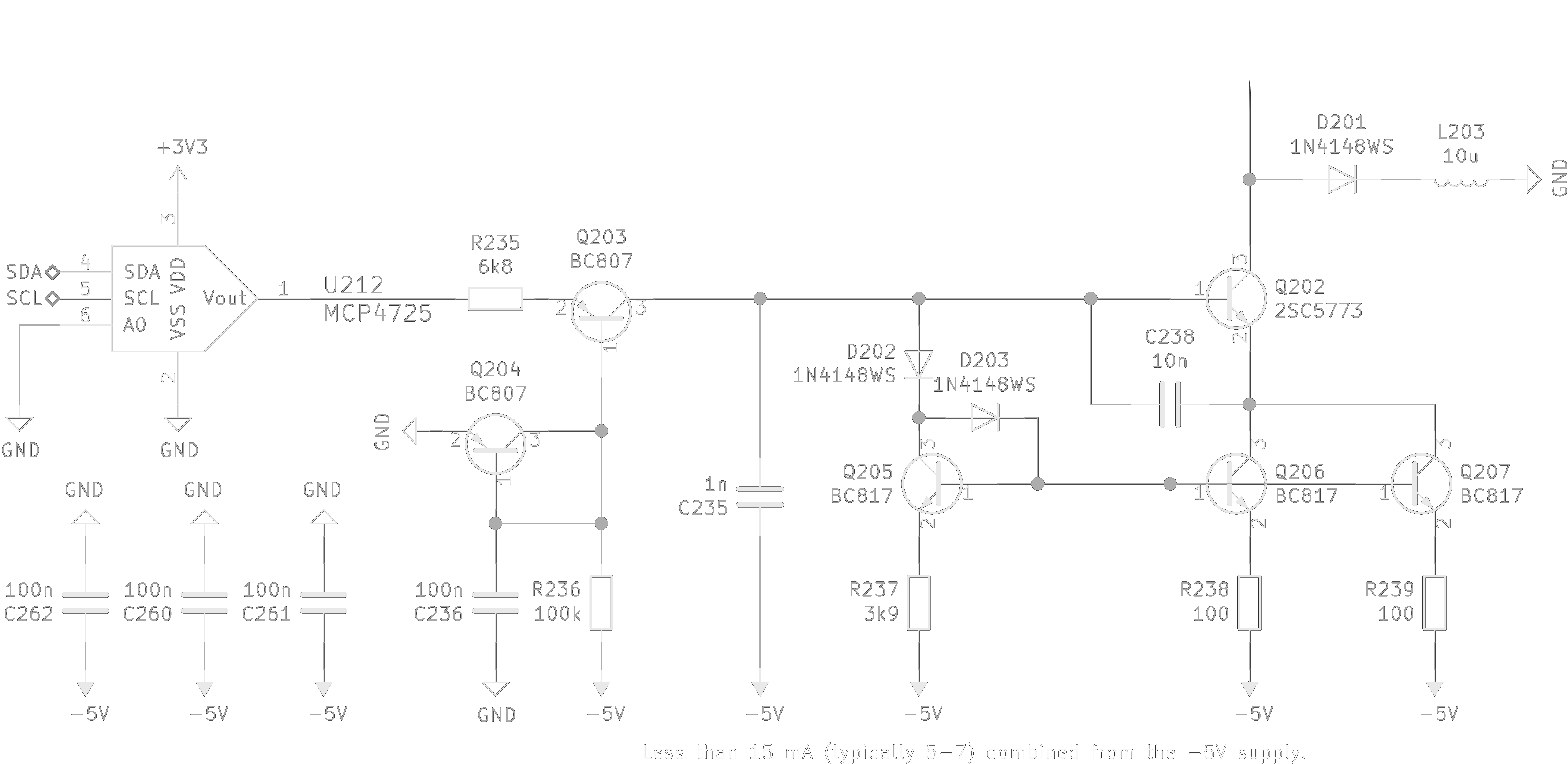
To reduce distortion and increase input impedance of the BF998, a current source is used in its source terminal. The current can be set from 0 to about 12 mA using the DAC. This facility is used for autocalibration of the amplifier, because the BF998 has large manufacturing tolerances, so this cicuitry allows to tune the DC offset of the measurements.
![]()
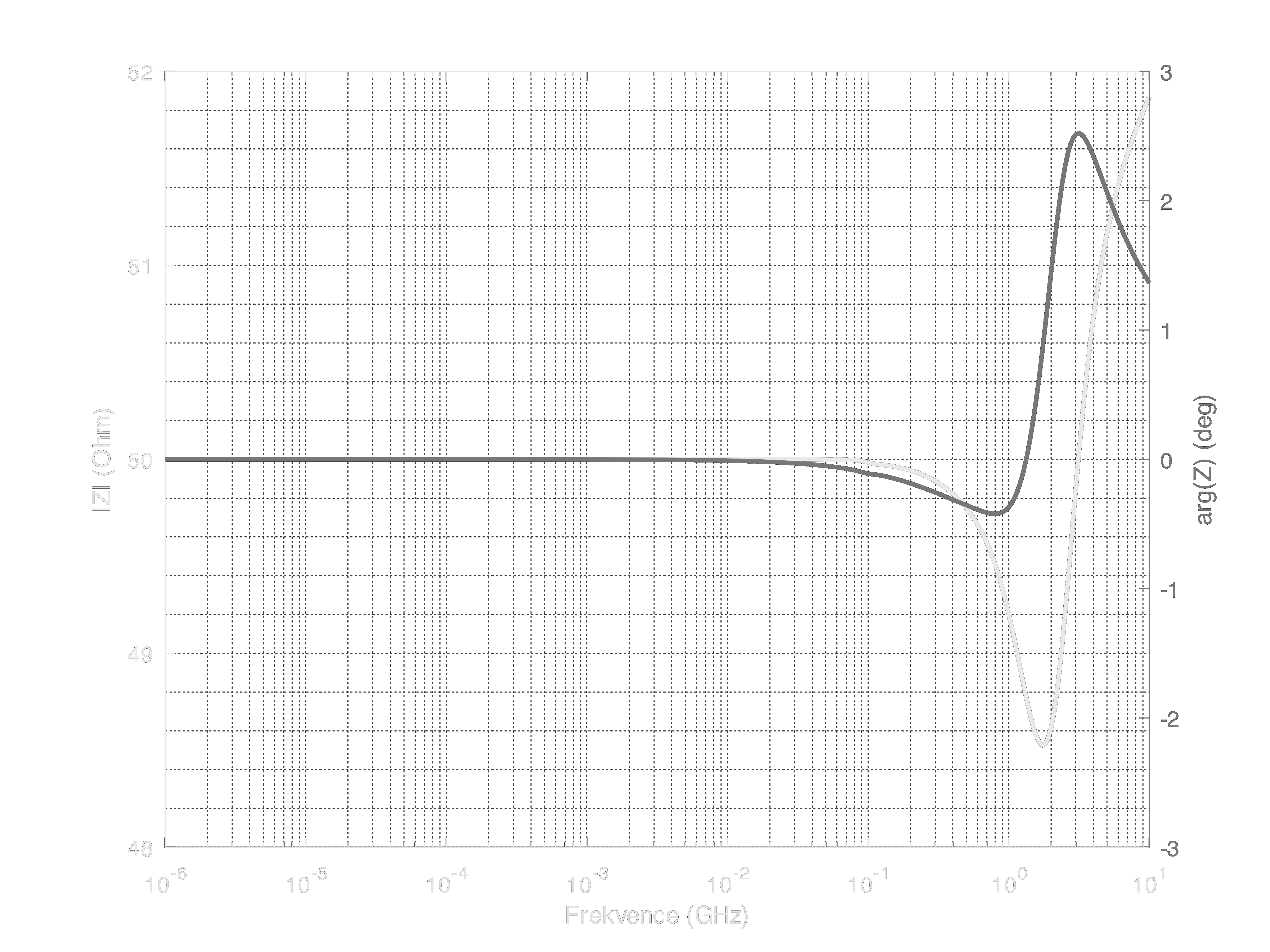
If you are curious about the input impedance of the instrument, you can find it on the next graph.
![]()
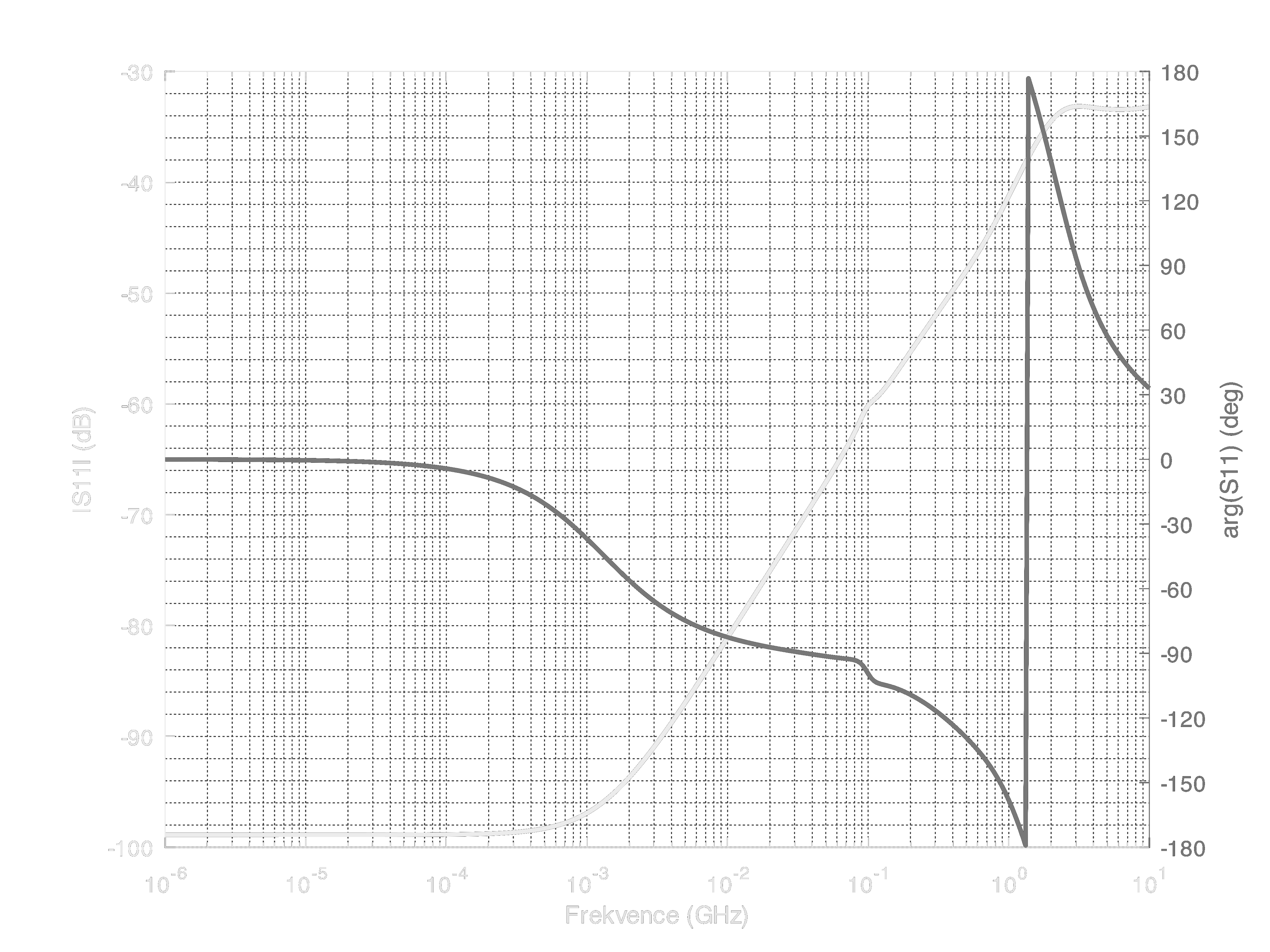
If you would like more to see the input reflection coefficient, the next graph could suit your curiosity. Of course, it is only hypothetical and based on simulation. You can see the resonance of the sampling bridge between 1 and 2 GHz.
![]()
Next time, I will probably write about the pulse generator.
-
How to sample fast while keeping your wallet safe
01/10/2020 at 17:23 • 0 commentsHave you ever had the need to sample some analog signal? If so, it was probably at low frequencies. Quite probably some audio grade stuff. Everyone knows how to do that. Either take a complete sample-and-hold amplifier like the old LF398 or the DIY way by connecting together some generic amplifier, capacitor and some electronically controlled switch like the 4066.
But what if you look a bit higher? Several megahertz and up? Okay, the 4066 method still may be useable. You can find quite a lot of receivers which use a 4053 or 4066 as an IQ demodulator for short-wave amateur radio. Still good, still cheap and simple.
![]()
![]()
But the true question is what happens once you want to sample something which extends beyond several hundred megahertz or even several gigahertz. Then you will find yourself in a very uncomfortable place. If you wish to do some voodoo with OTAs, you can reach hundreds of megahertz, but for more you have to dive into your pocket and look very deep in your pocket. First, you will be shocked because there are only a few parts which can do such things, like the HMC760. But seriously, are you going to pay $360 for a chip? Maybe, but not me.
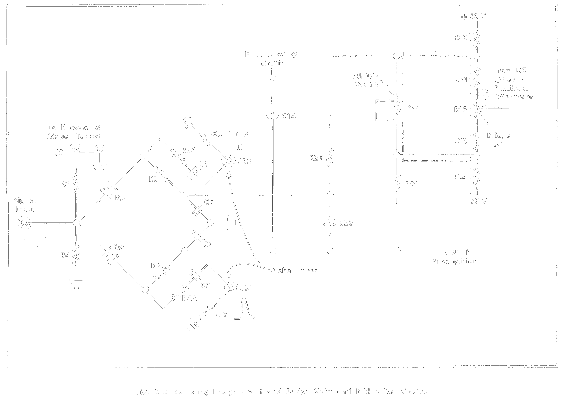
Okay, so searching at e-shops answered the question showed us there is no part which would do this job for us. Time for diving into old manuals, schematics and articles! Maybe some of you have already met some old TDR machine or a 60s Tektronix sampling oscilloscope. They usually have quite similar sampler. Some are very simple, some are very intricate. But the principle is always the same - using diodes as sampling bridges. When current passes through them, so does signal. Turn off the current and the signal also stops going through. Ideally, that is.
![]()
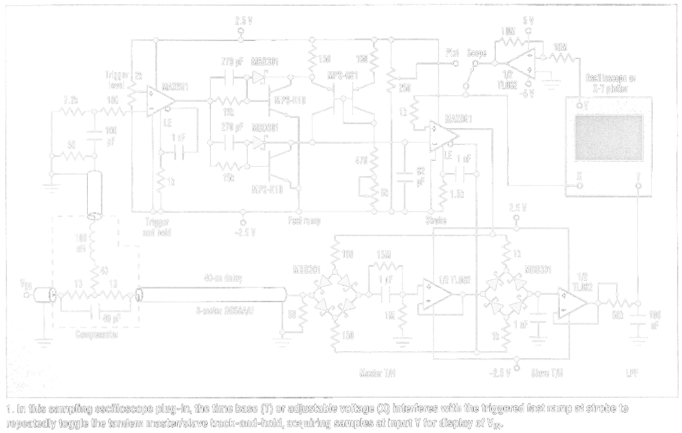
What you can see on this part of schematic form S-2 sampling head is the sampler. It doesn't look obvious, does it? If you don't believe it is a sampler, read the manual which explains the whole sampling head and each of its parts, how it works and how to make it work. It's sad you don't get a manual like this these days. Note that this sampling head was introduced in 1967 and offered 4.6 GHz of bandwidth and <75 ps of risetime.
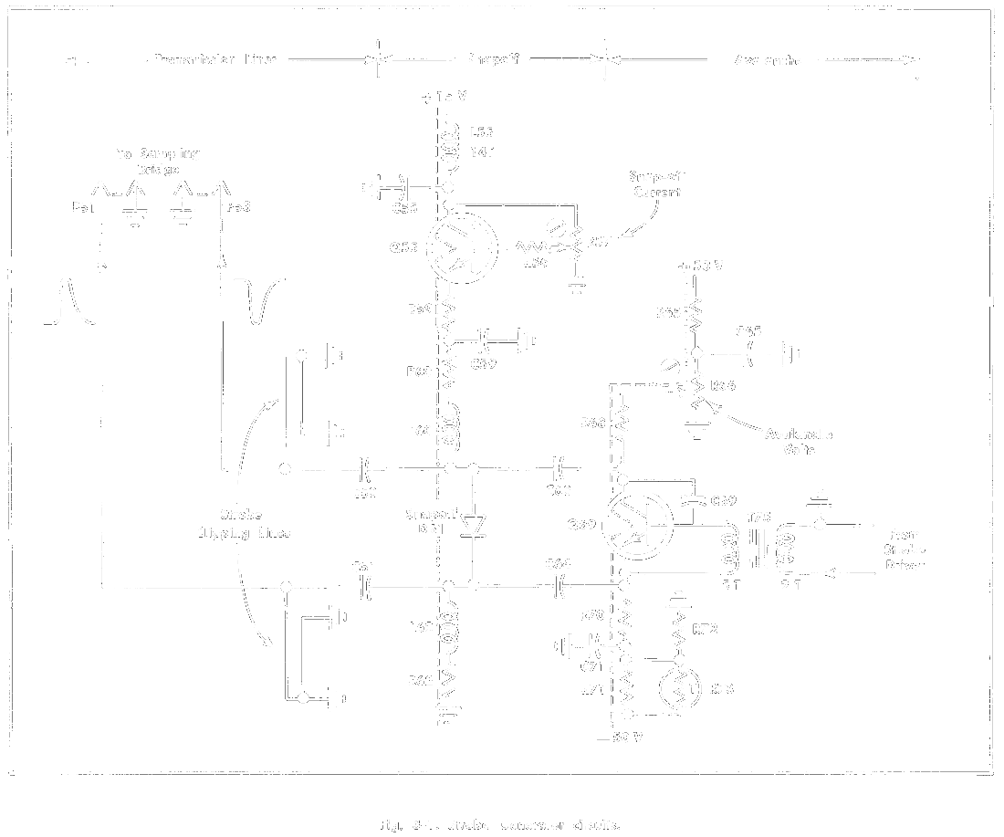
To summarize it: a very short pulse of current of defined length goes through the diodes, turns them on briefly and then turns them off again very fast. The two key parameters here are how fast you can turn off the diodes and how precisely you can control at what time it happens. Let's look at how the folks at Tek did this magic.
![]()
What you see is an avalanche pulse generator. You may have already seen it in one of my projects. Essentially it is transistor which has collector-emitter voltage so high it almost goes into avalanche breakdown, but not on its own. The avalanche is triggered by other circuitry using the transformer on the right. This makes a very fast pulse. To make it even faster, a snapoff diode is used (these are very hard to come by these days). The length of the pulse is precisely set by the two "cliplines" on the left.
It is fast and great, but it requires several supply voltages (and quite high!), draws a lot of current and cannot be triggered very often, because it has to reach steady state again. What about doing it less complicated?
If you look at article by Hubert Houtman, you can see that it is possible to achieve about 1 GHz of bandwidth using just a "quite" fast comparator and two resistors.
![]()
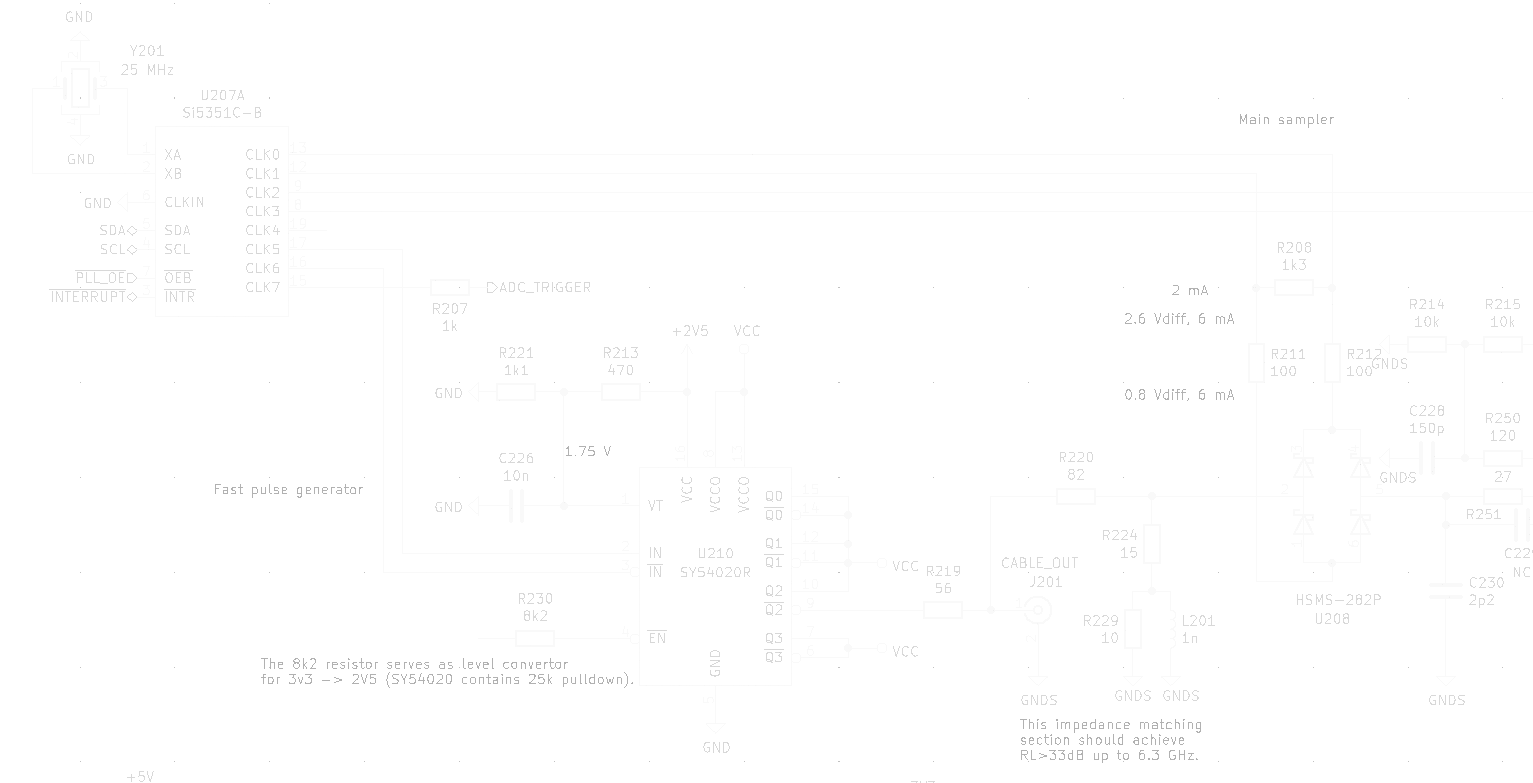
The MAX961 comparators have rise/fall times about 2.3 ns. The outputs of the Si5351 have those times under 1 ns and are implemented as current sources. Theoretically, this could get us at least 2 GHz of bandwidth using the same diodes. Since we can get faster diodes today, it could be even better. The only unpleasant side effect is a need for a virtual analog ground at 1.65 V potential (half the 3.3 V supply for the Si5351).
To see how simple it can be, look at the lower right part of the next image. Four diodes, three resistors and directly connect it to Si5351. Nothing complicated. The result is about 200 ps of measured risetime from generator with 85 ps risetime.
![]()
-
Equivalent-time sampling is the key to cheap reflectometer
01/10/2020 at 14:47 • 0 commentsWhen I was designing this TDR, I was trying to avoid using expensive parts. Thus, ECL delay lines were out of question. I found a few articles which were using other ways to achieve equivalent-time sampling.
For example, there was a project which used two oscillators which were slightly out of tune. The problem was that it was highly "academic". The time step was dependent on the frequency of those two free-running oscillators, thus it depended on temperature, supply voltage and moon phase. Good idea, but not useable in such form. See the original article on IEEE XPlore (or look it up using SciHub or Library Genesis if you do not have access to scientific articles) A 16ps-resolution Random Equivalent Sampling circuit for TDR utilizing a Vernier time delay generation.
There were also several projects which used FPGA which implemented a DDS. This DDS generated a sinewave whose phase could be arbitrarily set in very small steps. Then this sinewave was turned into square wave. This way, the researchers were able to generate pulses for generating a pulse for the TDR and sampling pulses in one FPGA and a handful of components. The sampling was performed by a fast latchable comparator. In my opinion, this is the best architecture of TDR which I have seen in scientific articles, however I wanted to avoid FPGAs. See Miniaturized FPGA-Based High-Resolution Time-Domain Reflectometer
Then there was project which utilized D-type registers in the FPGA to directly store a train of pulses. Very imprecise, temperature dependent and needs a re-evaluation each time you generate bitstream for the FPGA (yuck). I hate non-deterministic digital circuits also, so this one was also out of question. See A Time Domain Reflectometer with 100 ps precision implemented in a cost-effective FPGA for the test of the KLOE-2 Inner Tracker readout anodes
Delay-line based reflectometers also turned up, however these are too expensive and too limited. See Sequential sampling time domain reflectometer
And then there was the usual bag of sh** which you can find in scientific articles, usually from universities which have to publish articles, even though they have nothing to show. This usually revolves around connecting pulse generator to oscilloscope, several pages of description of the splitter used for connecting together the generator, oscilloscope and DUT, then several pages covered in equations describing everything from Maxwell equations to the effect of solar eclipse on price of donuts after Easter 1919.
And so it seemed I had to come up with something new (almost). I was playing with dual-VCO PLLs Si5351 at the time, so I thought if I could use them for this purpose. The answer was "probably yes, why not try it". And so I did. These PLLs allow you to set frequency of the two VCOs which can be non-integer. The fractional part allows the two frequencies to differ by less than 1 ppm. And the relation is precisely controlled as opposed to the "Vernier" article. So, nothing really new, just using newer and more interesting parts. When set to exactly 1 ppm difference in frequency, one can get one million of samples during one measurement cycle. I set the measurement cycle to 10 microseconds so it could be easily measured by internal ADC of STM32 microcontroller. This gives the ability to measure 1 million of samples 10 picosecond apart.
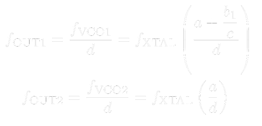
The frequency of the two VCOs is below, parameters a, b and c are the integer and fractional part of multiplier, d is the divider.
![]()
The time step of sampling is then given by the next equation:
![]()
From these equations, you can find out how to set the parameters to suit your needs (time step, number of points, measurement length).
Standalone digital TDR (TDR-G2)
My second generation TDR which aims to be standalone (no oscilloscope) and as cheap as possible while being usable.
 MS-BOSS

 Test port impedance
 Now, I think I have already exhausted all the interesting themes of this project, so I will probably stop writing logs about this project and we could move on to discussion in comments section.
 Forget about the spectrum above 11 GHz. The noise floor corresponds to "near-zero" values in floating-point computations during FFT. Simply said, it is the noise floor of floating point numbers. When you do something in floating point, stay aware of the fact that its precision is not infinite. There are cases when you might run into this issue and then you have to resort to arbitrary-precision mathematics which can be slow as hell.
 The resulting Wiener filter looks the like this.






 As you can see, it tries to detect the type of the discontinuity. It can detect "open", "short", "doubled impedance", "halved impedance" and for other cases it only shows "higher impedance" or "lower impedance".
 And it can even tell you if you are running the Octave binary from Flatpak with restricted access to serial ports and tells you how to correct it.
 After a handshake is performed, the GUI tells you the version of the firmware (time of compilation) and then finally connects to the reflectometer.
