John Lonergan
-
Using PROGMEM
02/07/2020 at 17:12 • 0 commentsMassive reduction in dynamic memory needs (IE ram) due to moving all strings to flash. Much more stable now.
Created a convenience library using macros for writing to serial.print as my old functions approach no longer works with the flash strings.
-
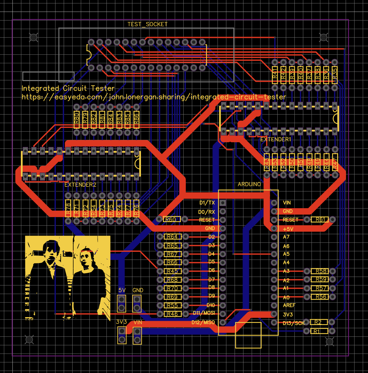
Minor PCB rework
02/04/2020 at 12:47 • 0 commentsI reworked the board to allow for a wide ZIF socket as there are wide "universal" Zif sockets that allow 0.3 and 0.6 chips giving more versatility.
Also corrected a hardware error where I had mistakenly taken INTA and INTB on the MCP23017 as inputs rather than outputs. The previous hardware tied these to Vcc using a 10k resistor. The earlier revision of the board seems to work in practice despite this, however now I've left these INT outputs as unconnected.
Also, I didn't like the way that the layout software was working so I made a minor mod. My PCB has wide power tracks and in some cases I have MCP23017 contol lines tied to Vcc or Gnd and this meant the fat trace came right up to those pins which cluttered the layout and caused clearance problems. So I included a 0ohm resistor in front of those pins to terminate the layout rule and drop back to a narrow trace. In the finished product this will be a jumper. Perhaps I could have done the same by using pad to separate the two traces? Anyway, now I have no problems with clearances.
-
Why didn't I get a better ZIF socket?
02/03/2020 at 11:00 • 0 commentsThe socket I have can hold only narrow (0.3) chips.
There are sockets out there that will hold both narrow and wide (0.6) chips.
This would have allowed me to test my wide pinned 7 segment LED's, or memory chips, as well as 7400 logic.
Another thing learned I guess.
-
Visual inspection of LED Array
02/03/2020 at 10:51 • 0 comments -
Example Log Output
02/03/2020 at 03:41 • 0 commentsSuccessful test example:
Testing: 74245 : Transceiver 8 bit
PASS  : -XZZZZZZZZGZZZZZZZZ1V- : OE disabled
Result: -_........_........__- : OE disabled
PASS  : -100000000GLLLLLLLL0V- : A to B all low
Result: -__________........__- : A to B all low
PASS  : -111111111GHHHHHHHH0V- : A to B all high
Result: -__________........__- : A to B all high
PASS  : -0LLLLLLLLG000000000V- : B to A all low
Result: -_........___________- : B to A all low
PASS  : -0HHHHHHHHG111111110V- : B to A all high
Result: -_........___________- : B to A all high
matches 74245 -
Now supports 3rd party chip defs
02/03/2020 at 03:33 • 5 commentsCan now import chip defs from Smart-Ic-Tester using a utility (python) that translates the database.txt file into C code as a collection of #defines.
My project cannot use the raw database.txt file directly as the Arduino Nano I used doesn't have a file system.
(Frankly the Arduino's lack of memory is also annoying me a bit).
-
What I've Learned So Far
02/01/2020 at 02:44 • 0 commentsVoltage Levels
- HC logic chips data sheets say VCC may be as low as 2v typically
- HCT data sheets quote 4.5v as lowest Vcc but this is merely the min in order to maintain TTL compatibility. In reality HCT will run fine at lower Vcc.
- LS will also run at lower voltages. See http://www.ti.com/lit/an/sdya009c/sdya009c.pdf - _Texas Instruments - Designing With Logic_ Section 2.2 Behavior With Low Supply Voltages: _"TTL devices attain stability with a supply voltage of about 3.5v, and are fully functional at a typical voltage of 4v"_
HC/HCT/LS will all run fine at lever voltages than 5v. This is handly because there will be a voltage drops below 5v when powering and driving the test chips from the GPIO pins.
On the Zif socket I measured a voltage of 4.7v-4.8v with a 5v supply. This voltage drop was less than I expected. - The MCP23017 extender documents a high level output voltage of Vdd-0.7v, but perhaps thats a conservative value or perhaps I was measuring test pins driven by the Arduino...- The ATmega328P documentation guarantees a high of at between 4.7v and 4.8v on a 5v supply at 10mA load. 2mA would be 4.9v or more. See page http://ww1.microchip.com/downloads/en/DeviceDoc/Atmel-7810-Automotive-Microcontrollers-ATmega328P_Datasheet.pdf "Figure 29-10. I/O Pin Output Voltage versus Source Current"
In anycase it's convenient that I'm seeing reasonable voltages on the Zif vs the needs of the various logic families.
EasyEda
- Its fun
- Its time sink
- The power and ground lines should be made wider than defaults - use design rules - Tweak the default track separation and track width so they are more robust and lower resistance - use design rules
- Check the design rules violations list for clearance errors before committing
Arduino Nano
- There is sufficient capacitance on the GPIO pins and lines out to the Zif socket that writing to a disconected pin (empty Zif) and then reading that same pin returns the logic level that was previously written, rather than a random value. See below for more information.
- The analog A6/A7 lines cannot be used as digital outputs, just digital inputs only
- The I2C pins SCL/SDA are open collector and need pull ups - but see more below
- D13 is connected via a 1k resistor and an LED to ground so this can interfere with it's reliability as a digital input due to the pull down. IF it is to be used at al then it is intended to be used as an output. - The header pins supplied with the Elegoo Arduino nano don't fit in a round pin DIP socket and the header pins are made of a metal that doesn't solder easily
- There is a lot of confusing discussion on whether one needs to add pullups to the I2C bus lines
So, do I or don't I need pullup resistors on the I2C lines SDA/SCL?
There is a lot of confusing info on this online.
Firstly, I found this explanation of why some kind of pullup MUST be present .... - "I2C bus drivers are "open drain", meaning that they can pull the corresponding signal line low, but cannot drive it high. Thus, there can be no bus contention where one device is trying to drive the line high while another tries to pull it low, eliminating the potential for damage to the drivers or excessive power dissipation in the system. Each signal line MUST HAVE a pull-up resistor on it, to restore the signal to high when no device is asserting it low."
However, the I2C pins on the Ardunio have built-in optional pull-up resistors. Fortunately, the "Wire library" turns on the internal pull up resistors in it's twi_init() called by Wire.begin() function on SDA & SCL. Doing this puts a weak-pull up on the I2C pins even though they are acting as outputs. Further digging explains that it is possible to have these digital input pull-ups turned on despite the pins acting as I2C outputs because the digital IO circuitry that contains the pull-up is in parallel to the I2C IO circuitry so they are not exclusive. Convenient!
And, for a physically short bus and where the voltages on each end are the same then a design doesn't need additional external pullups on the I2C pins.
Stray Capacitance test result
I tested what would happen if I left the Zif socket empty then set the GPIO as output and wrote a 1's to all the pins. I then turned the pins into inputs and measured the logic level every few seconds to to see what unfolded.
I've included the test results for my soldered PCB below.Testcase : 1111111111111111111111 Result : -1111111111111111111111- : 0 secs Result : -1111111111111111111111- : 1 sec Result : -1101111111111111111111- : 2 secs Result : -0001111111111111111000- : 6 secs Result : -0000000000000110000000- : 10 secs Result : -0000000000000010000000- : 15 secs Result : -0000000000000010000000- : 20 secs Result : -0000000000000000000000- : 25 secs
Further run ...
Testcase :  1111111111111111111111
Result   : -1111111111111111111111- : 0 secs
Result   : -1111111111111111111111- : 1 sec
Result   : -1001111111111111111111- : 2 secs
Result   : -0001111111011111111000- : 6 secs
Result   : -0000000100000111000000- : 10 secs
Result   : -0000000000000010000000- : 15 secs
Result   : -0000000000000010000000- : 20 secs
Result   : -0000000000000010000000- : 25 secs
What I see is that reading the pins echo's back the logic levels that were written to them moments before. We can see that at time passes the memory decays and the pins gradually start reporting logic 0. This decay consistently takes around 25 seconds to complete.
Running this same test over and over I found that the same pattern of decay to 0 was consistent on each run. I guess this is a consequence of each path having it's own unique RC.
-
Stray Capacitance mystery solved?
02/01/2020 at 02:39 • 0 comments -
Stray Capacitance on the GPIO pins?
01/31/2020 at 02:51 • 2 commentsI wrote up some docs on what I've been seeing as strange results for stray capacitance on the GPIO pins. See "Stray Capacitance" in the GitHub README for full details.
I can't understand how the signal takes so long to decay - am I wrong about this being just RC from the pcb trace & zif socket? The RC would be tiny but the decay takes 25 secs.
?????
-
PCB arrived and assembled and now being extended
01/28/2020 at 02:42 • 0 commentsDesigned on EasyEda, sent PCB for making, soldered the components and tested a few chips.
I'm currently extending the software to include other's databases of chip tests.
![]()
Integrated Circuit Tester & Exploratory Tool
Interactive tester and exploratory tool for logic chips