Close
0%
0%

STM32F767 Development Board Upgrade

Upgrade the QSPI flash chip on a common EBay STM32F767 Development board

Similar projects worth following
On another project of mine, I'm trying to create an open STM32 TouchGFX capable minimum system. Eventually, it will migrate to a custom PCB but to get started, I'm using off the shelf development boards and breakout boards. And one of them can use an upgrade to make things a little easier. Read on!

TouchGFX requires a handful of micro-controller peripherals, and a couple that aren't requirements, but become almost necessary as your GUI projects become more complex. One of those components is memory-mapped QSPI flash. This is used to store graphical assets to be copied to a frame buffer and then rendered to a display.

In my quest to create a minimum system, I've chosen a popular Ebay STM32F767 board as a starting point. It has a micro with necessary peripherals, an SDRAM chip and a QSPI flash chip. However, the mounted flash device (W25Q128) doesn't have an external loader for ST-LINK. So this project will upgrade it to one that does.

TouchGFX (and many other graphics libraries) will use some sort of flash memory to store graphics assets.  These assets could be images, buttons, fonts, etc.  Sometimes NAND based flash is used and sometimes NOR based flash is used.  TouchGFX by default looks for memory mapped flash memory and this is done on STM32 platforms through QSPI (Quad SPI).  This allows for a memory device anywhere from 1Mbit to 1Gbit in size to be connected with only a few pins and appear as "internal memory" to the micro-controller.  The data stored in this device has to be preloaded and available to the graphics application as soon as it starts.  In STM32 based platforms this can be done through the concept on an "external loader".  An external loader is some code compiled for the micro-controller that the debugger/programmer tool loads into RAM that then in turn loads data onto the attached memory device.  Writing one of these external loaders is not a trivial task, so it's much easier to leverage already proven ones.  The QSPI flash chip mounted on my STM32F767 is a Winbond W25Q128 and that doesn't have support in the ST-LINK debugger programmer.  So an upgrade is in order!

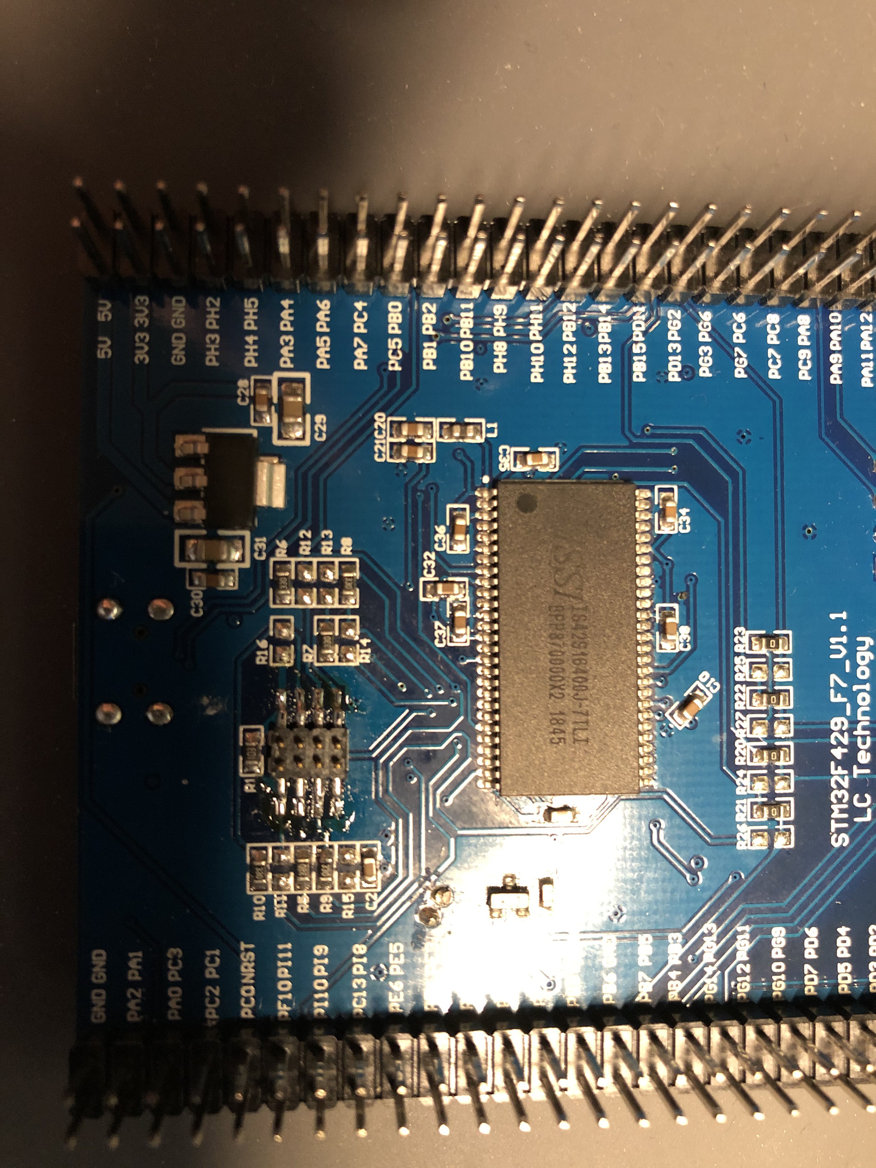
First, I'll describe the development board a little.  You can find this board on the likes of EBay or Aliexpress for around 25USD and it looks a little like this:
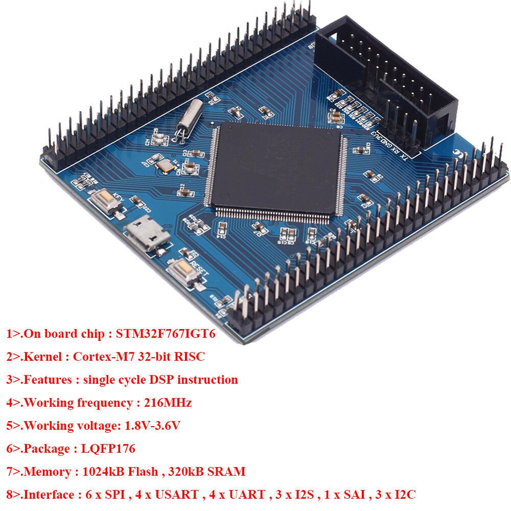
It has a beefy STM32F767IGT6 micro-controller, an 8MB SDRAM device and the 16MB flash device in question.
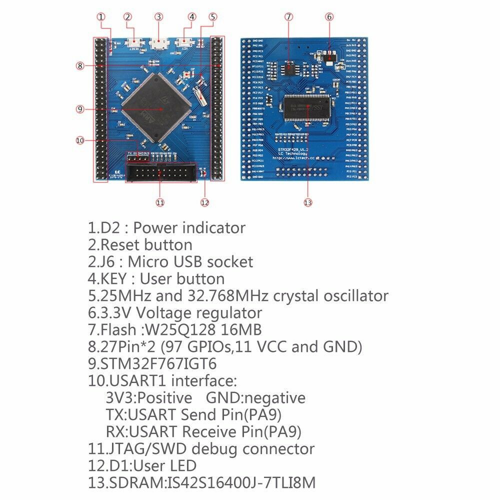
This upgrade will involve removing the flash chip, replacing it with pin header, designing and building a board with a bigger, more compatible QSPI flash chip and putting it together and testing it.

Since the flash chip is an SOIC-8 with 1.27mm pin pitch, I'm going to mount an SMD 2x4 1.27mm pin header to the pads of the flash chips PCB footprint.  I'll lay out a board in KiCAD that has an MT25QL512 on it.  The MT25QL512 has an external loader already built in to the STM32 tools.  In theory, this should all work wonderfully.

  • PCB Layout

    Andy02/05/2020 at 04:41 0 comments

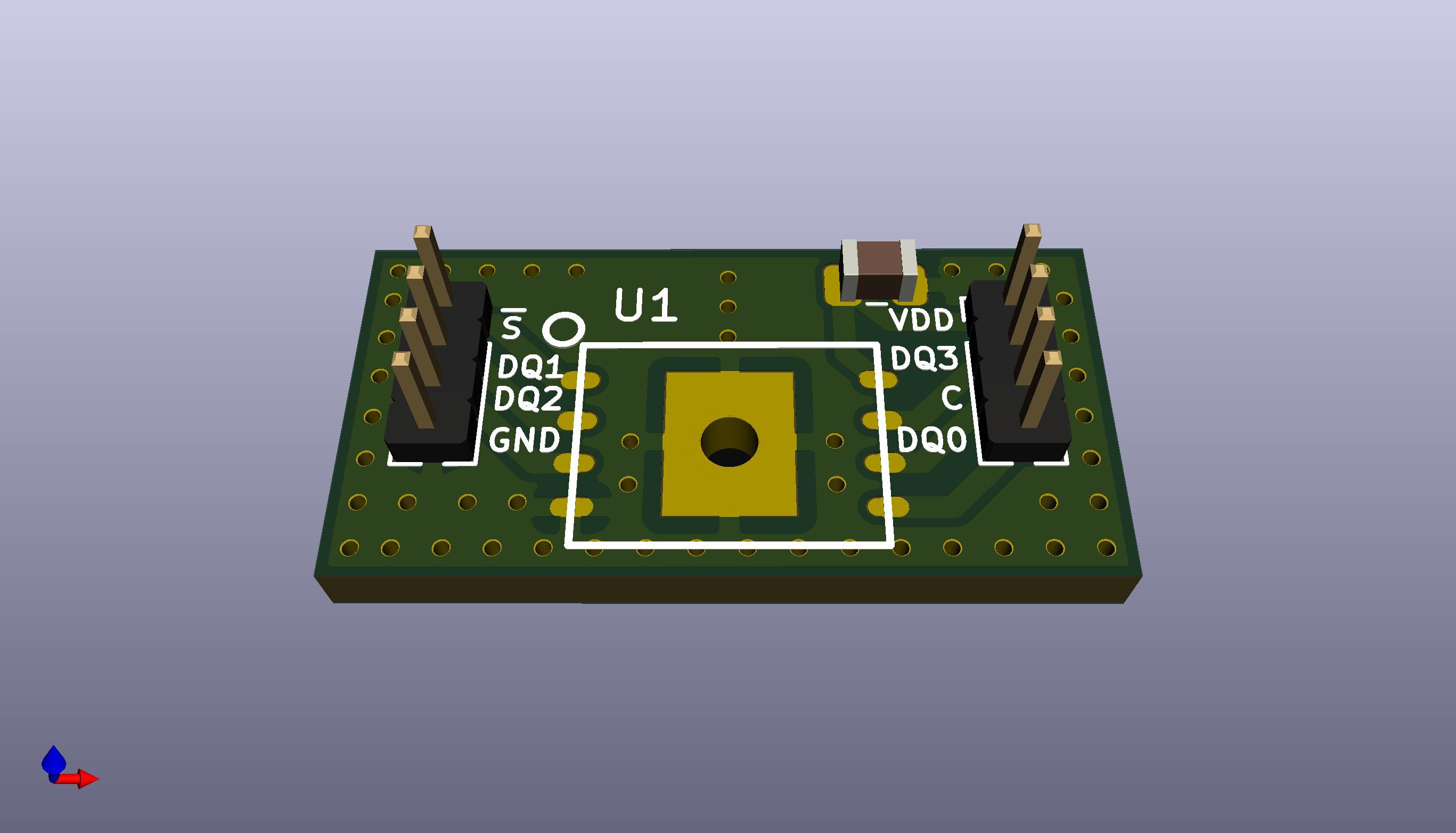
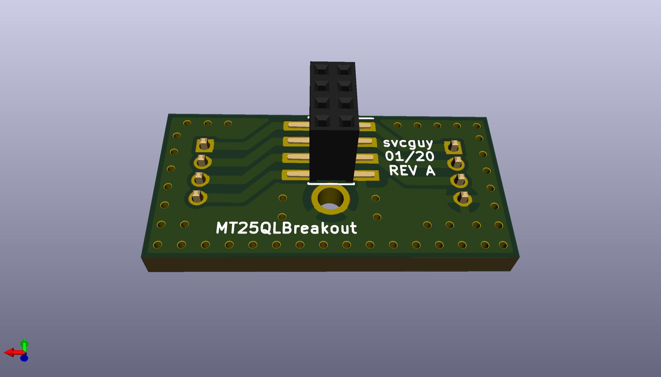
    The board to design is really simple and straightforward.  I'm going to put down a footprint for the MT25QL512ABB and an 0805 capacitor.  The bottom will have the 2x4 1.27mm SMD female socket.  Also by adding some 1x4 1.27mm pin header on each side this guy could double as a tiny general purpose MT25QL breakout.  The WPDFN-8 footprint is not included in the KiCAD library, but I already one that I had made from a project past.  SnapEDA has one, but I've not tested it, so YMMV.  All in all it's an incredibly easy board to lay out the only thing worth mentioning is that since the WPDFN-8 has a large EP pad on the bottom, I added a large via to that pad that will allow me to flow some solder under there to ensure a good thermal and electrical connection.  The board is tiny and even with OSHPark's Super Swift service, it only costs 3.20USD delivered!  Here's what the render of the board looks like:

    The Samtech female connector will be much shorter than pictured here.

    Here's the BOM

    U1 - MT25QL512ABB Digikey 557-1786-ND

    C1 - 0805 0.1uF 16V X7R (any will do) (not strictly necessary)

    J2 (bottom connector) - Digikey SAM13109CT-ND

    J1, J3 (top pin header) - Digikey 952-3600-ND (not necessary)

    Mating connector for J2 - Digikey SAM13898CT-ND

    Here's the board file on OSHPark:

    Order from OSH Park

    Next up, build it when everything comes in!

  • W25Q128 Removal

    Andy02/05/2020 at 04:13 0 comments

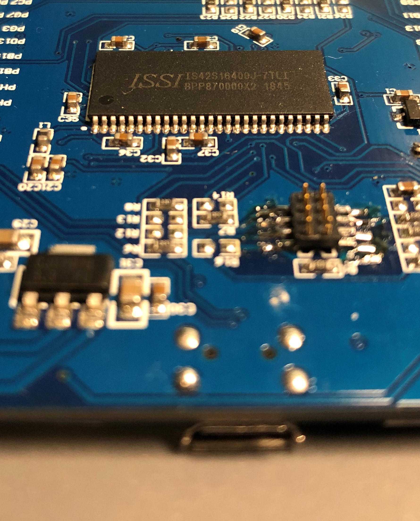
    The first step is to remove the existing W25Q128 flash device and replace it with some pin header to connect up a custom board.  The 1.27mm pitch SOIC-8 package is pretty easy to remove.  First start by cutting each of the eight pins with a pair of sharp flush cutters.  Then fire up the soldering iron and bits left over by heating them up and swiping them off.  Careful not to heat up the pads to much because you can lift them if you're not careful.  I selected the Samtech FTS header because the width of it matched what I expected the distance to be between the 2 rows of pads for the SOIC8.  The Samtech FTS-104-03-F-DV-TR can be found on Digikey (P/N SAM13898CT-ND).  After removing the leftovers of the flash chip, clean off the pads with some solder wick and tin one of the corner pads.  Line up the connector and tack it down onto that tinned pad.  Tack down the opposite corner and if everything lines up solder the remaining pins.  When you're done you should have something like this:

    Next step is design and build a board to mount there

View all 2 project logs

Enjoy this project?

Share

Discussions

KISHAN JOSHI wrote 10/06/2020 at 18:21 point

Great! can you provide some schematic for refrence ?

  Are you sure? yes | no

aiaisir wrote 02/26/2020 at 00:16 point

Thank you.

You gave me an easy way.

  Are you sure? yes | no

Similar Projects

Does this project spark your interest?

Become a member to follow this project and never miss any updates