Pascal
-
First testing: Mistake happens
05/17/2020 at 12:32 • 0 commentsOr how one should never trust existing footprint libraries without double and triple checking everything!
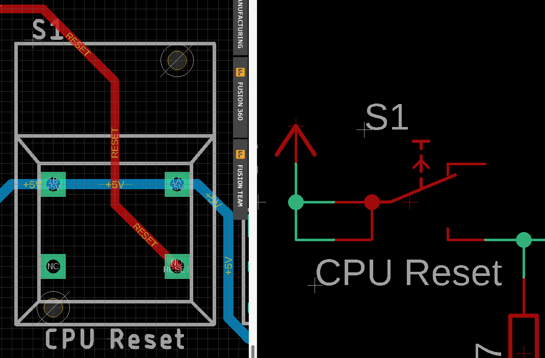
This morning I decided to finally test the Computer with all cards inserted and... no clock! Not only did I swapped X1 and X2 on the CPU board, which was quickly fixed with a bit of copper and a sharp knife, but the CPU's Reset Line constantly was held high, at which the Clock Circuit of the CPU gets halted. After measuring a few times, checking the datasheet and the schematic of the switch, I found the reason why:
![]()
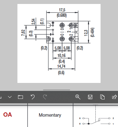
One would assume that the Reset Line is connected to 5V when the button is pressed. The footprint fitted perfectly to the switch I ordered on digikey, and even the symbol was nearly the same as in the datasheet. The only thing that I miss to check, and that could go wrong: Pins swapped!
![]()
In the actual datasheet, 2 and 0 are by default connected. Sadly the default library I found for it (Part "5501" in library "switch") has Pin 1 and 2 swapped.
I have to admit, that I rushed the creation of these PCBs a little, as I guessed that with the current COVID situation, shipping would get worse from China. In the hope to safe time by using as many existing libraries and parts, mistakes happend. Time to fix all 4 Buttons/Switches, but after that everything should work. Depending on the amount of errors, there will be a revision B at some point.
-
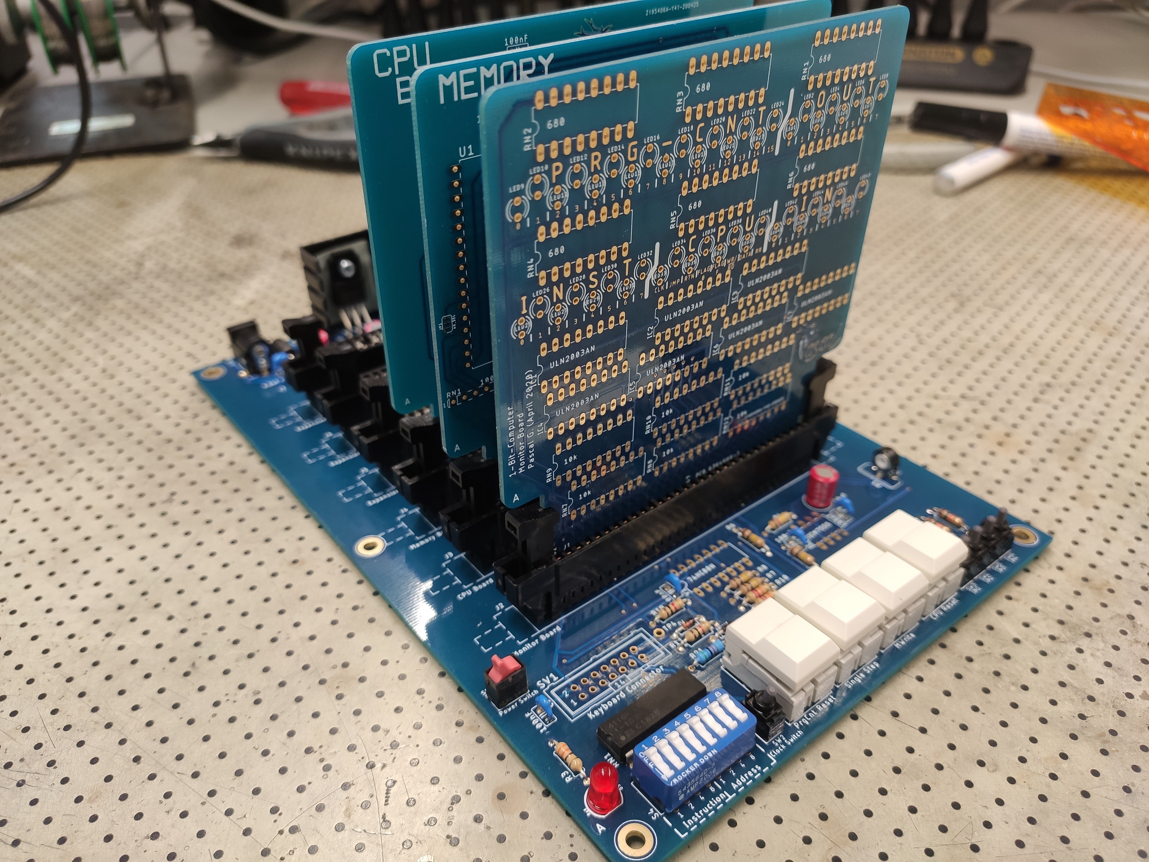
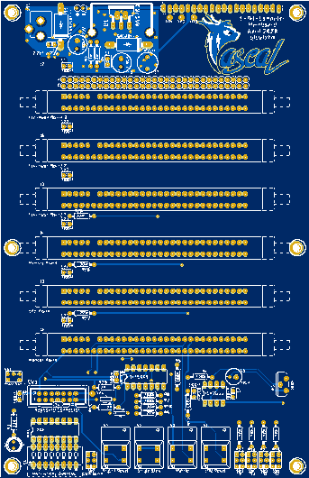
Assembly done
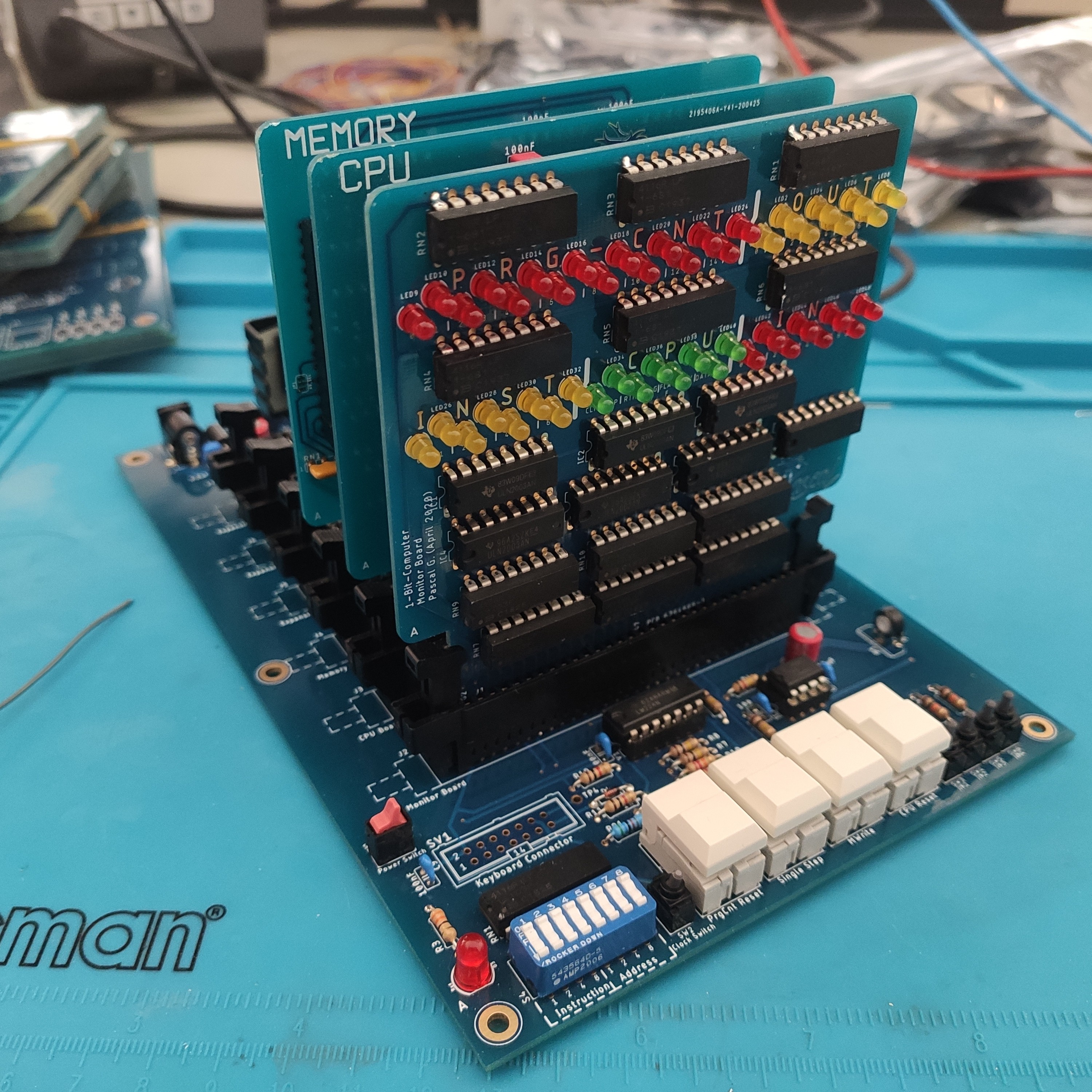
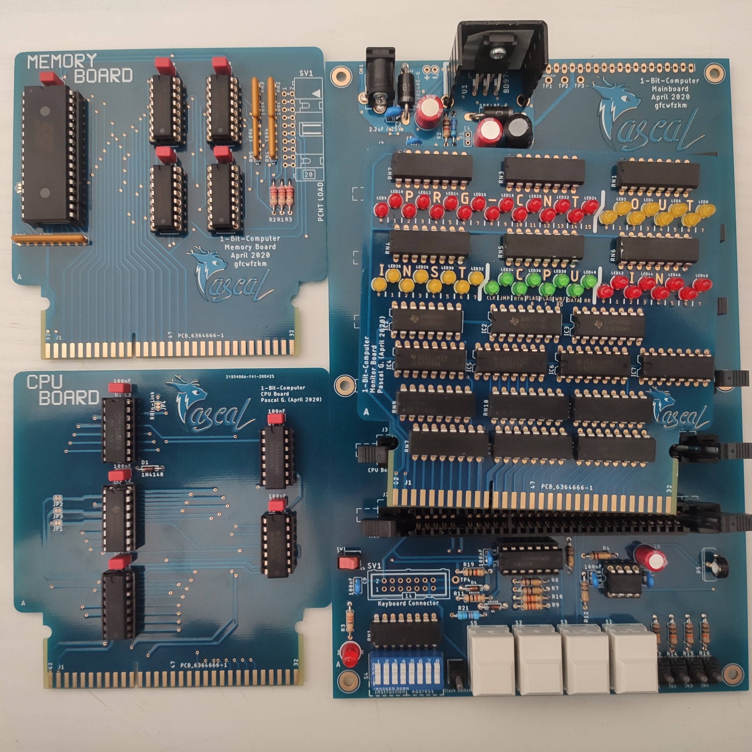
05/12/2020 at 15:50 • 0 commentsFinally all boards have been fully assembled and powered-on individually to check if any of them are faulty - so far, so good! The next step will be to test them on the main board, enter basic commands and see if it's running. Here are the pictures so far:
![]()
![]()
-
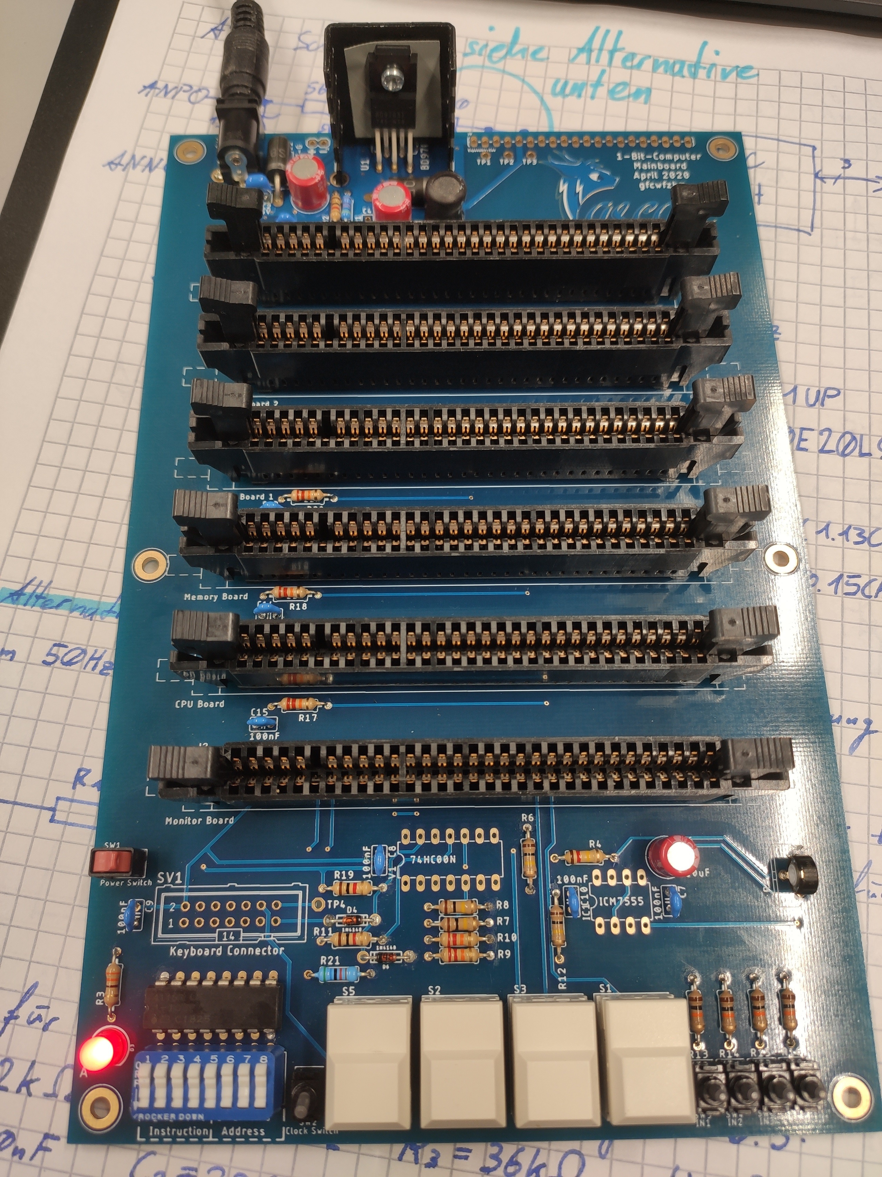
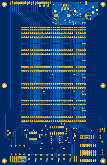
PCBs arrived & Mainboard assembled
05/04/2020 at 17:40 • 0 commentsFinally the PCBs from china arrived, and that with a corona-bonus in the delivery costs (70$ instead of the usual 20$ on DHL)
But at least, the PCBs all look as expected:
![]()
![]()
![]()
![]()
Found some time to assemble and test the main board as well. The Buck Converter delivered 5.04V - good enough for 1 bit computer! To my surprise, the card-edge-connectors hold the single PCB Modules better than expected as well, which were the only thing that worried me.
![]()
![]()
-
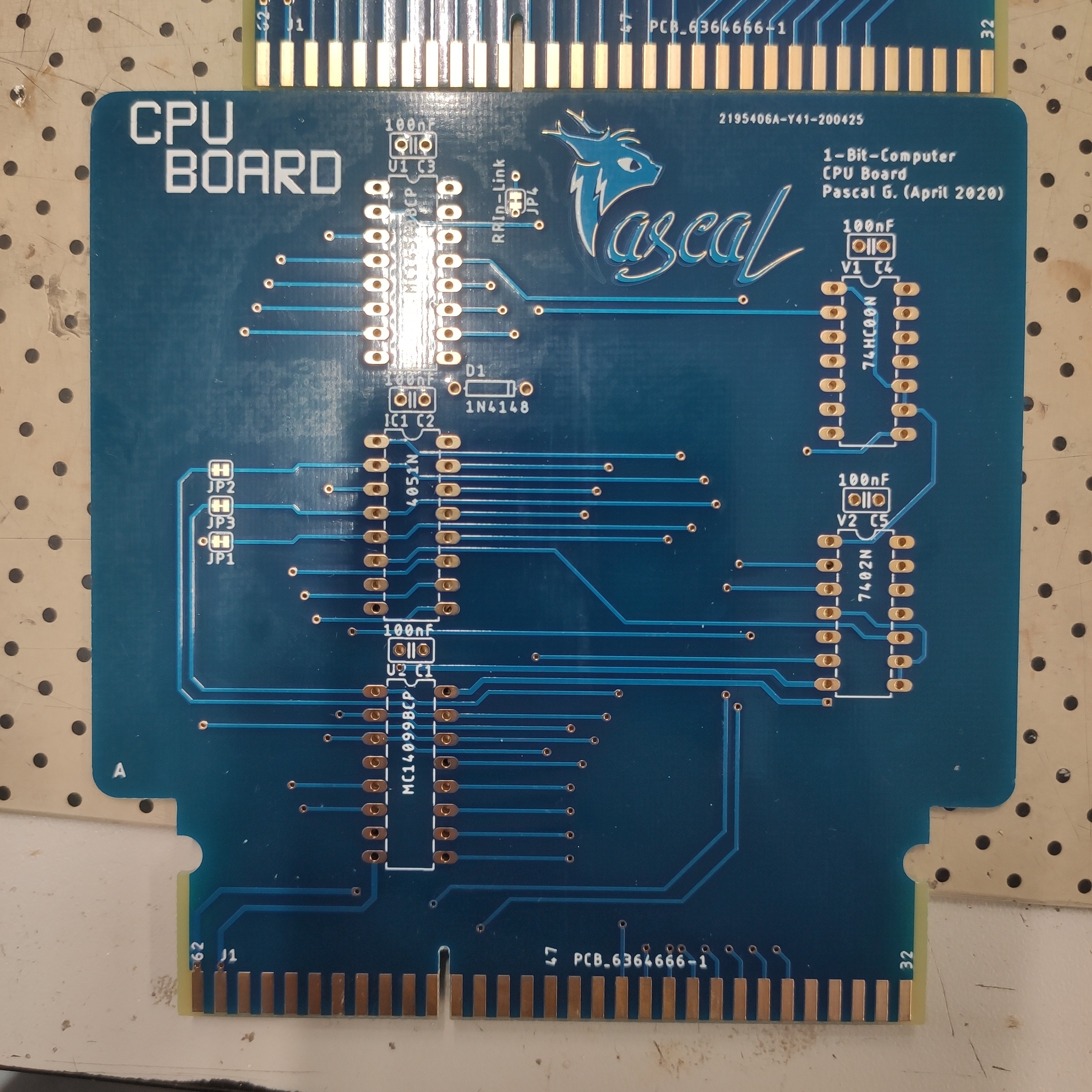
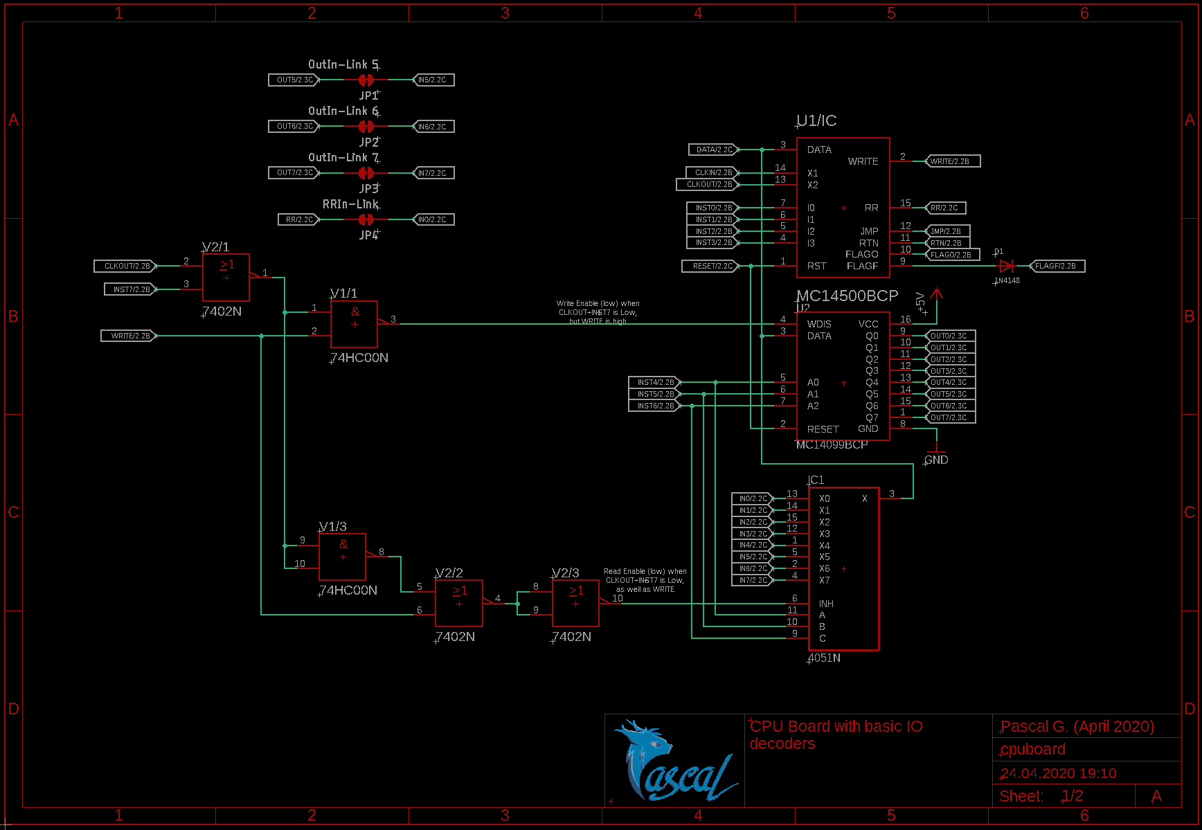
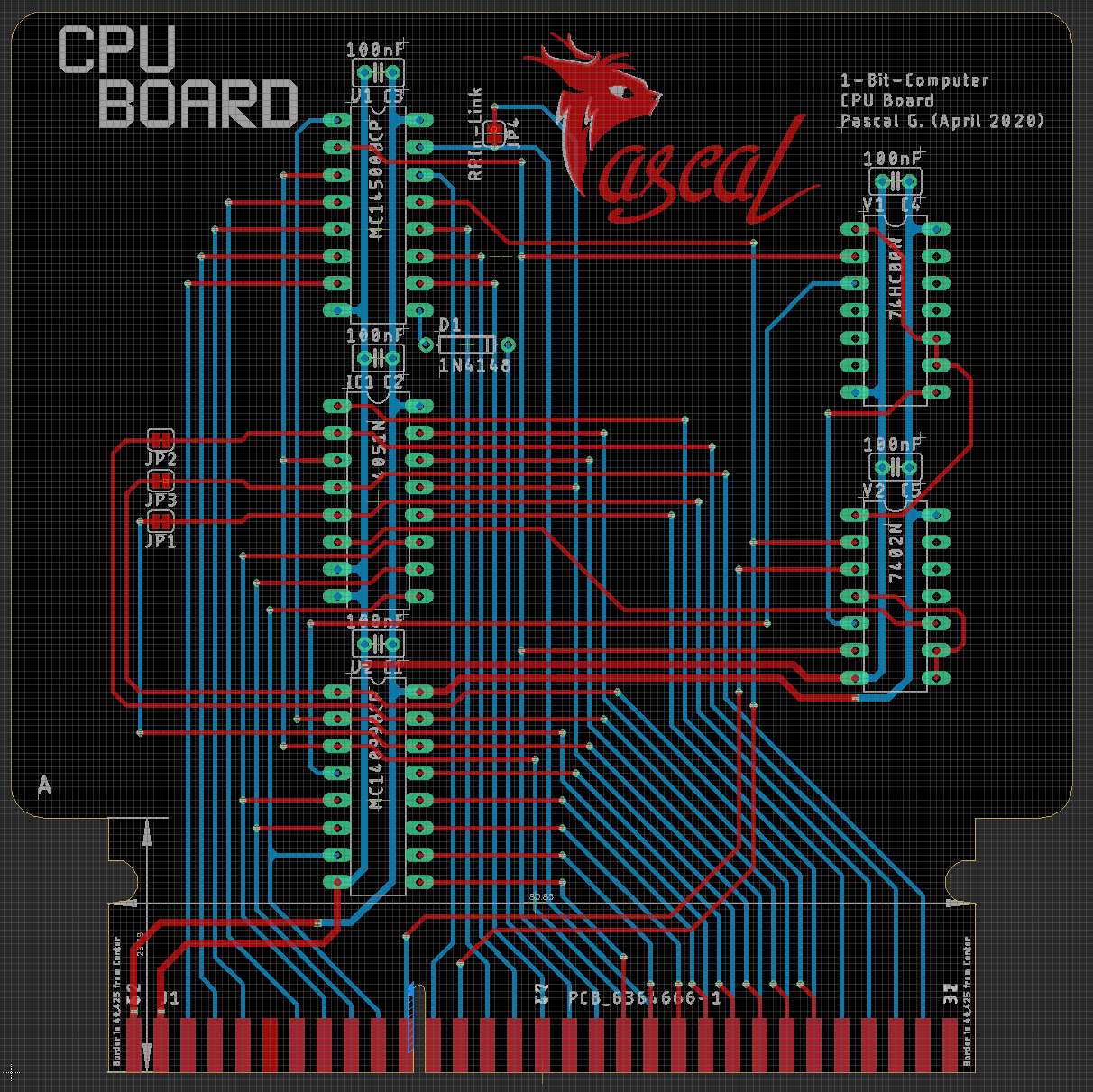
CPU Board
04/24/2020 at 19:01 • 0 commentsLast but not least, the CPU Board that holds the MC14500 ICU, together with a 8-Bit Input and 8-Bit Output IC. Instead of the MC14599 Input / Output chip, I use the MC14099BCP instead - or it's still available equivalent, the CD4099B, that is still sold and available on DigiKey.
![]()
![]()
With all boards organized and planned, there is nothing to start the production of them and ordering the components.
-
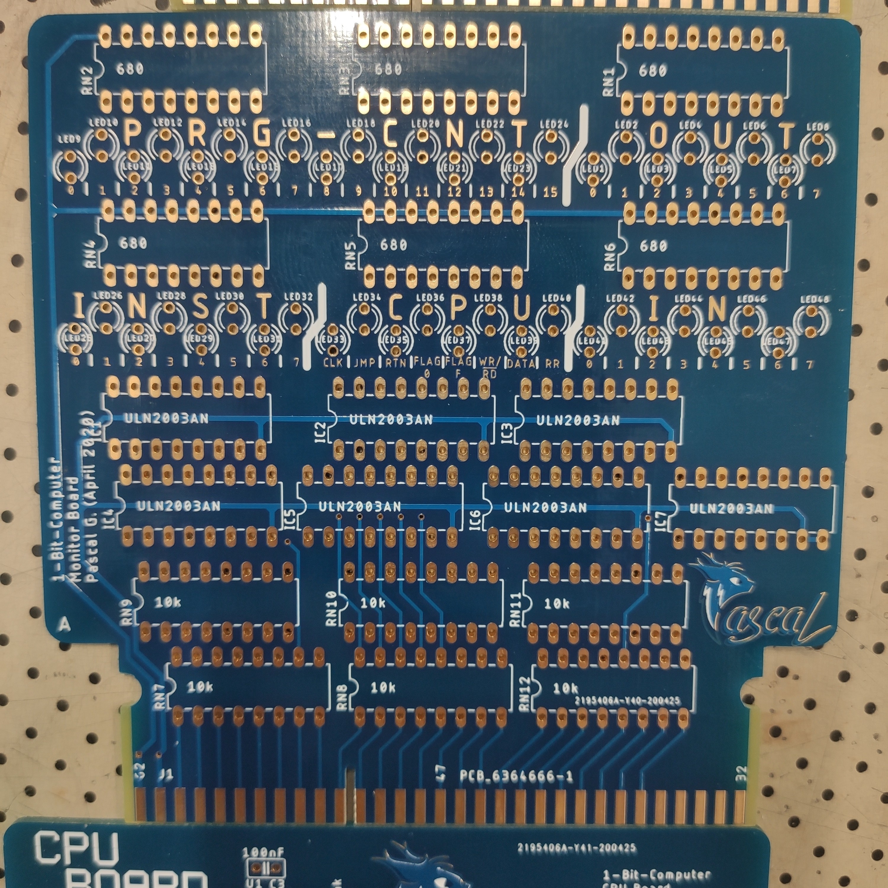
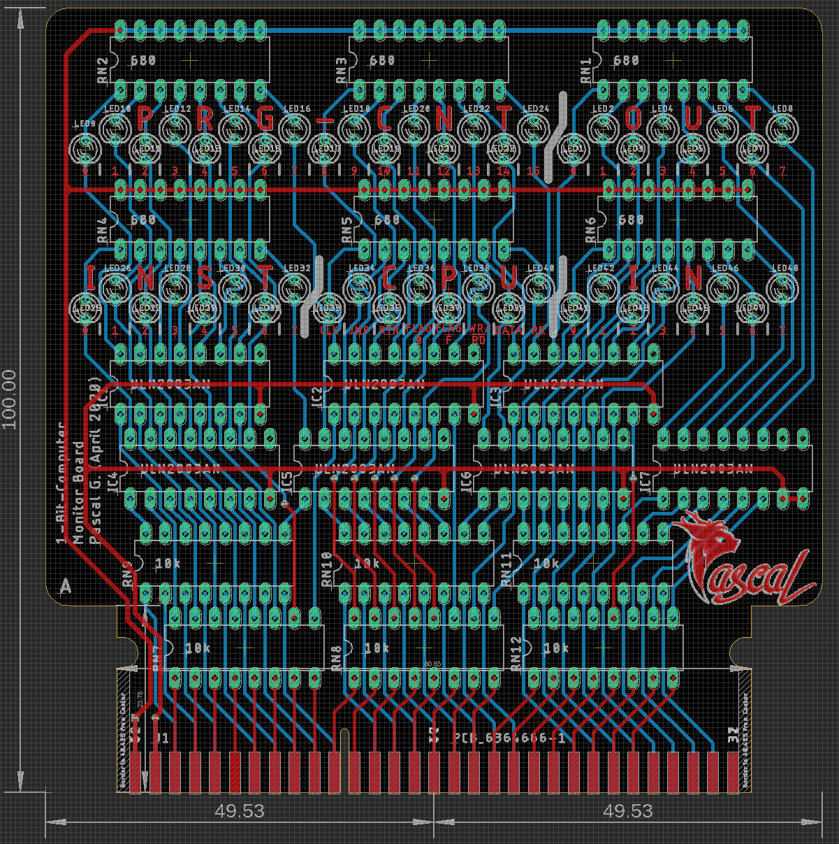
Monitor Board
04/24/2020 at 18:44 • 0 commentsA classic computer build isn't fully classic to me, until there is a panel full with blinkenlights!
So of course, this is a goal for me as well. As LED Driver I just went with the same ones that were used on the original WDR computer, the ULN2003.
To my surprise, fitting two A4 schematic pages worth of LEDs, Drivers and Resistors onto a 100x100mm board (which 28mm is taken up by the Card-Edge Connector) was not that easily - but that didn't stop me of course.
![]()
Had to get a bit creative with the way the LEDs are arranged, but I think it works out just fine like that. Basic Letters and Numbers in the top copper layer provide the basic info to quickly see which LED represents which signal from the BUS.
-
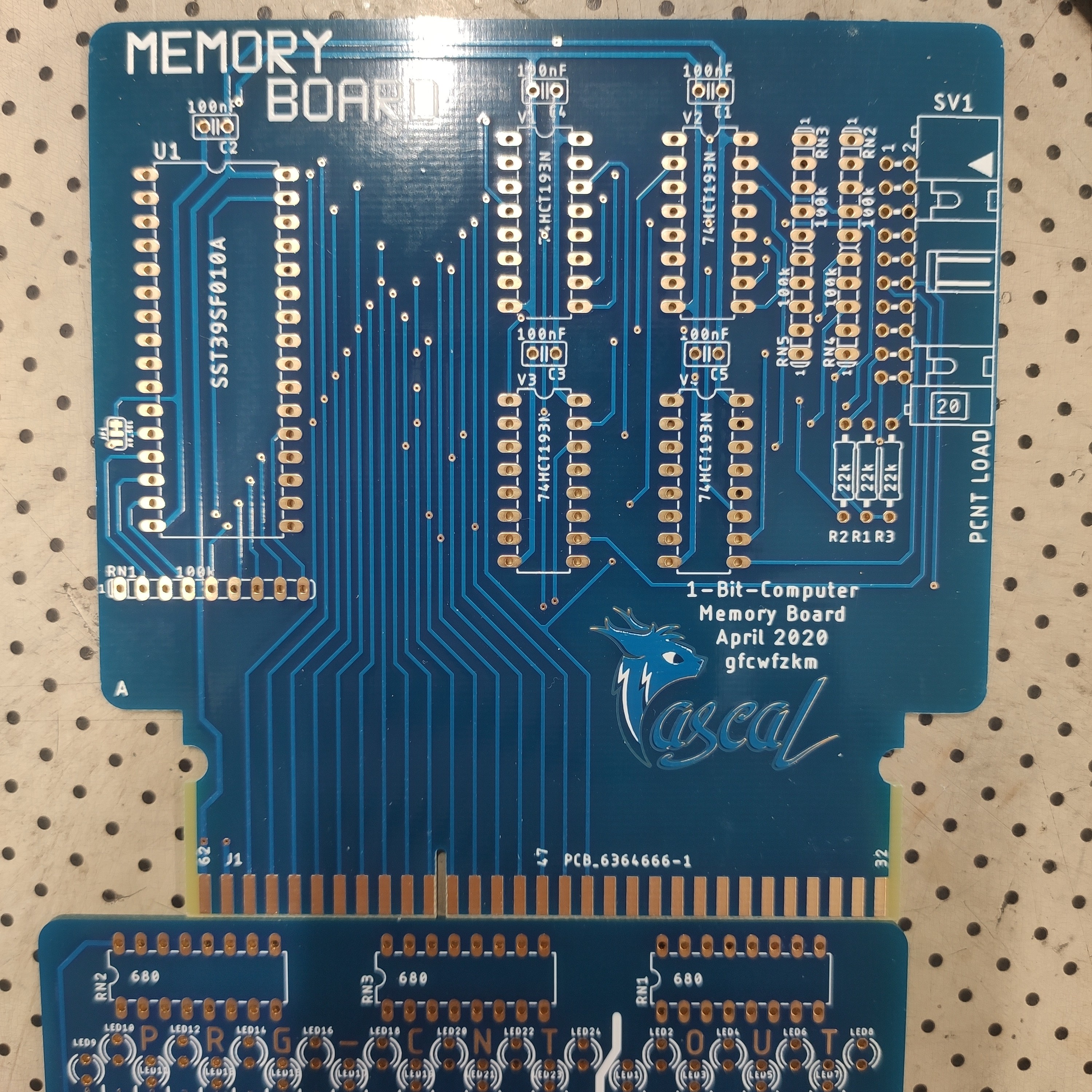
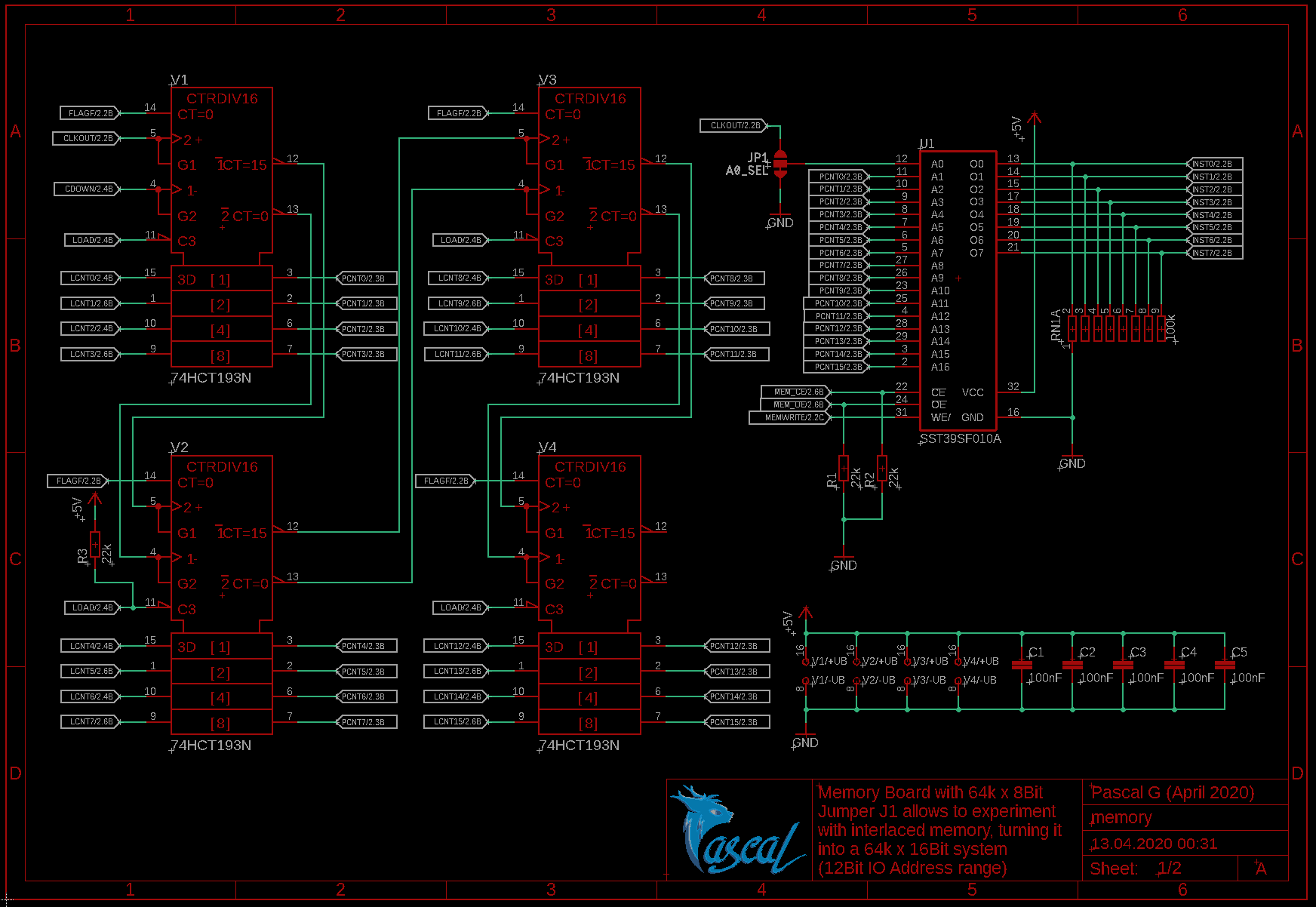
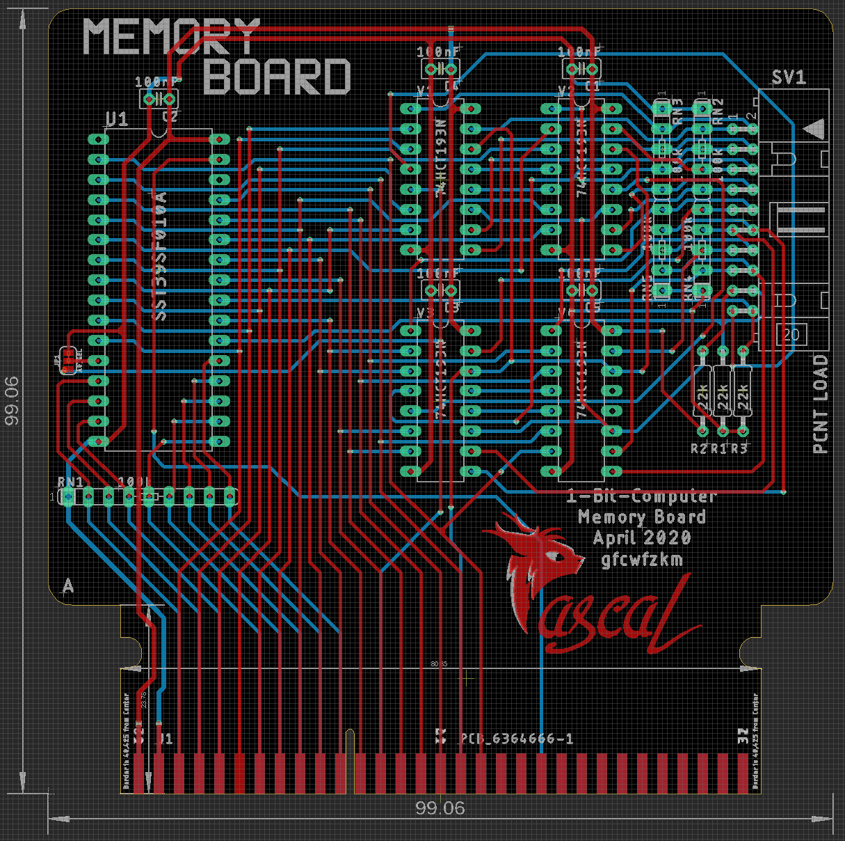
Memory Card
04/24/2020 at 18:22 • 0 commentsWith the mainboard taken care of, and a proper bus pinout defined, I decided to tackle the memory as next target. Compared to the original, I don't plan to use the old-style Intel 2112 RAM chips, but instead went for the cheapest non-volatile storage I could find on DigiKey:
The SST39SF010A![]()
With it's 128k Bytes of flash memory, it's a beast compared to the original 256 Bytes of RAM. Not sure what I will do with so much RAM, but since it's also one of the cheapest solutions with 1.13CHF, I decided to stick with it.
To handle the 17 Address Lines, I use four 4-Bit Counters (74HCT193) which leaves only one address pin left - A0.
A0 is hooked to a jumper, which by default is connected to ground, so the Computer behaves just like the original WDR one. Alternatively and with bit of solder and a knife, it can be connected to the clock signal instead. This allows to turn it inot a interlaced memory board, which brings a 12bit wide IO structure, compared to the default 4bit one. More about it can be found in Motorola's handbook about the MC14500.
A layout goal for the Computer Cards, are to stay within 100 x 100 mm of size. Here's the resulting layout:![]()
The connector on the right is hooked right up to the Address Counters, allowing to load a new address and to make it easier to implement a future, possible "jump & return" function.
-
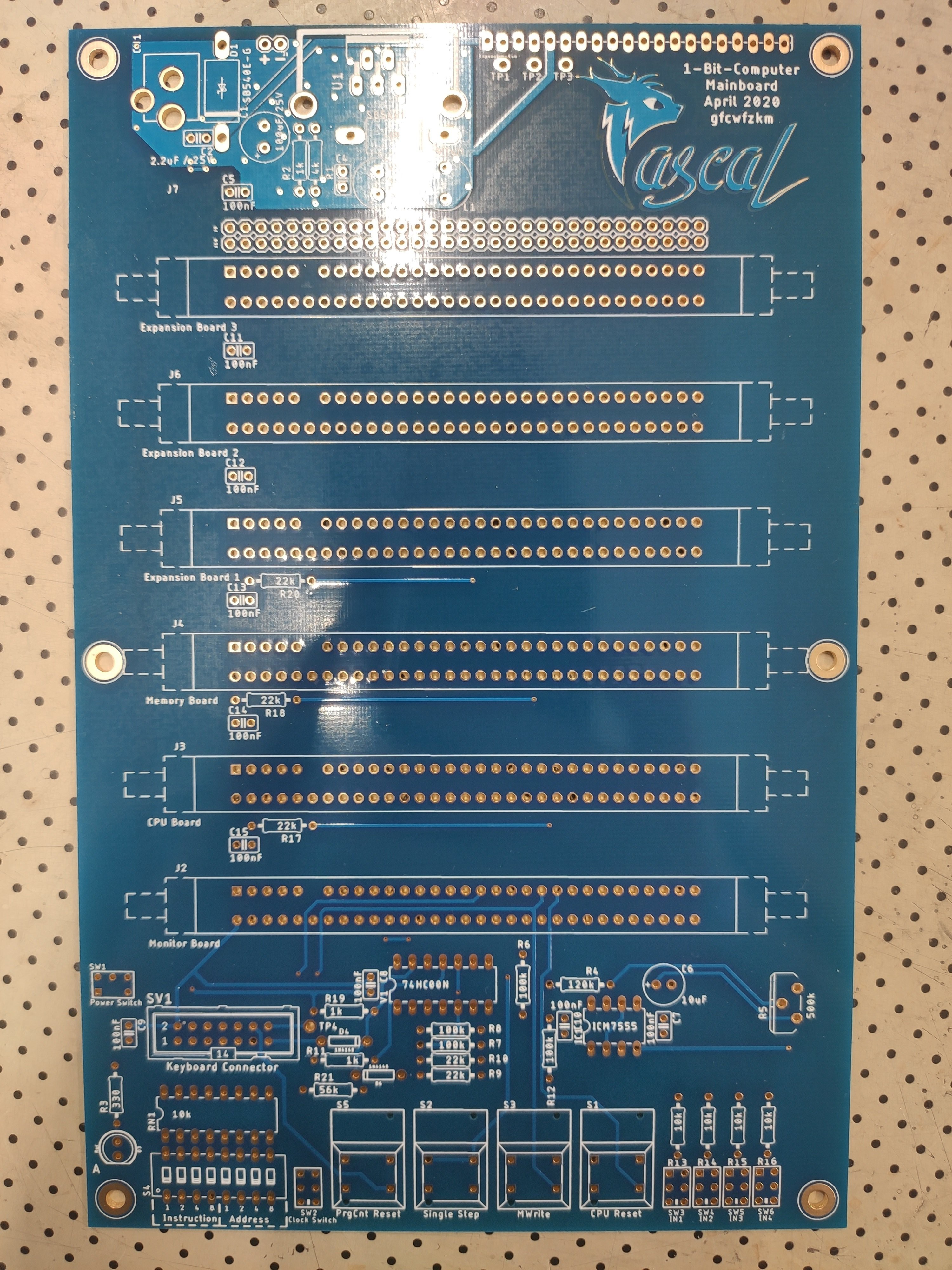
BUS System & Mainboard
04/11/2020 at 18:08 • 0 commentsAfter taking a closer look at the "BUS System" that the original 1-Bit-Computers used, I decided to make my own one which allowed for more flexbility. For that, I plan to use the card edge connector 6364666-1 by TE.
The mainboard is finally also done. Instead of no BUS slot but an expansion header, I added 4 unused expansion cards and the classic expansion header for downward compability. Also added a proper connector to add a external keyboard. The schematics are uploaded as .PDF together with a parts list.
(Also, still figuring out how this online HaDIO Web Editor works)
![]()
![]()
This is the BUS definition:
Pin Row 1 Name Description Pin Row 2 Name Description 1 +5V Voltage Rail 62 +5V Voltage Rail 2 GND Voltage Rail 61 GND Voltage Rail 3 INST0 Instructions (IO Address) 60 PCNT0 Program Address / Counter 4 INST1 Instructions (IO Address) 59 PCNT1 Program Address / Counter 5 INST2 Instructions (IO Address) 58 PCNT2 Program Address / Counter 6 - Omitted Pin & Hole 57 PCNT3 Program Address / Counter 7 INST3 Instructions (IO Address) 56 PCNT4 Program Address / Counter 8 INST4 Instructions (Actual Instruction) 55 PCNT5 Program Address / Counter 9 INST5 Instructions (Actual Instruction) 54 PCNT6 Program Address / Counter 10 INST6 Instructions (Actual Instruction) 53 PCNT7 Program Address / Counter 11 INST7 Instructions (Actual Instruction) 52 PCNT8 Program Address / Counter 12 CLK IN MC14500 Clock IN
(Used to define the clock)51 PCNT9 Program Address / Counter 13 CLK OUT MC14500 Clock Out
(Used for Peripherals)50 PCNT10 Program Address / Counter 14 JMP Jump Signal (Not used) 49 PCNT11 Program Address / Counter 15 RTN Return Signal (Not used) 48 PCNT12 Program Address / Counter 16 FLAG 0 Flag 0 Signal (Not used) 47 PCNT13 Program Address / Counter 17 FLAG F Flag F Signal (Causes the
Program Counter to (Preset/) Reset46 PCNT14 Program Address / Counter 18 WR/!RD Write / Read IO 45 PCNT15 Program Address / Counter 19 DATA Data BUS 44 OUT0 Output 20 RR Result Register Output 43 OUT1 Output 21 MEMWRITE Write-Enable Signal for
the Program Memory42 OUT2 Output 22 RESET CPU Resets the CPU and
IO Peripherals41 OUT3 Output 23 IN0 Input (connected to
the Result Register)40 OUT4 Output 24 IN1 Input 39 OUT5 Output 25 IN2 Input 38 OUT6 Output 26 IN3 Input 37 OUT7 Output 27 IN4 Input 36 N.U. Not used, but routed on the Main Board 28 IN5 Input (connected to Out 5 on
CPU Board by a Jumper)35 N.U. Not used, but routed on the Main Board 29 IN6 Input (connected to Out 6 on
CPU Board by a Jumper)34 N.U. Not used, but routed on the Main Board 30 IN7 Input (connected to Out 7 on
CPU Board by a Jumper)33 N.U. Not used, but routed on the Main Board 31 N.U. Not used,
but routed on the Main Board32 N.U. Not used, but routed on the Main Board -
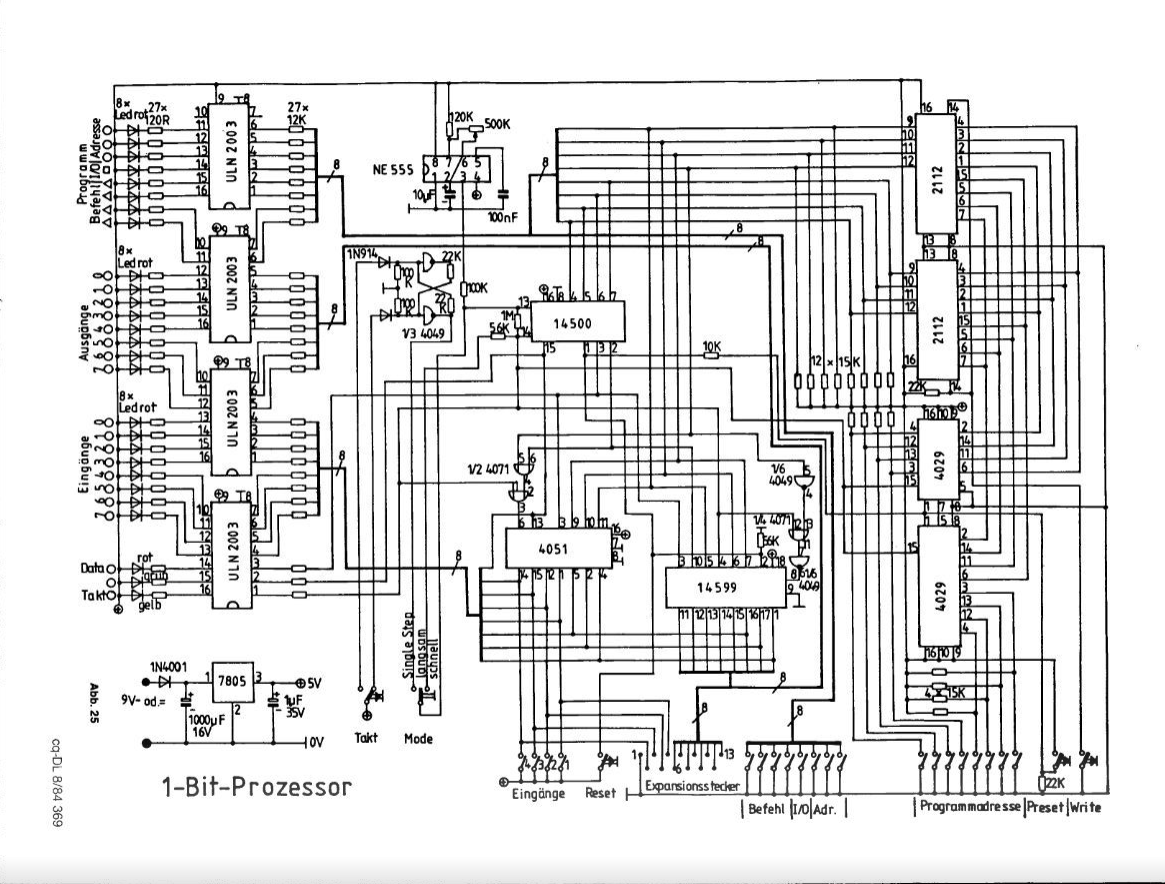
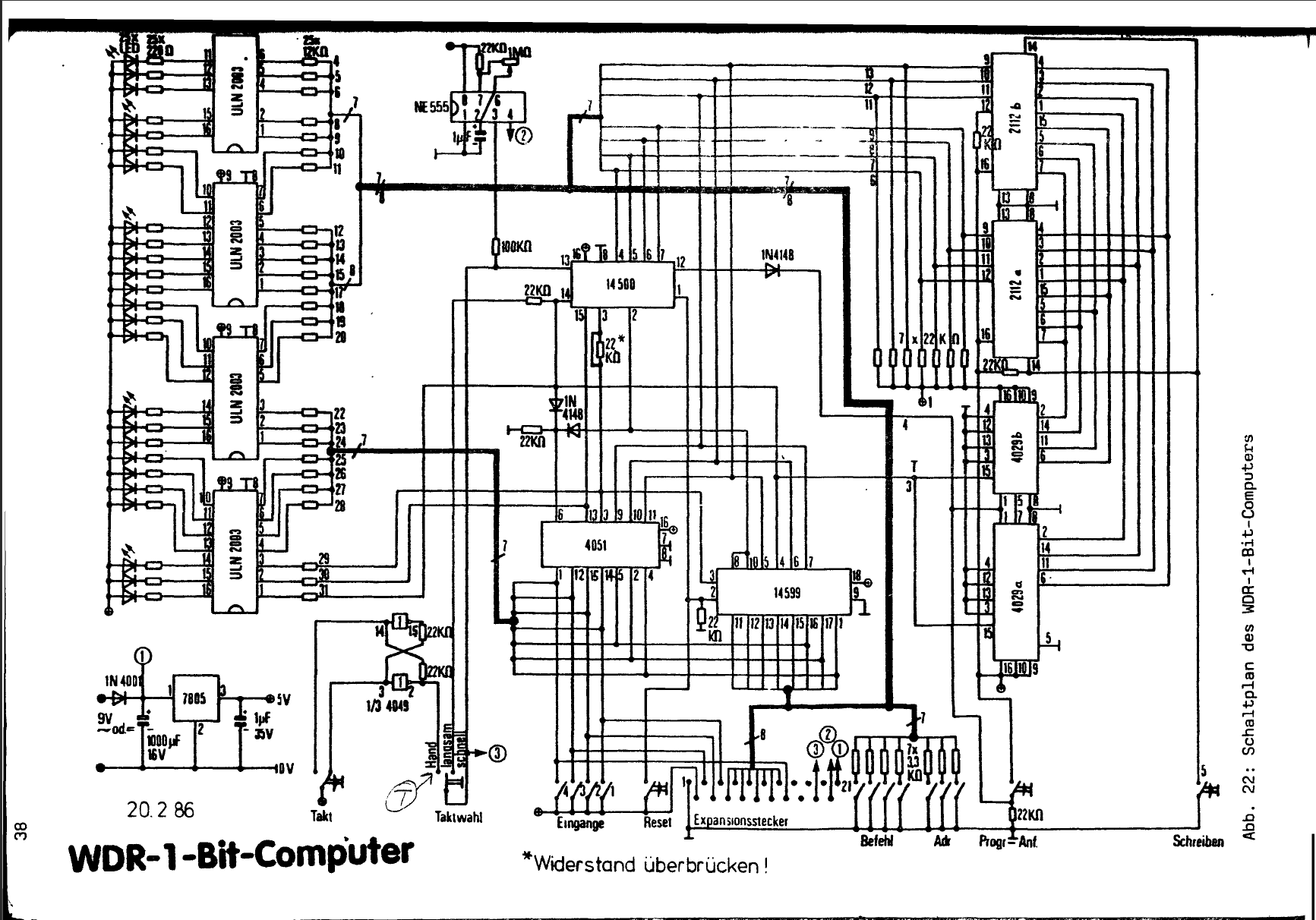
Collecting infos of the real computer
03/25/2020 at 11:32 • 0 commentsI've been looking for some documentation and data about both the computer and some of the special parts for a while now, and lucky there is a website that seems to provide a lot of scanned data and even pictures, with a second website showing a different-looking version of it.
1: http://wdr-1-bit-computer.talentraspel.de/
2: https://www.old-computers.com/museum/computer.asp?st=1&c=834 and
3: https://www.old-computers.com/museum/photos.asp?t=1&c=834&st=1The training computer on the pictures from the old-computers website shows quite a some differences compared to the scanned documents and pictures on the wdr-1-bit-computer website. I assume that one computer was built according to the WDR instructions, while the other might have been built like it is printed on the cqDL Magazine.
![]()
![]()
It seems like the cqDL (lower schematic picture) version seems to have some additional features compared to the more lightweight WDR version, but it also looks like that both versions are software compatible to eachother. The idea of manually setable program address and to have another I/O-select-Address compared to the WDR version definitely will be integrated into my version, if not further expanded.
Both magazines provide excellent documentation and will be used as references. The WDR Magazine seems to be more a guide, teaching the very basics as well, but also shows many possible expansion modules and their features, while the cqDL Magazine prints it more compact.
Now the next step for me is to see which components are still available, where I can get them and which components I can replace with newer ones. I can imagine the biggest issue will be the 1-bit CPU MC14500 itself, but luckly I got 5 of them from ebay. But if I ever decide to turn this into a full kit, I gotta think of an alternative.