Samuel A. Falvo II
-
BX-Plorer: Meet the New Card, Same as the Old Card
10/08/2020 at 20:11 • 0 commentsAs this project evolves, I'm noticing a distinct yet synergistic compartmentalization in the roles and responsibilities of different project components. When I started this VDC-II project, I'd just been convinced by interested members of the community of the value of developing Kestrel-3 computer parts for the RC2014 backplane. I later observed that my RC2014 Zed's flash BIOS image could be built with Commodore VDC support, and after reading up on that chip's technical specs, I realized that it was a fairly close match to what I'd wanted to achieve with my own CGIA concept. So, rather than re-inventing the video support with the CGIA, I figured I'd just piggy-back what was already there, and decided to reimplement the VDC. This benefits both RC2014 and Kestrel-3 communities, since any Kestrel-specific enhancements I make to the design later on can benefit both communities, not just the one. So, I set out to just develop a (mostly but not completely compatible) clone of the Commodore 8563 VDC as used in the Commodore 128, using affordably priced, off the shelf FPGA development boards. That became the VDC-II project you're reading about now.
I've always intended to release this project as a kit of some kind, so that RC2014 owners can, in long-standing RC2014 community tradition, build their own video card. That means, as part of the kit, they'd receive the PCB, all the chips, a pre-programmed TinyFPGA BX module, and other miscellaneous parts needed to have a working video card.
However, I now realize that the very circuit I used to interface my TinyFPGA BX module to the RC2014 backplane is itself useful as a self-standing product in its own right. You could see a less developed realization of this, more or less explicitly, in previous log entries where I first mention breaking up the FPGA part of the circuit from a mezzanine card containing the analog VGA circuit.
Going forward, I've decided to formalize the separation of the FPGA project card from its applications. First, the FPGA project card now has an official name: BX-Plorer. It lets the consumer of the card explore FPGA designs using the TinyFPGA BX module.
Second, I've decided to factor the BX-Plorer out into a separate git repository. I'll update my Hackaday.io configuration accordingly shortly after making this post. This implies that, Coming Soon, there'll be a separate Git repository for the VDC-II design files and the software stack needed to drive it. I'll (re)post updated links in a separate log when everything is in place.
Related to the first two points above, for now, both BX-Plorer and VDC-II updates will happen in this Hackaday.io project. As I write this, I have no plans of factoring the two projects out here. These two projects have been co-developed from the get-go, and I don't see that changing any time soon.
Third, what of the VDC-II-based RC2014 "video card"? Is that now dead? As I'd originally conceived it, yes. With all the other video card projects that people are concurrently producing for the RC2014 (link 1, link 2, link 3), it's not clear to me how I can compete for mindshare. However, if there's enough feedback, I can see offering a BX-Plorer Cost Reduced/Fixed Function card as a dedicated video card. If this is something that is still desirable to readers, please do get in touch to let me know.
(Besides, you can always use a regular BX-Plorer with a pre-programmed TinyFPGA BX and analog VGA mezzanine still.)
Fourth, this does not affect the development of the VDC-II itself. I still need a video card, for both my RC2014 and for my own future homebrew computer design. The VDC-II project is not dead.
When, not if, you see these new terms being bandied about in my project updates, now you'll know why and where they come from. :) Until next time!
-
Revision 5 Circuit Design Underway
10/08/2020 at 18:05 • 0 commentsAs I continue to read up on my responsibilities for working with Crowd Supply (CS), I realize that, being a vetted interaction process, CS is almost certainly going to call me out for not exposing all of TinyFPGA BX's I/Os. So, I'm going to head that issue off now and work to expose all of the I/Os that this module has to offer. This will in effect turn the card into a generic FPGA development card. I'll mention more about this in a related but separate project log update.
This is not as simple of a task as it sounds; I need to:
- create a new TinyFPGA BX schematic symbol.
- create a new TinyFPGA BX footprint for PCB layout.
- figure out how to expose all the I/Os.
- create revised schematics and PCB layout.
These steps took me about three days so far, and I'm still working to complete the list. Here's a summary of the changes I've made to the design so far and what can be expected from revision 5A boards.
First, the dedicated 2x7 pin socket that I'd intended to replace the 14-pin DIP socket (in an unreleased revision 4B PCB design; you can see it in the Github repo though) has been replaced by a set of three 2x6 pin sockets, spaced 0.9" apart, and whose pinouts comply with Digilent's Pmod interface specifications at 3.3V. I'm currently placing them across the top of the PCB for easy access, as that's the only edge long enough to accommodate them. This brings 24 I/Os out for general purpose use. There's a catch, though; these sockets are not right-angle sockets. I intend these sockets to be used with Digilent's 12-conductor Pmod cables to attach devices to. The PCB is already big enough to flop around in the RC2014's single row backplane socket, so you don't want to put too big of a load on those sockets. Building a mezzanine card will extend the height of the PCB, which will make it more floppy and less mechanically sound than it already is. Cables can be routed, which enables them to also act as strain reliefs. That said, if I can source through-hole, right-angle connectors, they should be drop-in compatible, if you can find a way to mechanically secure the contraption.
Second, I will bring out the 5 shared I/O pins to a 2x3 pin *header*. This header will have a comparable pin-out to the TinyFPGA BX pin cluster. Being that these will be exposed pins, you can connect to them using Dupont connectors.
Between these two changes, the BX's remaining 29 I/O pins will be fully and much more easily accessible to hardware hackers.
-
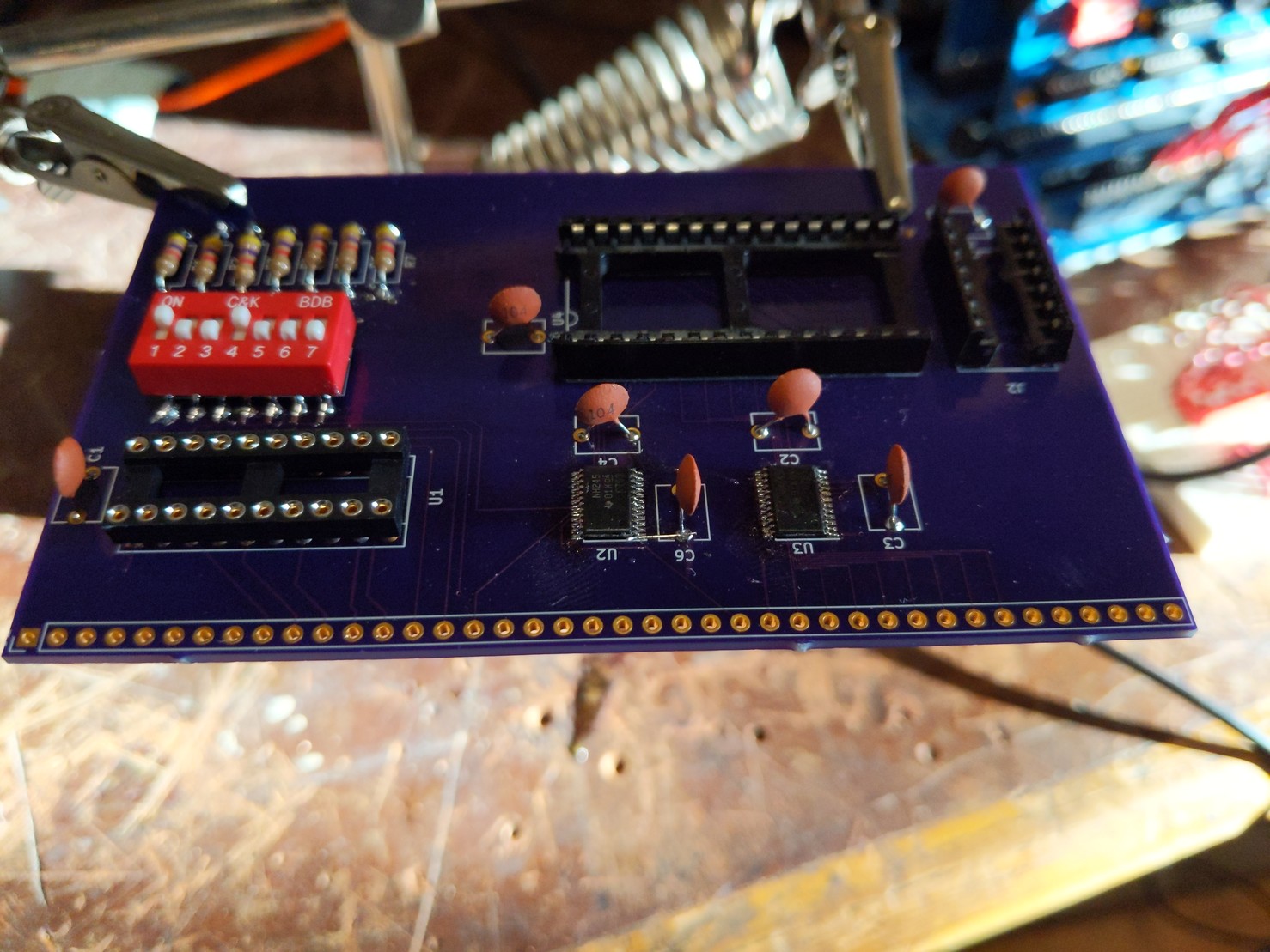
Revision 4A PCB Built, Works
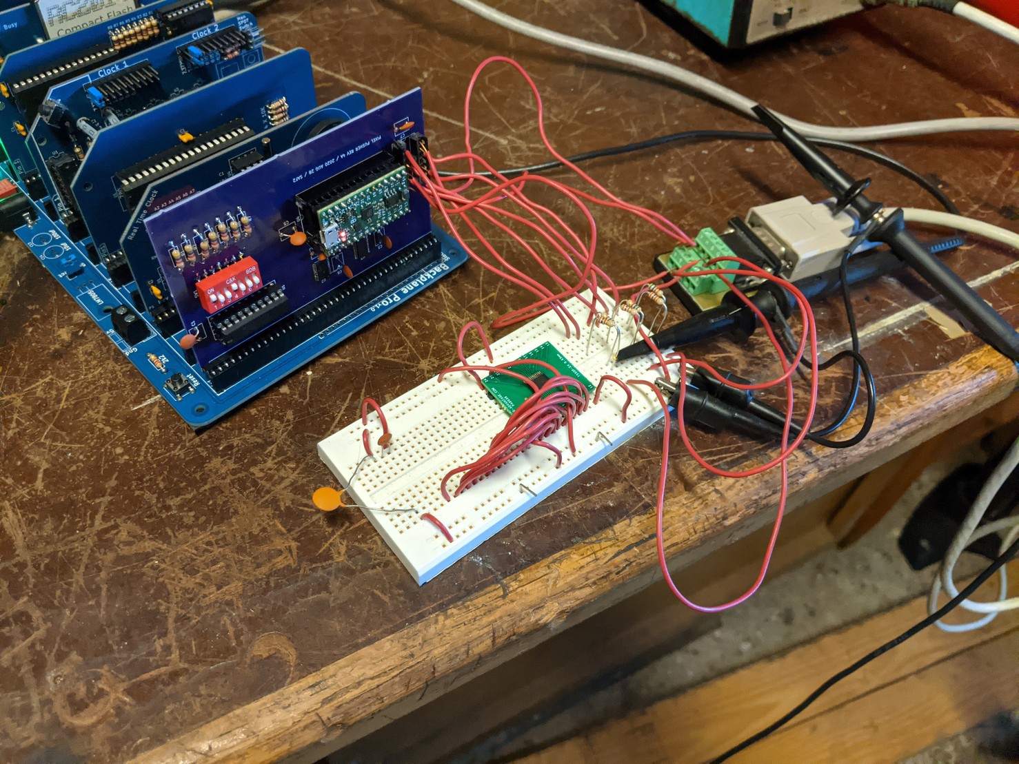
09/24/2020 at 22:23 • 0 commentsJust wanted to say that I finally completed building the revision 4A board; most of the hardware was discussed in the previous log entry, but I've fitted the '688 comparator for address decoding as well as the TinyFPGA BX module. The result is shown in the pictures below.
I'm happy that, despite needing one bodge wire from U2 to +3.3V, it is otherwise fully capable of working from the POV of software development.
I've already made the changes to the design files to support revision 4B, which fixes all the known hardware bugs. Additionally, the nMigen files for the VDC-II has been configured to output 9-bit video, so all 11 output I/Os are known to work.
Besides getting revision 4B out the door, all that remains is a set of mezzanine boards: one for VGA, and one for PS/2 keyboard and mouse. That, combined with a reasonable GEOS-like GUI system, should be sufficient to make the RC2014 into a reasonably usable homebrew computer system.
![]()
![]()
-
PCBs Received, First Build
09/18/2020 at 17:25 • 0 commentsOn the 14th, I received my printed circuit boards for the Pixel Pusher. Yesterday, I got around to trying to build one of the three prototype boards I received.
![]()
This is what a bare board looks like, component side up.
![]()
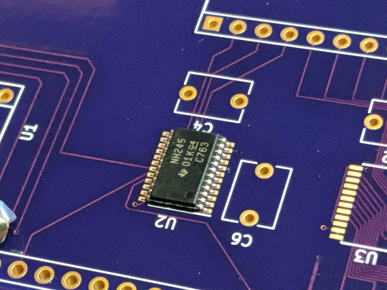
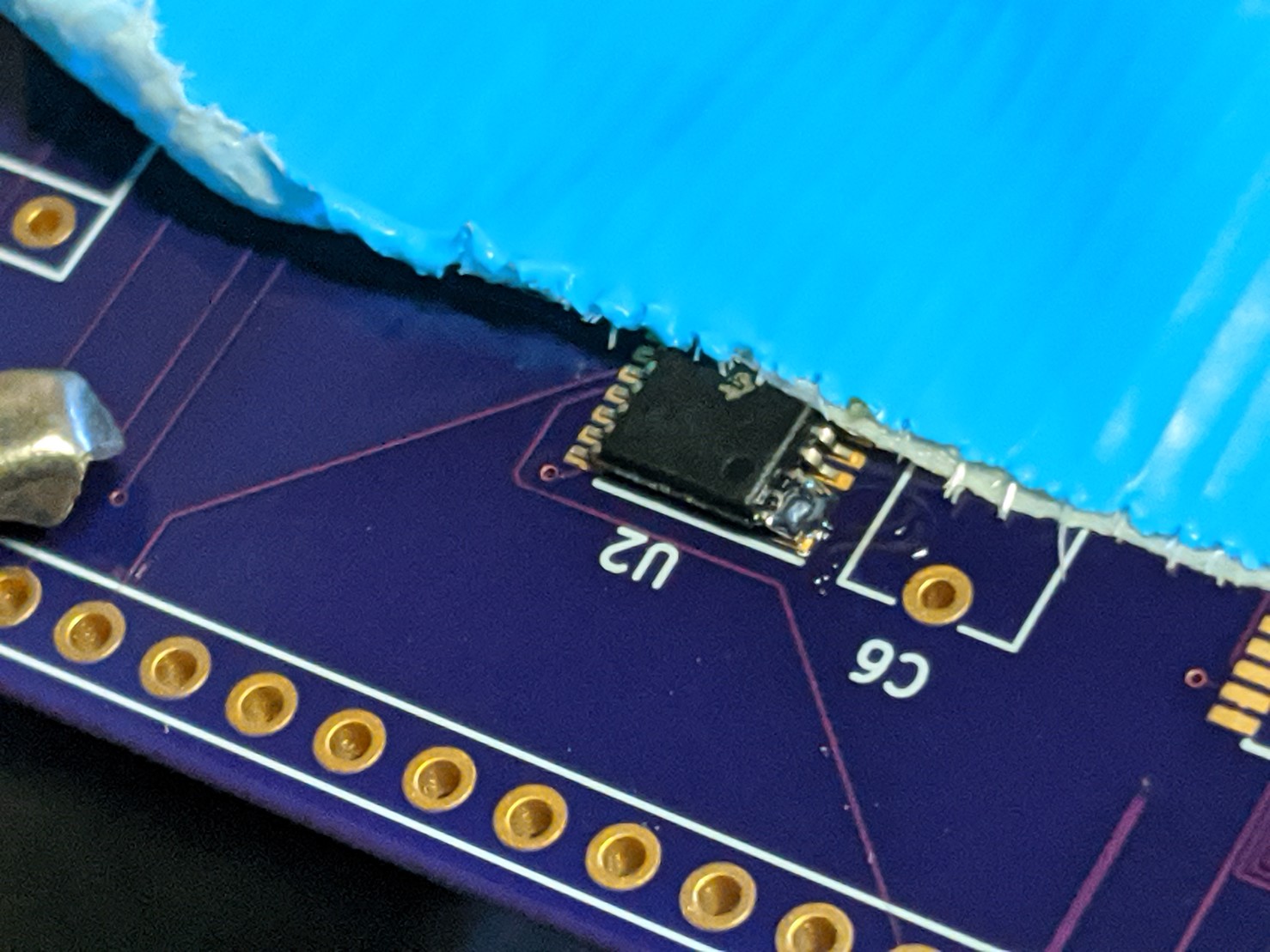
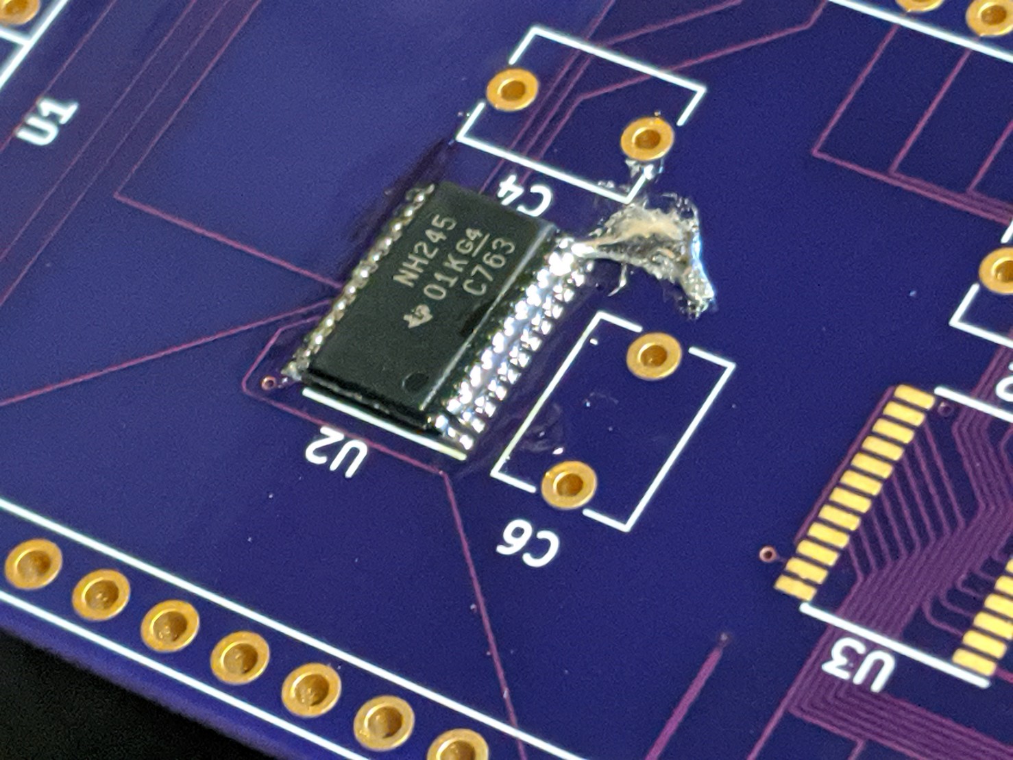
My first task is to place the highest risk components first, so as to just get them out of the way. In this case, the two 74LV8C245PWR chips, as they're incredibly small devices that even an idle breeze can cause to slip off and never be found again.
![]()
I use blue duct tape for this purpose which is not the best thing to use but it's all I had available. Tacking one corner of the chip down is sufficient to hold it in place.
PRO TIP: The ideal tape for this would have been blue painter's tape. In order to reduce the stickiness of the duct tape down to something comparable to painter's tape, I just applied and removed the duct tape strip off the work bench several times until I was comfortable with the strength of the remaining glue. The workbench was naturally dusty, so each application added more dust to the strip, which had the effect of reducing how sticky the strip was.
![]()
I next applied liberal amounts of solder to the chip's connections. This ensured all pins were soldered to the pads, but it also ensured that all pins were soldered to each other as well. This excess solder had to be removed. I used solder wick for this purpose.
![]()
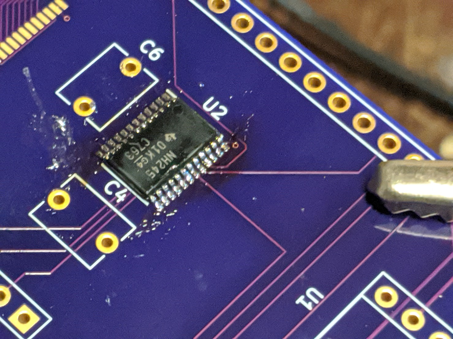
After fighting a bit with the solder wick (as evidenced by the slightly scorched flux residue), I sopped up all of the excess solder. Solder wick does not remove everything, and it happens to work out that what remains is sufficient to both hold the chip in place and to ensure good contact.
Because the contacts are so small, however, It is best to perform continuity checks with other parts of the circuit. If you need to desolder and resolder/reflow the contacts on these parts, now is the time to do it before other components are added.
I just discovered that the 3.3V supply pin of U2 is not connected to the 3.3V trace. I forgot to place a via! I'll need to add a bodge wire later.
![]()
After repeating the steps above for the second level shifter chip, I'm left with a board with two nicely soldered, surface-mount chips. Thankfully, I didn't discover any more missing connections!
![]()
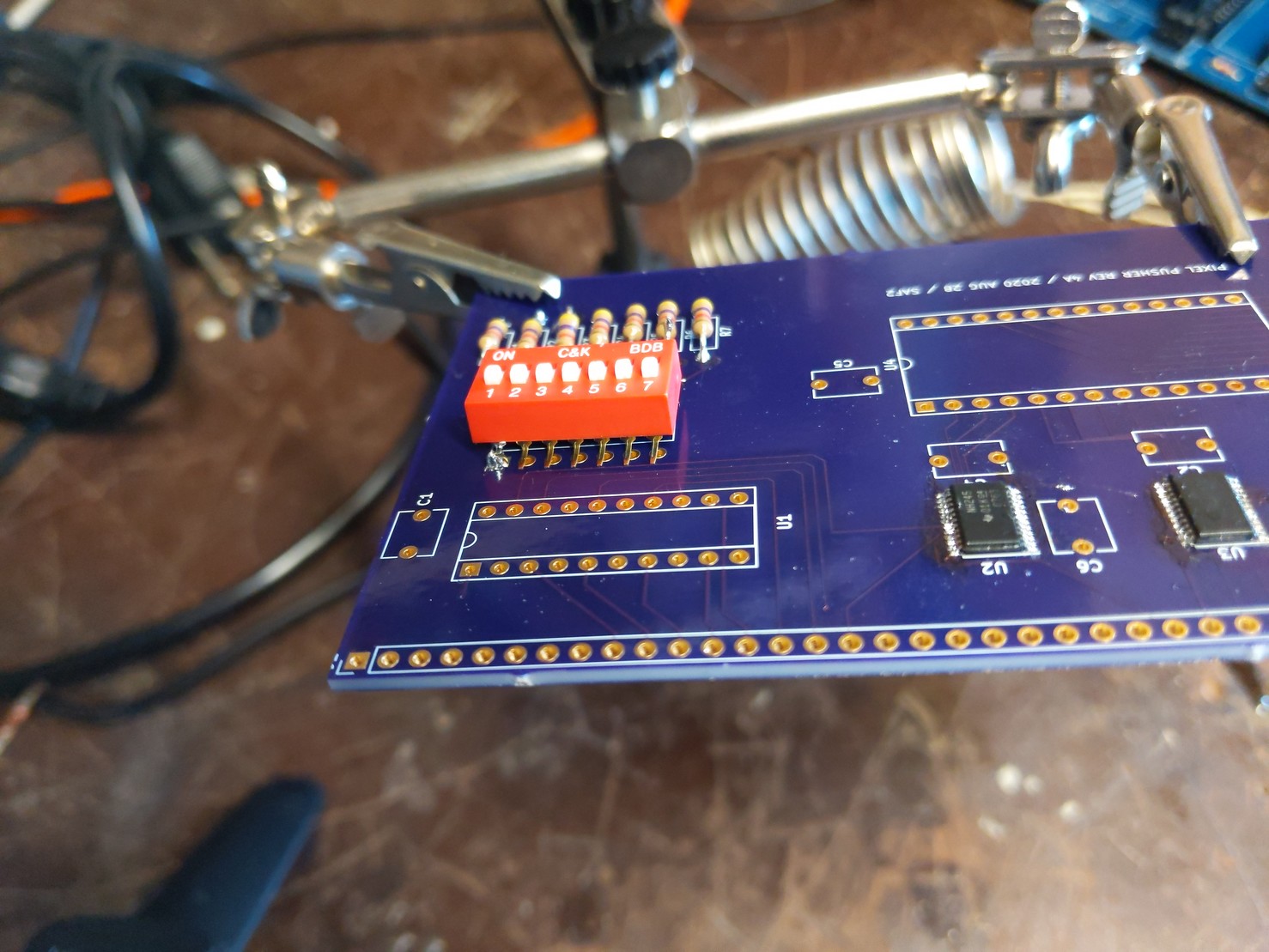
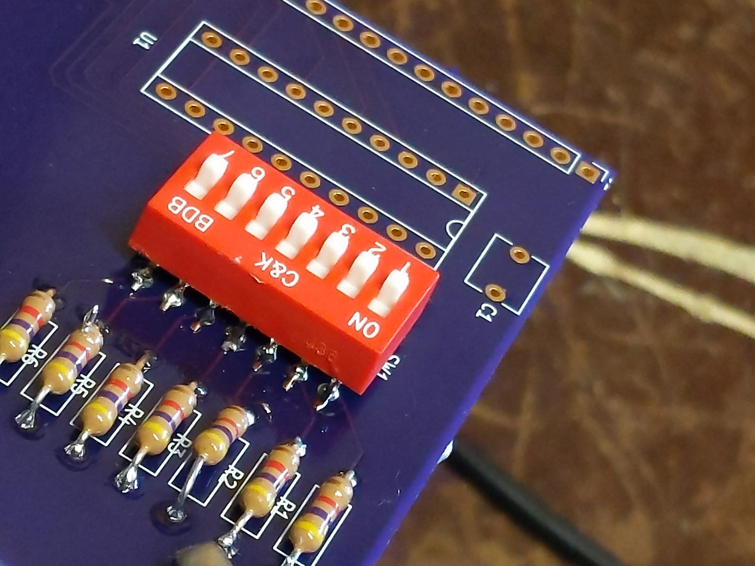
I found out the hard way that the footprint used for the DIP switches (which should have been a normal 14-pin DIP footprint) was too wide for the actual switch. Thankfully, I could splay the legs of the switch out and make surface contact with all the holes on the component-side of the board. Since all the holes are fully plated through (per OSH Park's website and as continuity checks confirm), treating the DIP switch package as a surface mount device instead of a through-hole device provides the extra length needed to ensure good contact with the rest of the circuit.
So, I splayed the pins out, tacked opposite corners of the DIP switch down, and ...
![]()
proceeded to blob solder on the remaining pins. I then set the DIP switches so that the card will respond to I/O ports 6Eh and 6Fh (not shown). I then set the DIP switches on the breadboard prototype to respond to I/O ports 6Ch and 6Dh, which would allow me to have both VDC-IIs in the RC2014 circuit at the same time without contention.
![]()
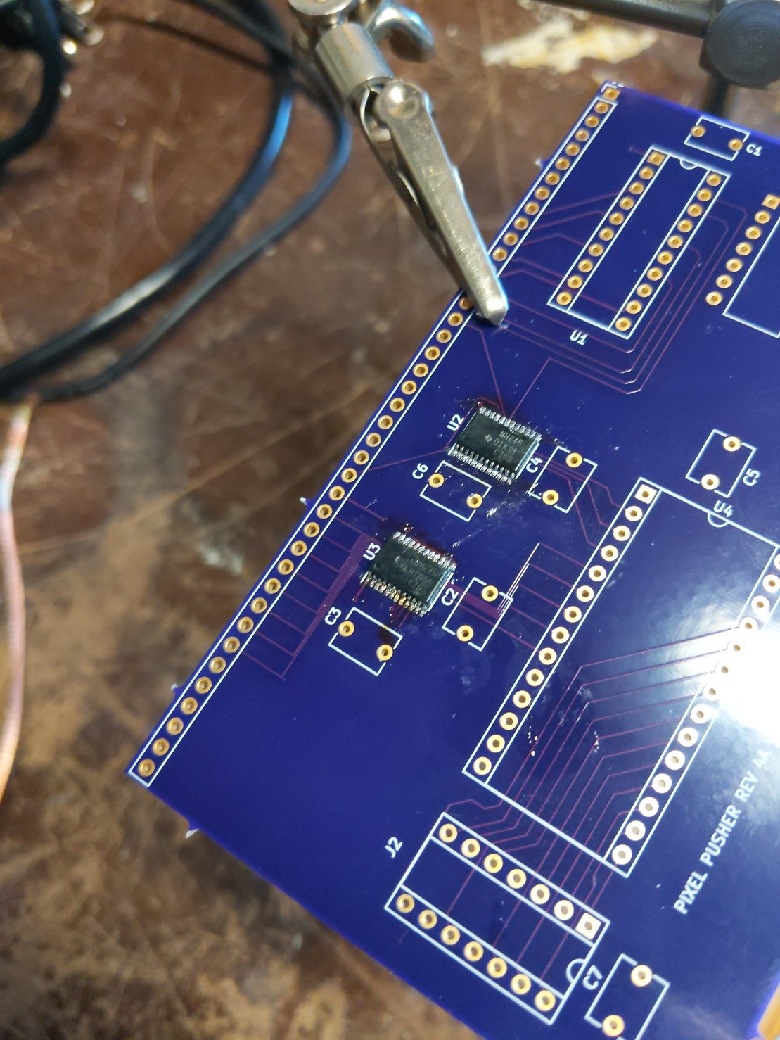
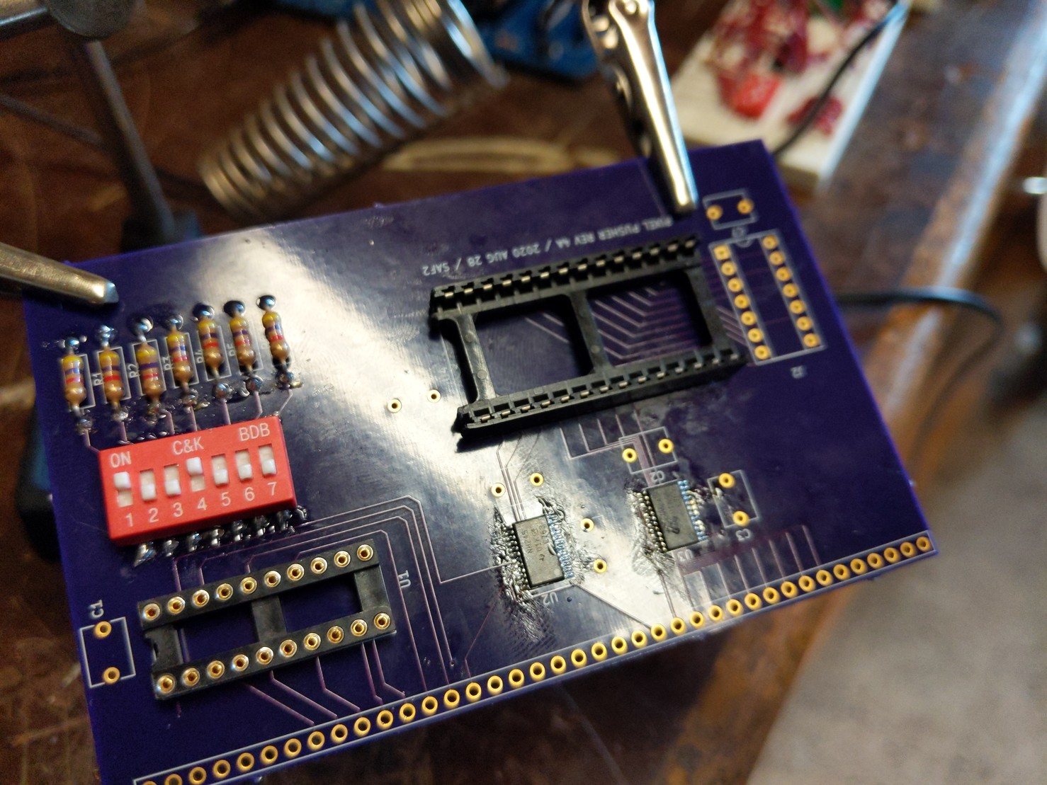
Next, I needed to fit a 28-pin, 0.6" wide socket for the TinyFPGA BX module. However, I didn't have any on-hand. Disturbing; I believe I ordered these some time ago via Amazon. Whatever, no biggie; I instead took a spare 40-pin socket I had available and chopped off six pins on either side. The result fits perfectly.
![]()
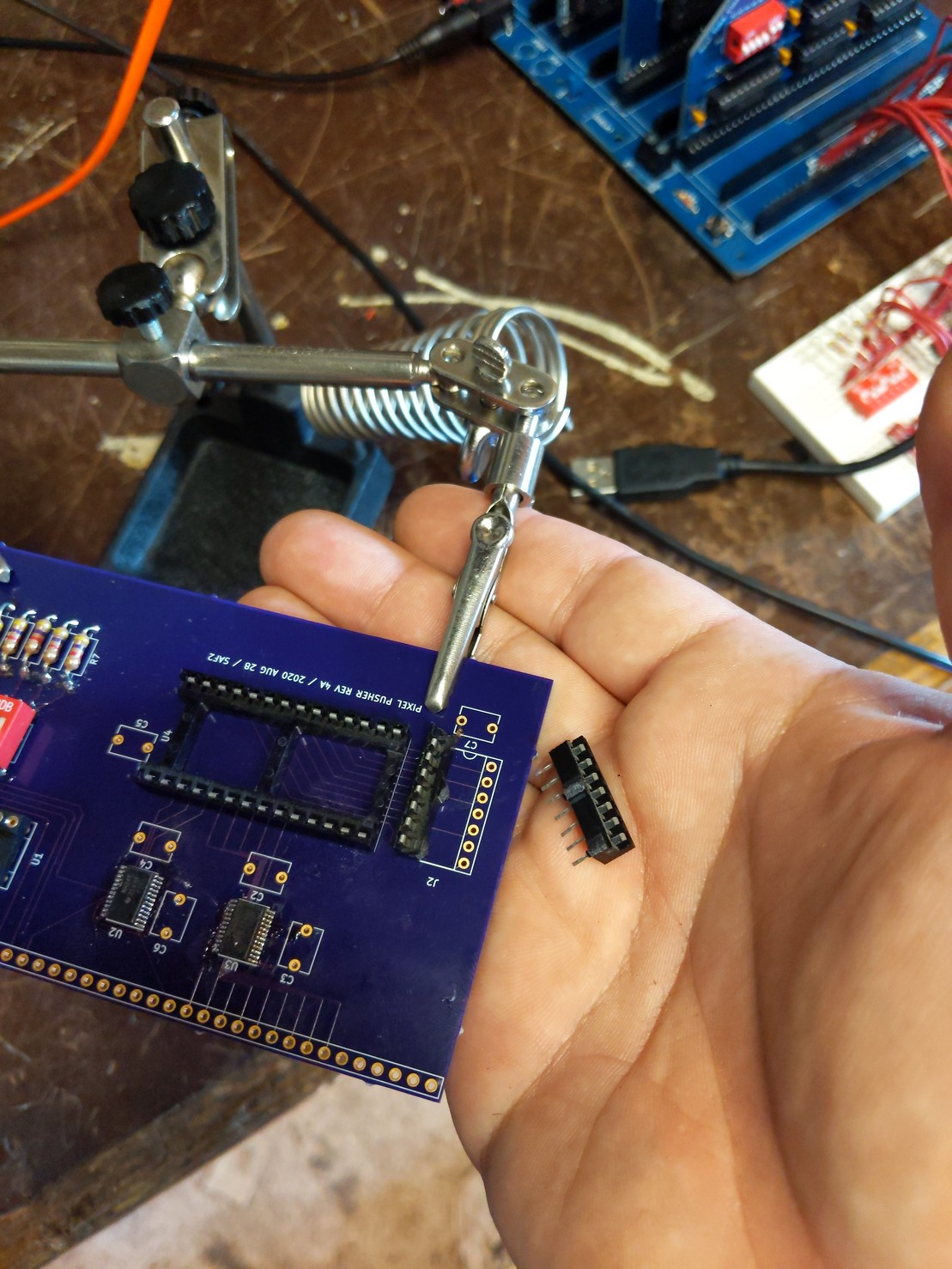
More hackery was required, as I also found out I didn't have any 14-pin DIP sockets handy either. So, I took another 0.6" wide socket (24-pin, in this case) and performed surgery on it to produce two make-shift 7-pin SIP sockets. I then placed them onto the PCB, and squeezed them together until they were 0.3" apart, roughly, which you can see below.
![]()
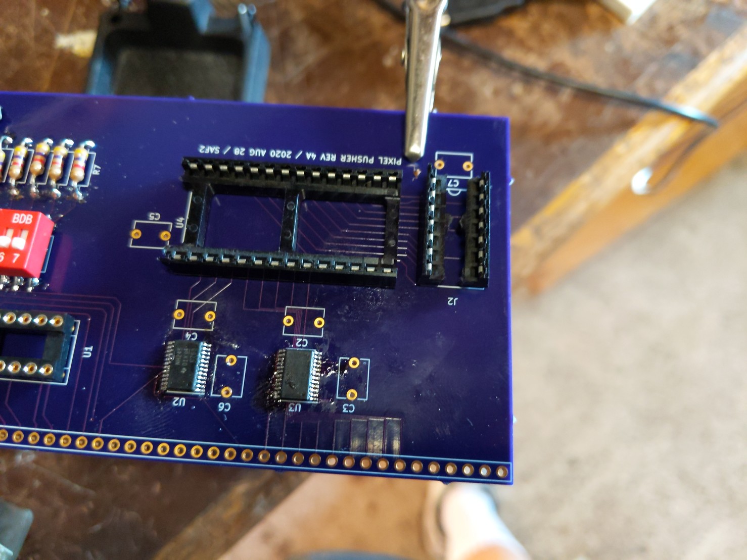
Of course, this socket is not intended to seat any chips; rather, it was intended to be used as the receptacle for a corresponding plug on a mezzanine board which included the analog bits of the interface. See my previous log entry for details on its pin-out (for video output purposes at least).
![]()
After installing the decoupling capacitors, I finally now had the means to install the bodge required to connect U2 to 3.3V supply.
This completes the soldering of the components onto the board. After soldering the 40-pin plug onto the board, the finished result looks really quite good, I must say.
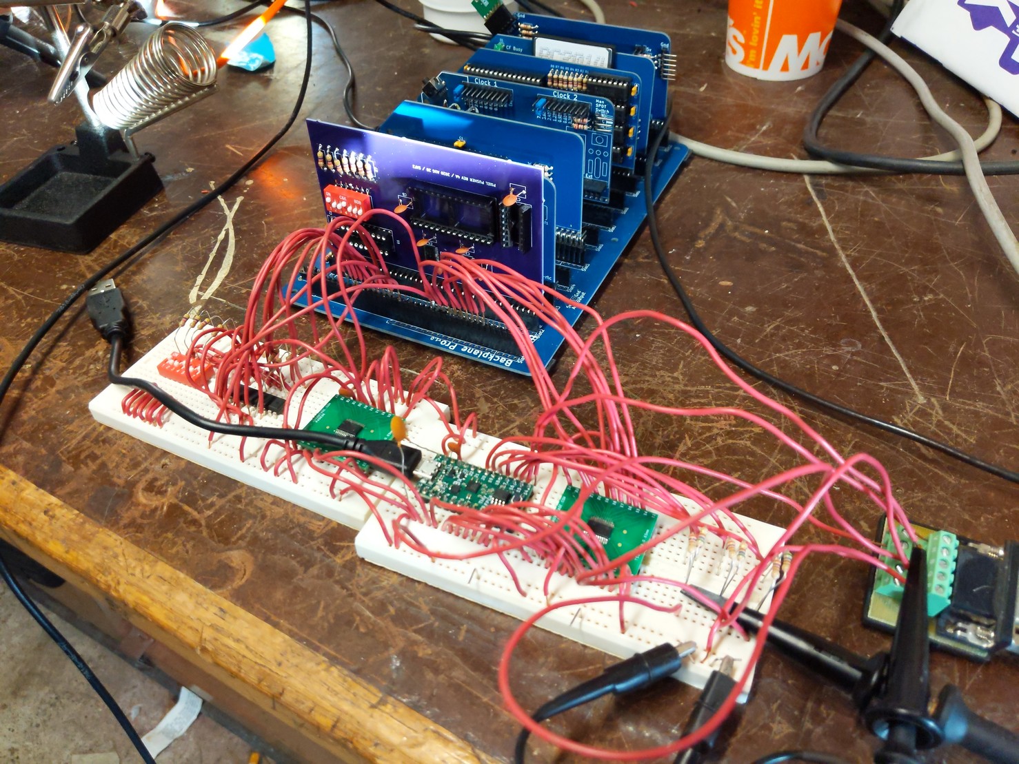
![]()
Here we see both the original breadboarded prototype of the circuit in the foreground, and immediately behind it (the only purple PCB there), we find the Pixel Pusher Revision 4A board sitting in the RC2014 backplane. These two circuits are (as far as my checks can confirm) electrically identical, so once I populate the Pixel Pusher card with a TinyFPGA BX and the 74HCT688 comparator chip, it should "just work" (where "work" is defined as the card should match the observed behavior, bug for bug and feature for feature, as the breadboarded circuit).
I ran out of time to perform testing; so, I'll need to wait until later to see how it performs.
-
Prototype PCBs ordered.
09/01/2020 at 23:53 • 0 commentsThat is all. ETA on delivery is September 11, but I probably won't get around to assembling one until some time after that.
-
PCBs Designs Finished
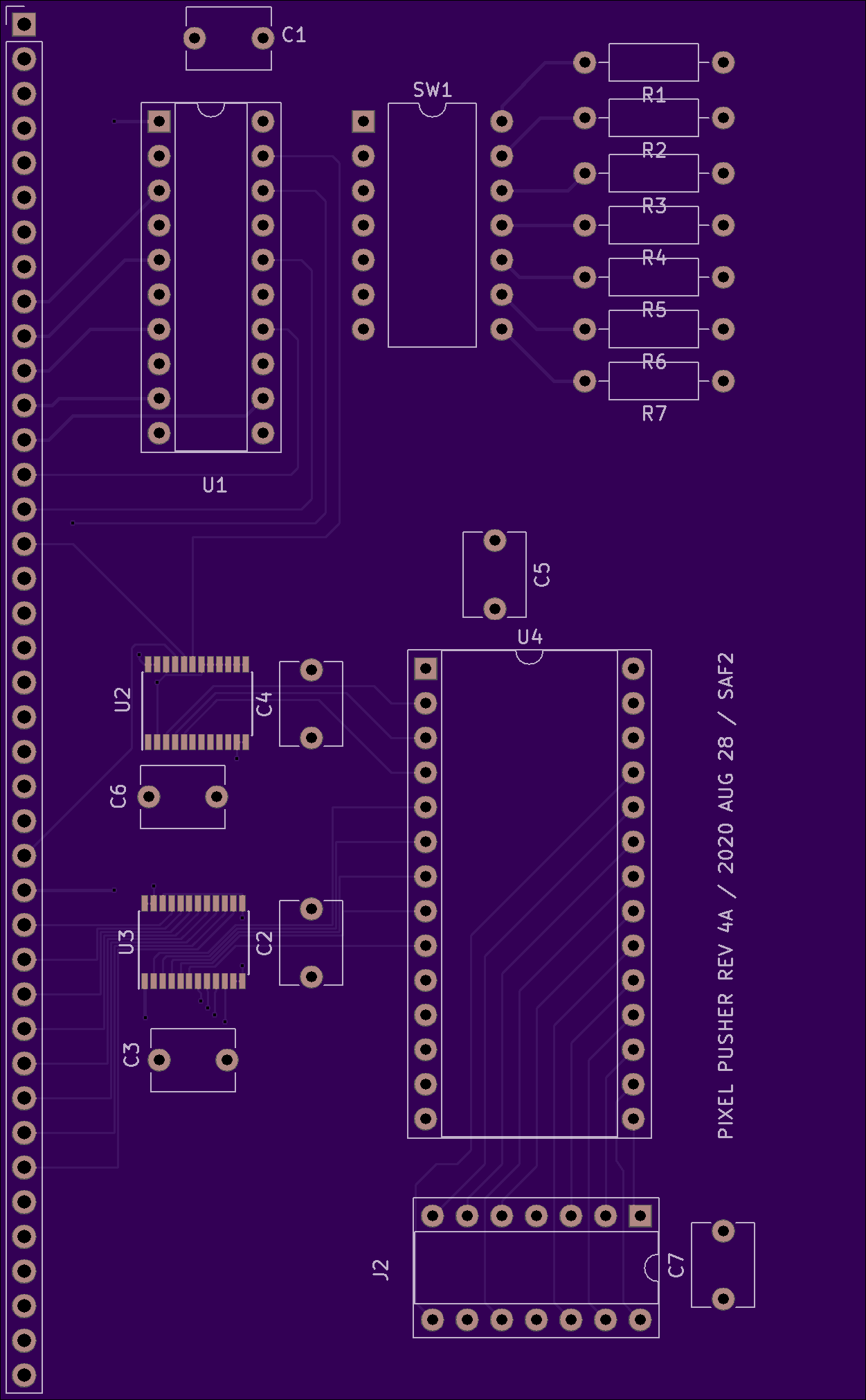
08/29/2020 at 02:02 • 0 commentsI've completed the initial design for the printed circuit boards for the RC2014 computer. This is my very first PCB design in KiCad, along with my very first 4-layer board, so I really have no idea what I'm doing. That said, I did it anyway, and the first batch of printed circuit boards have been submitted to OSH Park.
![]()
Nothing has been ordered yet, however. I'm waiting to hear back from OSH's support team on one question I had after uploading the designs. But, assuming everything checks out, I'll be placing an initial order for three circuit boards.
The circuit boards will make use of a 14-pin DIP socket as a connector for a mezzanine circuit board. This connector provides access to 11 digital I/Os on the FPGA, which is enough to drive an analog VGA port using discrete resistor DACs. The pin-out of the J2 connector (as it's currently labeled on the PCB) is as follows
| Description | Pin | Pin | Description |
|-------------+-----+-----+-------------|
| R2          |   1 |  14 | R1          |
| R0          |   2 |  13 | G2          |
| G1          |   3 |  12 | G0          |
| GND         |   4 |  11 | +3.3V       |
| B2          |   5 |  10 | B1          |
| B0          |   6 |   9 | n.c.        |
| HSYNC#      |   7 |   8 | VSYNC#      |
This pin-out supports a 512 color display. However, if you reprogram the FPGA for other tasks, it can be used to, e.g., control SPI or I2C devices, and so forth.
One pin is no-connect, and is intended to allow future mezzanine boards to auto-detect which version of the connector they're plugged into. For example, if a later revision of the video card supports 32768 colors, I'll need to add 6 more pins (at least). A 32K-color mezzanine designed for the 20-pin connector can still plug into and inter-operate with the older 14-pin connector, if it pays attention to pin 9. (Although, how it is to pay attention to pin 9 remains to be specified. YAGNI.)
-
Strip Buffers Done, VDC-II Core Usable (more or less)
05/30/2020 at 22:09 • 0 commentsI've completed the strip buffer implementation, the block memory arbiter, and the video fetch engine, and mated it with the MPE. This provides the host processor the ability to manipulate the display memory and we can finally observe the effects on the screen!
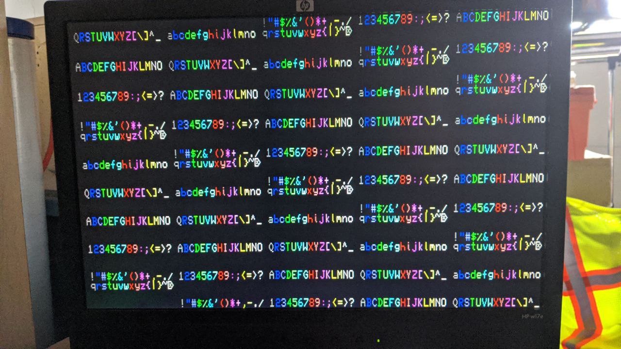
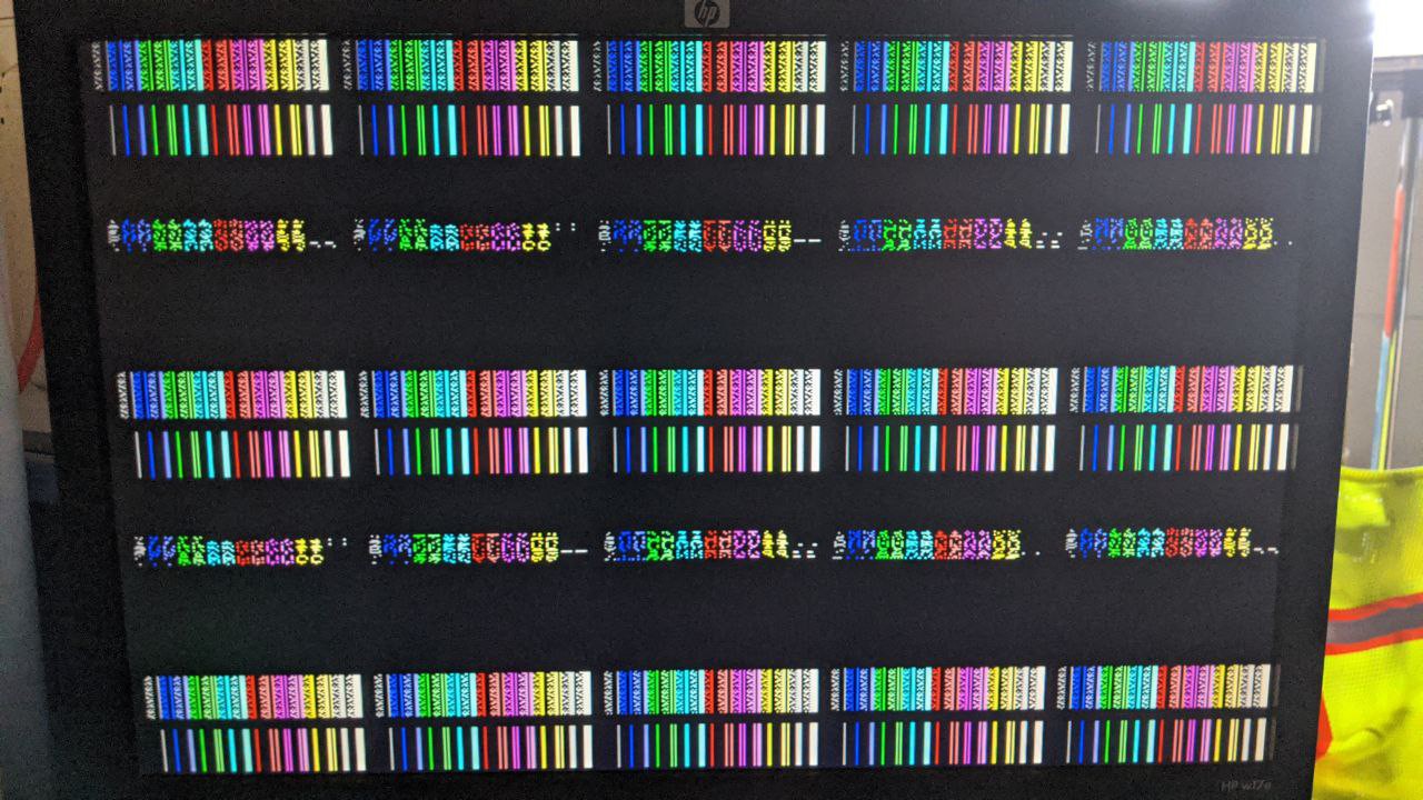
After setting the video mode to 80x30 text display, placing the text display at address 0000H and the attributes at 0C00H, you can run this little program in BASIC on the RC2014 to look at the first half of the VDC's character set (glyphs 0 through 255).
1000 OUT 110,18:OUT 111,0
1010 OUT 110,19:OUT 111,0
1020 OUT 110,31:FOR I=0 TO 2399:OUT 111,(I AND 255):NEXT I
1030 OUT 110,18:OUT 111,12
1040 OUT 110,19:OUT 111,0
1050 OUT 110,31:FOR I=0 TO 2399:OUT 111,(I AND 15):NEXT I
BASIC is slow enough that you don't need to worry about waiting for the MPE to finish stores into video memory; if you write this code in machine language, however, you'll need to remember to wait on the VDC. In any event, it should produce something resembling the following (if attributes are turned on).
![]()
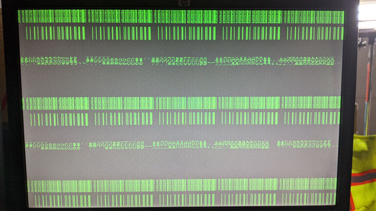
If you turn off the attributes and set the foreground and background colors to bright green and dark grey, you'll get a display which kinda sorta looks like a Commodore PET (or the Commodore 128 when it boots in 40-column mode).
Bitmapped graphics mode works as well. If you ran the previous code above, then try executing the following listing, you should see high resolution "garbage" on the screen, complete with color attributes applied. NOTE: the TinyFPGA BX is only big enough to contain 16KB of video RAM, as that's all the block RAM it has available. Thus, the 640x480 VGA display is going to have several repeated slices showing the same data. That's normal and expected.
OUT 110,25:OUT 111,INP(111) OR 128
![]()
Since the TinyFPGA BX only supports 16KB of RAM, there's no way to fit attributes in with a full-screen bitmap image. So, you'd typically turn off attributes to have a proper monochrome display. However, the VDC-II doesn't yet support scan-doubling, so it renders the screen at full resolution whether you like it or not.
OUT 110,25:OUT 111,INP(111) AND &HBF
OUT 110,26:OUT 111,&H51
![]()
Interesting how you can see where the screen data resides, where the attribute data resides, and where the character set resides in VDC memory. :)
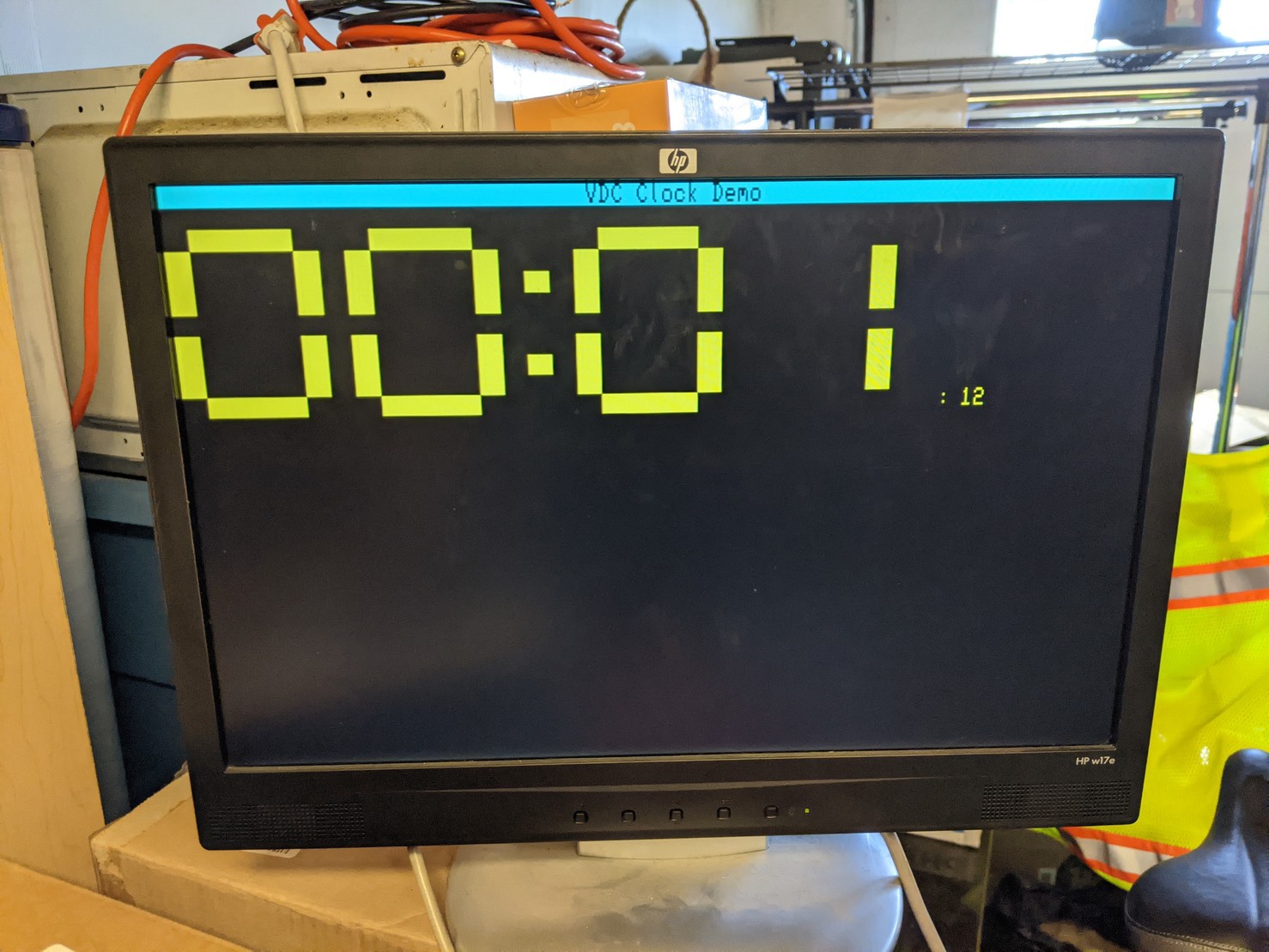
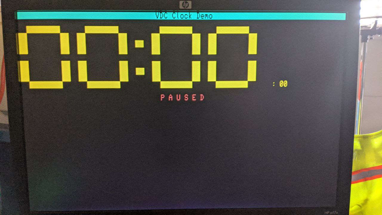
So, now that I've demonstrated that I have a workable, usable display, I figured it was time to try and write something that is "useful", in the sense that it is representative of a typical program most would consider to be useful. I decided to work on a simple clock application, and you can find the latest source code to it in the repository.
Here's what it looks like when it first starts up.
![]()
To unpause the clock, you tap the P key on the RC2014 terminal. It will then start counting up, in roughly 1 second intervals. Kinda sorta like this:
While working with the code, I ran into two hardware bugs. One of which I knew about from earlier development; however, a new bug has manifested. The bugs are:
- If polling the status register too fast, it will corrupt subsequent MPE operations. I've additionally discovered that this will even manifest when not using block-copy or block-write mode. It can also show up as corrupted VDC registers as well; it's not restricted to affecting video memory.
- And the latest bug I discovered was that, for some reason, reading the data register does not automatically update the update pointer. Thankfully, writes to this register does not cause issues.
What's Next?
In no particular order:
- Well, I'd like to finish the development of the clock; there are a few added niceties I'd like to throw in.
- I need to finish designing the printed circuit board for the VDC-II RC2014 card.
- Implement missing features, like hardware cursor, row address increment support, underline attribute support, etc.
- Fix known hardware bugs.
Still a ways to go before I can declare this project "done"; however, it's now certified to be in a usable state, which is quite exciting!
-
More Thoughts on Video Refresh
05/12/2020 at 16:22 • 0 commentsThe VDC video modes all assume that the VDC can access arbitrary video RAM with impunity. While you can fetch character and attribute data sequentially, resolving character codes to font data requires a potentially fresh hit to video memory, starting at either BASE+(16*code) or BASE+(32*code), depending on the configured character height.
Even if the character codes increase monotonically, the memory fetched will have 16- to 32-byte gaps in between referenced bytes. This breaks the optimal access pattern for synchronous memories, all of which are optimized for sequential access patterns. A good rule of thumb for synchronous memories is that every time you need to skip around in memory will cost you 10 cycles of latency.
Although it is possible to sequentially fetch character and attribute data, they occupy different segments of video memory, necessitating two video base pointers and two processing engines. Correspondingly, if you fetch 8 bytes of character data, you must also fetch 8 bytes of attribute data. The two bursts of data must be synchronized with each other externally to the memory fetch units.
Character and attribute bursts can happen in any order (e.g., attributes can be fetched ahead of character codes), but they must always be adjacent. Moreover, both character and attribute bursts must occur prior to font resolution, as attributes provide the 9th character code bit.
On the iCE40LP8K I'm currently targeting, a ping-pong line buffer, such as what I used to implement the MGIA on the Kestrel-2 and -2DX, will be prohibitively expensive. The space for a single line buffer of 256 characters would require 2048 DFFs (and, thus, logic elements). We would need two of these, so that the memory fetch logic can fill one buffer while the other is used for video refresh. Note that the FPGA only has 7680 logic elements.
Because they switch roles only on HSYNC boundaries, full-line buffers must be large enough to accommodate the widest display supported. The VDC-II register space supports 256 characters (all 8 bits of R1 are significant). If we couldn't accommodate a pair of line buffers large enough to support 256 characters, then we would need to ignore upper bits of register R1, which would break 8563 VDC compatibility.
Video data (resolved character/bitmap data plus corresponding attribute information) must be available when horizontal display enable asserts, since that's when we must start shifting out video data.
All of these problems interact. Thankfully, besides the queue-based approach I discussed in a previous log, there's another approach to work around these matters.
Another Solution
Instead of using full-line buffers, we use a pair of ping-pong "strip" buffers. Each strip is 4, 8, or 16 characters, depending mainly on externally imposed video memory latency requirements. For the purposes of this description, let's assume a 4-character strip.
A strip buffer contains two bytes for each character column it supports: an attribute byte and a bitmap byte. When attribute data is fetched, only the attribute bytes are updated. When character data is fetched, only the bitmap bytes are updated. The interface presented to the dot-shifter logic, however, always presents a 16-bit attribute/bitmap value pair.
To minimize the time needed to provide the complete set of data for a strip, attribute data should be fetched first. That way, when character data is fetched, we can stream data not only from video memory but also (in parallel) the strip buffer to provide the complete 9-bit character code to the font fetch unit. The font fetch unit can then resolve the character code to a bitmap byte. For this to work, font data must reside in fast FPGA block RAM.
The following table illustrates the memory fetch access patterns with 0-wait-state memory on a pipelined Wishbone B4 interconnect to video RAM and an asynchronous strip buffer read port. You could typically find this access pattern when placing character, attribute, and font data in block RAM. Assuming we reference video memory at the same speed as the dot-clock, we can reload the strip with video data in just 13 pixels. Note that a four character strip with 8 pixels per character contains 32 pixels, giving us ample time to refill the strip buffer. Four characters at 3 px/char would have only 12 pixels, so we would expect to see visual artifacts under those conditions. You'd want at least 4 px/char in order to ensure a clean display.
Cycle VRAM Address VRAM Data SBUF Read Address SBUF Write Address 1 ATTRPTR+0 2 ATTRPTR+1 a0 ATTR0 3 ATTRPTR+2 a1 ATTR1 4 ATTRPTR+3 a2 ATTR2 5 CHARPTR+0 a3 ATTR3 6 CHARPTR+1 ch0 CHAR0 7 CHARPTR+2 ch1 CHAR1 8 CHARPTR+3 ch2 CHAR2 9 FONT(ch0) ch3 PAIR0 CHAR3 10 FONT(ch1) bm0 PAIR1 CHAR0 11 FONT(ch2) bm1 PAIR2 CHAR1 12 FONT(ch3) bm2 PAIR3 CHAR2 13 bm3 CHAR3 Below illustrates the same refresh attempt, assuming that both attribute and character matrix data is located in a HyperRAM chip, while font data continues to be confined to block RAM. In this case, we see it takes 23 pixels to reload the strip buffer with video data, thanks to the HyperRAM access latency. As you might imagine, four characters of 4 pixels each will not be sufficient to refresh the display without artifacts. Therefore, if you intend on using a character-mode display with narrow characters, you should strive to keep the matrices inside VDC-II block memory space. Where possible, use external memory resources only for bitmapped video modes, or, make sure to use sufficiently wide characters.
Cycle VRAM Address VRAM Data SBUF Read Address SBUF Write Address 1 ATTRPTR+0 2 (wait) 3 (wait) 4 (wait) 5 (wait) 6 (wait) 7 ATTRPTR+1 a0 ATTR0 8 ATTRPTR+2 a1 ATTR1 9 ATTRPTR+3 a2 ATTR2 10 CHARPTR+0 a3 ATTR3 11 (wait) 12 (wait) 13 (wait) 14 (wait) 15 (wait) 16 CHARPTR+1 ch0 CHAR0 17 CHARPTR+2 ch1 CHAR1 18 CHARPTR+3 ch2 CHAR2 19 FONT(ch0) ch3 PAIR0 CHAR3 20 FONT(ch1) bm0 PAIR1 CHAR0 21 FONT(ch2) bm1 PAIR2 CHAR1 22 FONT(ch3) bm2 PAIR3 CHAR2 23 bm3 CHAR3 As long as the strip is wide enough to support the longest latency of the video memory, then we simply switch strip buffers after rendering the last pixel of a strip. Switching strip buffers should also commence fetching the next strip's worth of video data as well.
This algorithm should work to keep the video data sequenced for video refresh while it is in the middle of the scanline. The next issue to tackle is how to sequence the *first* strip, along the left-most edge of the display. The CRTC doesn't have enough information to trigger the first strip fetch exactly 4-16 characters ahead of the left edge of the display. The only events we can rely upon for this is:
- The negation of the display enable signal.
- The assertion of HSYNC.
- The negation of HSYNC.
I believe each of these events would serve a unique role. We would accumulate the address increment value to the fetch pointers when display enable falls. We would schedule the first strip fetch at the assertion of HSYNC.
Bitmap mode can be implemented by simply not resolving character codes into font bitmaps. "Monochrome mode" (that is, where one turns off attributes) can be implemented by having the attribute fetch logic just synthesize default attribute values based on register settings.
-
Thoughts on Handling Video Refresh
05/09/2020 at 01:14 • 0 commentsAt first, I thought the best approach to handling video refresh with the VDC-II core was to use ping-pong scanline buffers, like how the Kestrel-2's MGIA core did its video refresh.
I think that's still an approach that could work; but, I have to wonder if it wouldn't be simpler to just use a collection of modestly-sized queues instead?
At its core, a video controller consists of two parts: the timing chain (which I've already completed) and what amounts to a glorified serial shift register.
By its very nature, getting data from video memory to the screen happens in a very pipelined fashion. Everything is synchronized against the dot clock, and usually, also a character clock. Competing accesses to video memory, however, could cause a small amount of jitter; perhaps enough to cause visible artifacts on the display. Queues would apply naturally here, and can smooth out some of that jitter.
The disadvantage to using queues, though, is that video RAM access timing is much more stringent than with whole-line ping-pong buffers. I can't just slurp in 80 bytes of character data, 80 bytes of attribute data, and then resolve the characters into bitmap information (totalling 240 memory fetches), then sit around until the next HSYNC. I will need to constantly keep an eye on the video queues and, if they get too low, commence a fetch of the next burst of data.
The disadvantage to using ping-pong buffers, though, is a ton of DFFs and logic elements will go into making up the buffers. Like, if I want to support a maximum of 128 characters on a scanline (128 characters at 5 pixels/character can also provide a nice 640-pixel wide display), I'll need 384 bytes worth of buffer space: 128 for the character data, 128 for attribute data, and another 128 for the font data for each character on that particular raster. 384*8=3072 DFFs, and if memory serves, I think you need one LE per DFF. There are only 7680 LEs on the FPGA. I can't use block RAM resources because those are already dedicated for use as video memory (in this incarnation of the project, at least; I'll work on supporting external video memory in a future design revision).
So, while it's possible to implement a design using ping-pong buffers, it would make very inefficient use of the FPGA's resources. Since logic would be strewn all about the die, it could also introduce sufficient delays that the circuit fails to meet timing closure.
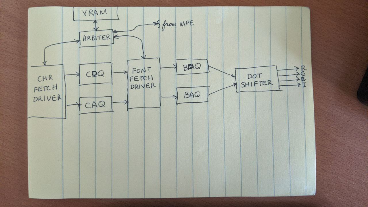
The more I look at things, the more I think using a set of fetch queues makes sense. I'm thinking a design similar to this would work:
![]()
Key:
- CDQ -- Character Data Queue
- CAQ -- Character Attribute Queue
- BDQ -- Bitmapped Data Queue
- BAQ -- Bitmapped Attribute Queue
Of course, I'm still not quite sure how to handle bitmapped graphics mode. The most obvious approach (which isn't always the best approach!) is to configure the font fetch driver to just pass through the data. But, this will require some additional though.
-
16KiB Video RAM, CPU Data Port Finished
05/08/2020 at 05:52 • 0 commentsI'm happy to report some progress made on the VDC-II project. I finished the CPU-to-video RAM interface. This includes block write and block copy functions from the original Commodore 8563 VDC chip. Only one small problem...
If you try to use the VDC-II chip as documented by Commodore, where you poke a register address, then wait for the chip to be ready, then poke a data value into a register, the DMA engine (what I call the Memory Port Engine, or MPE) corrupts video memory during a block operation.
However, if you poke the address, then poke the data, then wait on the ready flag, everything works perfectly! This breaks backward compatibility with Commodore's VDC, which makes me sad. It should work both ways; but, at least I have a viable software work-around.
Next steps are to implement the video fetch logic and the memory bus arbiter that will keep the different modules from stepping on each other's toes. If I can fix the aforementioned bug, that'd be great; but it's not a priority for me.
VDC-II
Commodore 8568-inspired (and mostly compatible) video core for driving VGA-type displays.