-
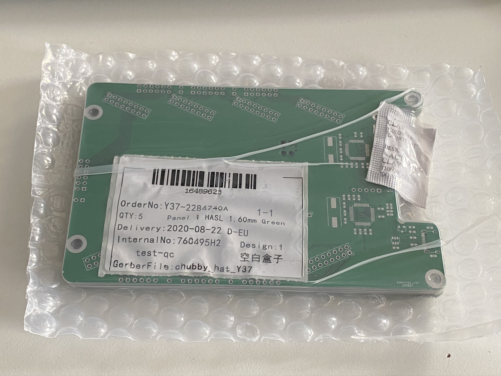
The boards arrived!
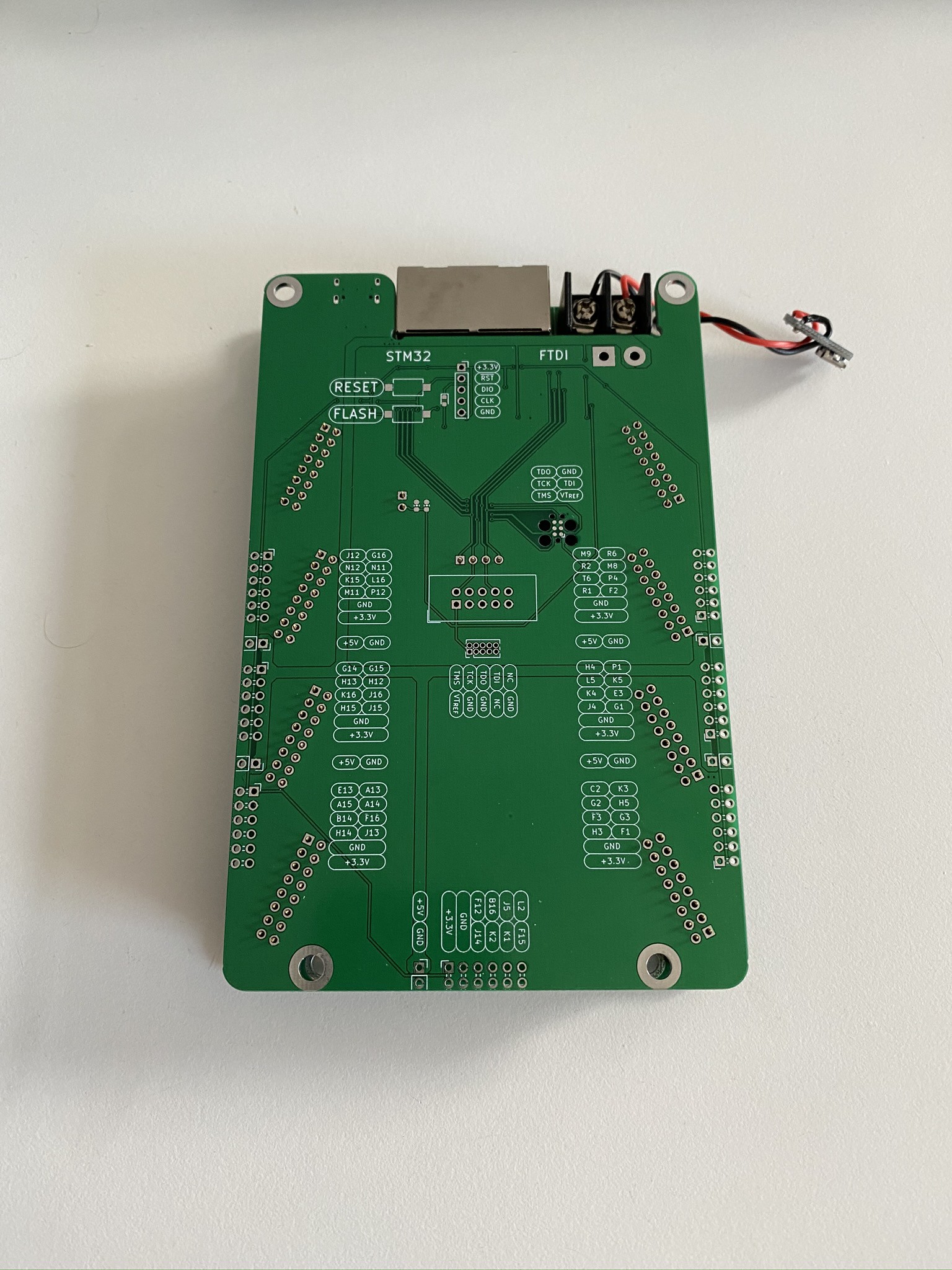
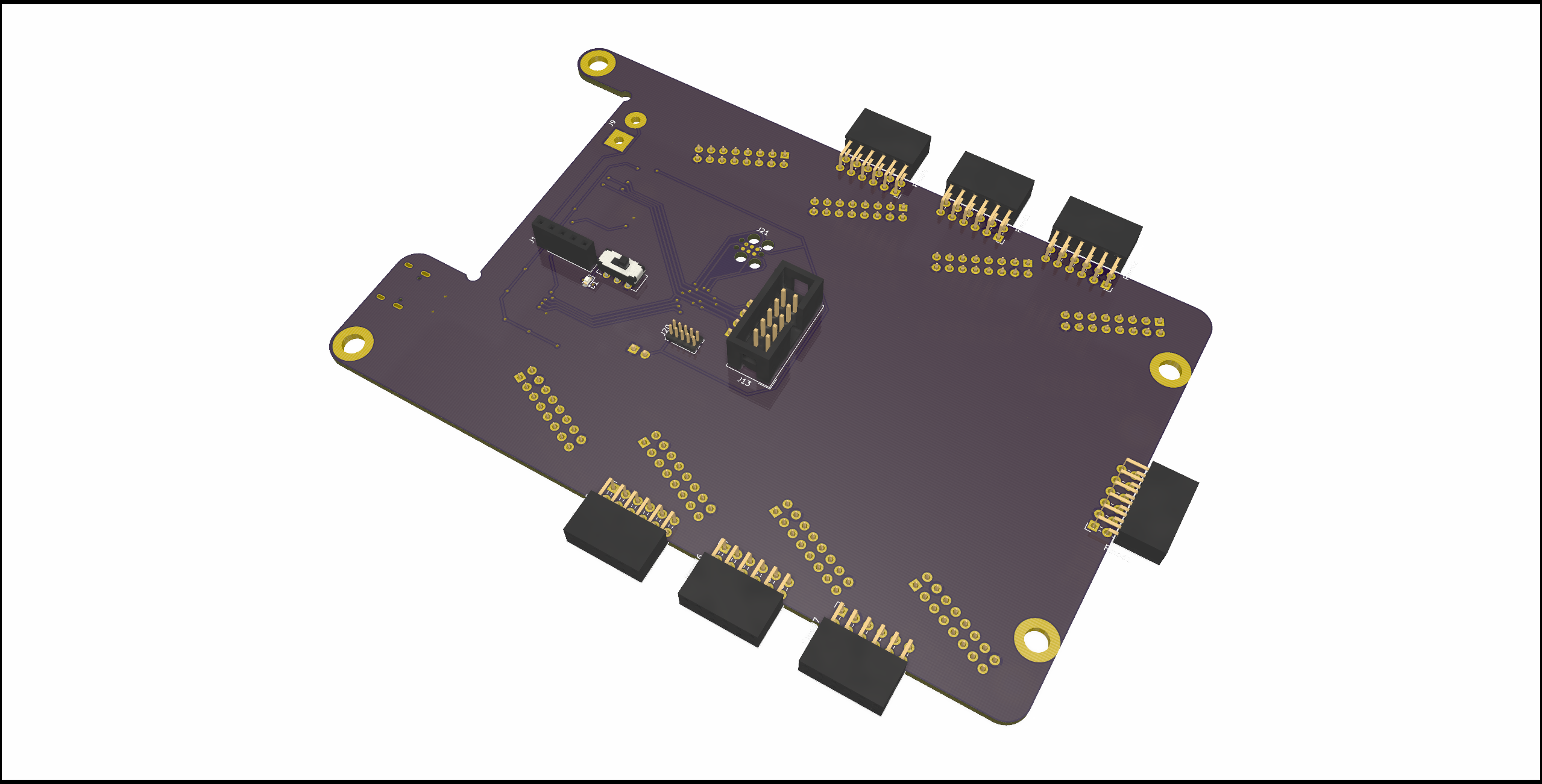
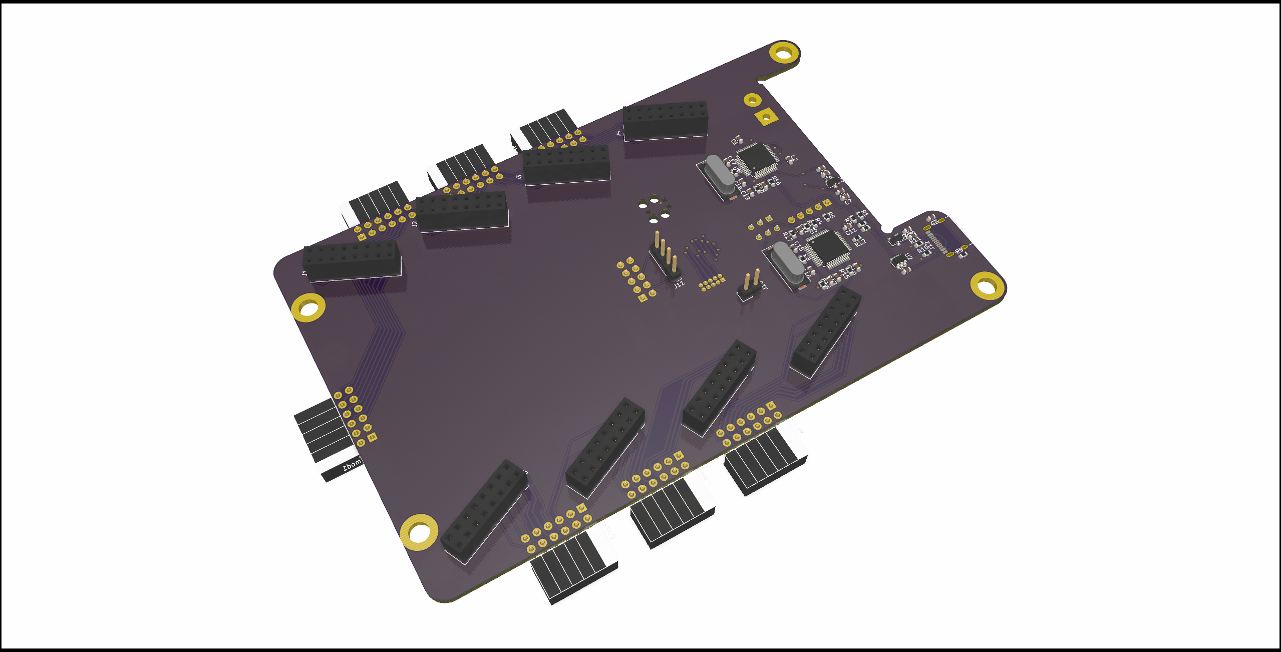
08/30/2020 at 17:10 • 0 commentsOn Friday the boards arrived. A quick test fit showed that all the contacts were properly aligned.
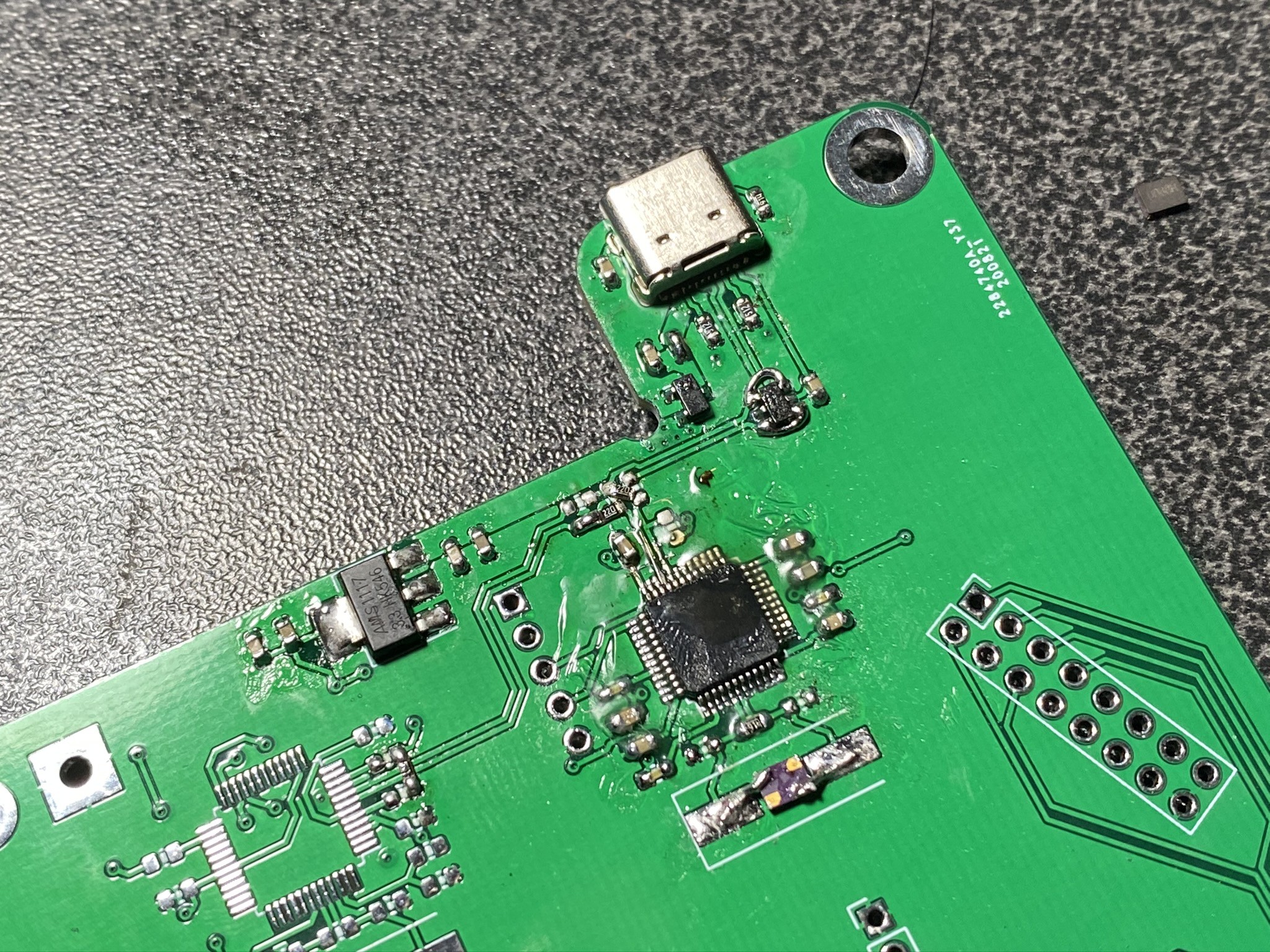
For some reason, the Type C receptacle on the first board I assembled went up in smoke after a wile. My computer didn't indicate a over current condition. Since the burnt spot was on the USB connector only and it seemed to have happened sporadically, I suspect that a rouge solder bubble might have been the cause.
My second attempt was more successful. Although I had double checked the schematic, I made the classic mistake of switching D+ and D- on the STM32. After some failed board surgery, I discovered that I can fix the problem by rearranging the resistors that are in series with the data lines.
I also wasn't patient enough to wait for the right parts to arrive. I desolderd the STM32 from a BluePill board and made some parts fit with wire.
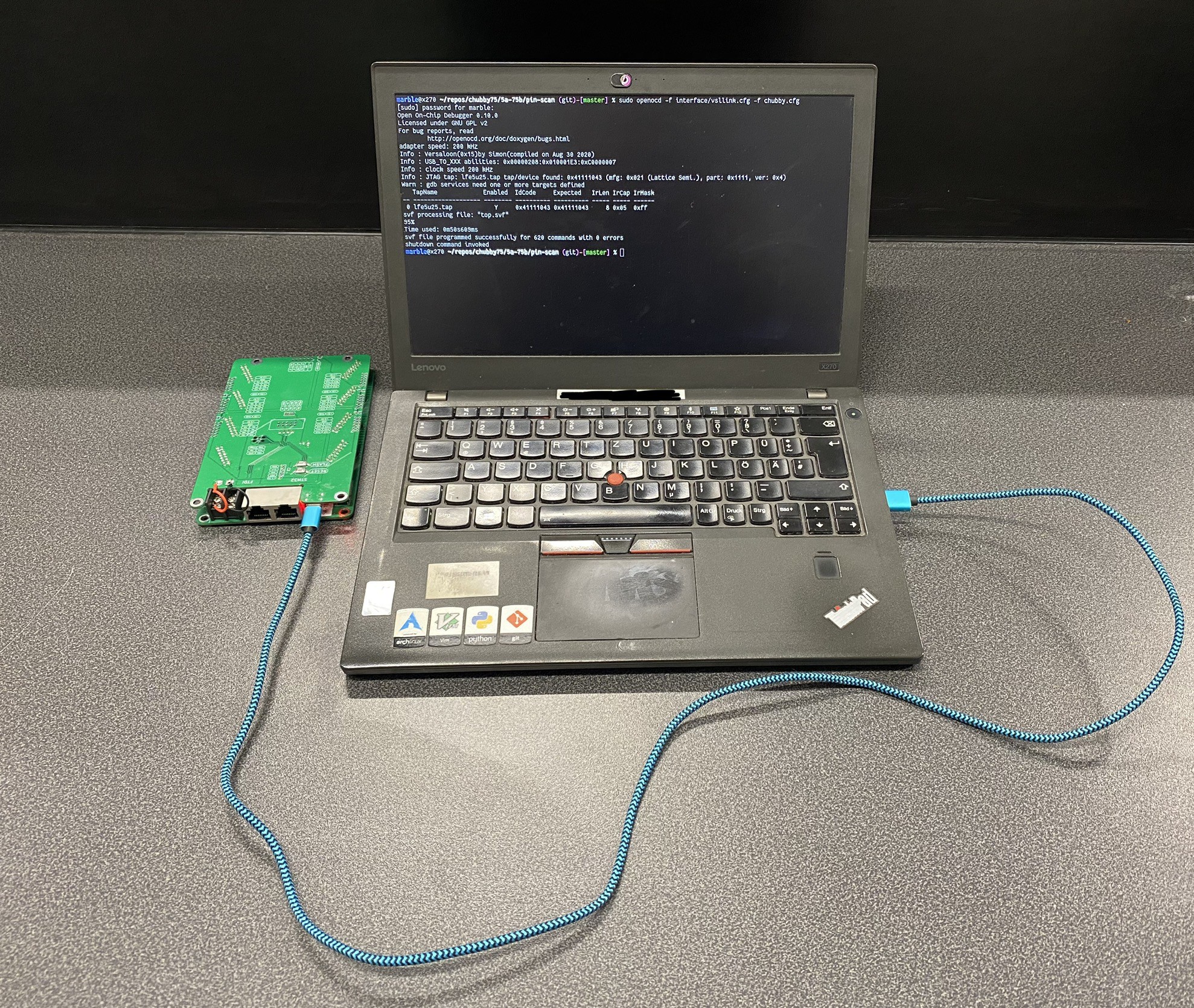
After finding and fixing the mistakes over the weekend I successfully flashed the versaloon firmware onto the STM32.
The are three bodges and a lot of flux on the board, but USB enumerated and that's all that mattered.
Finally I confirmed that all is working by programming the pin-scan bitstream on the FPGA.
-
Just Checking
08/19/2020 at 13:15 • 0 commentsBefore ordering PCB one should triple check everything. Apart from electrical rule cecking (ERC) the schemetic and design rule cecking (DRC) the layout, one should also check for mechanical fit.
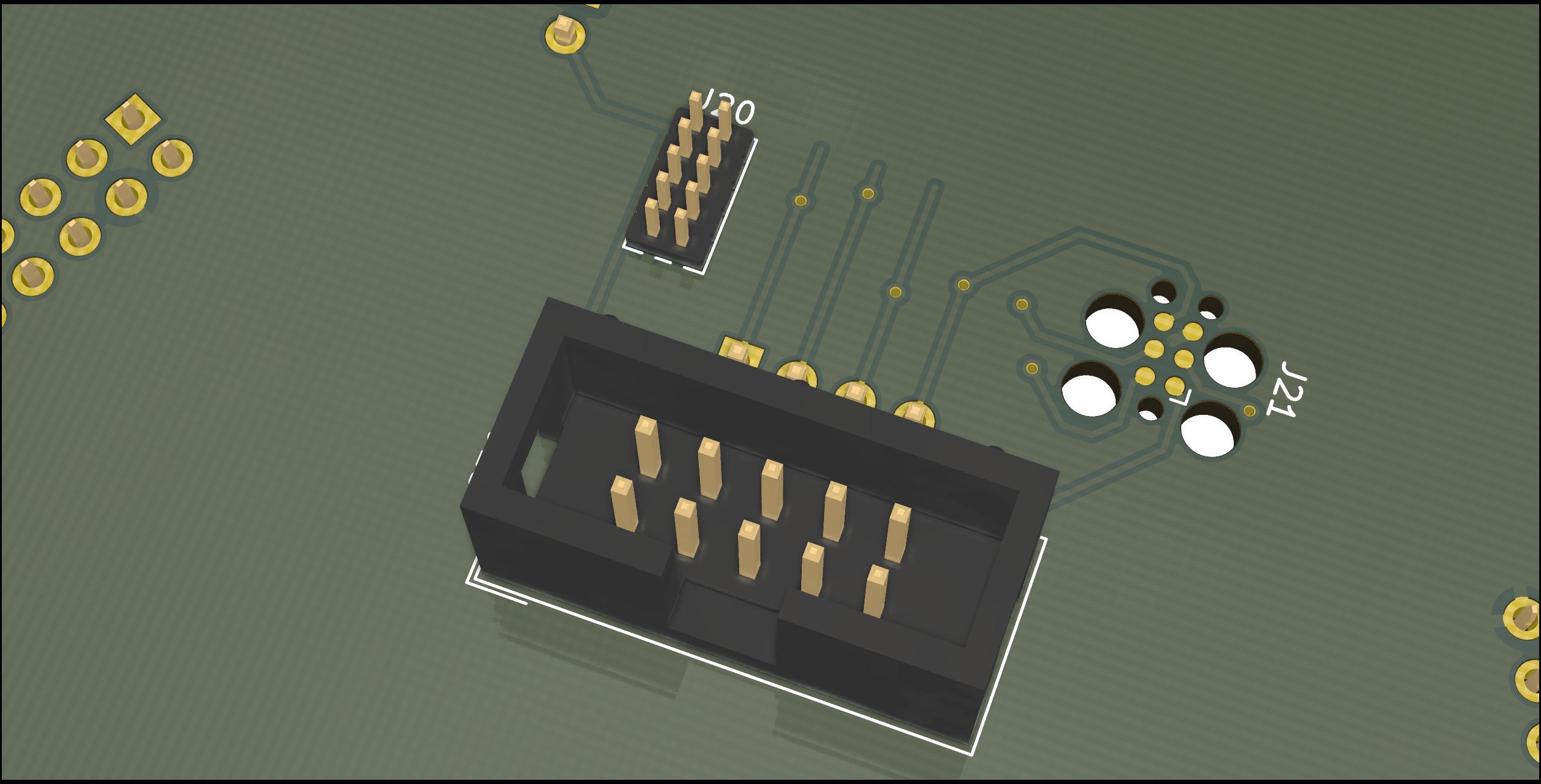
In our case we have to check that the connectors we placed on the board are in the right place with the right orientation. Usually, the latter is not as important, because designers tend to rotate parts in increments of 90 degrees. This is not the case with the HUB75 connector. They seem to deviate by 25 degrees from the 90 degrees reference.
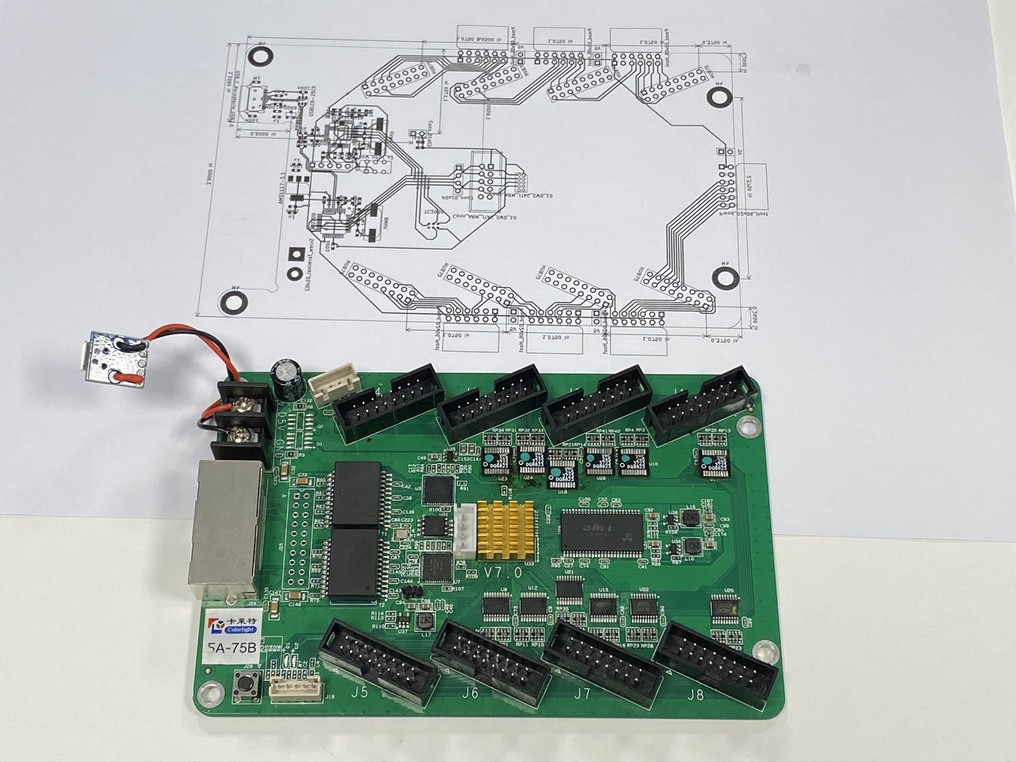
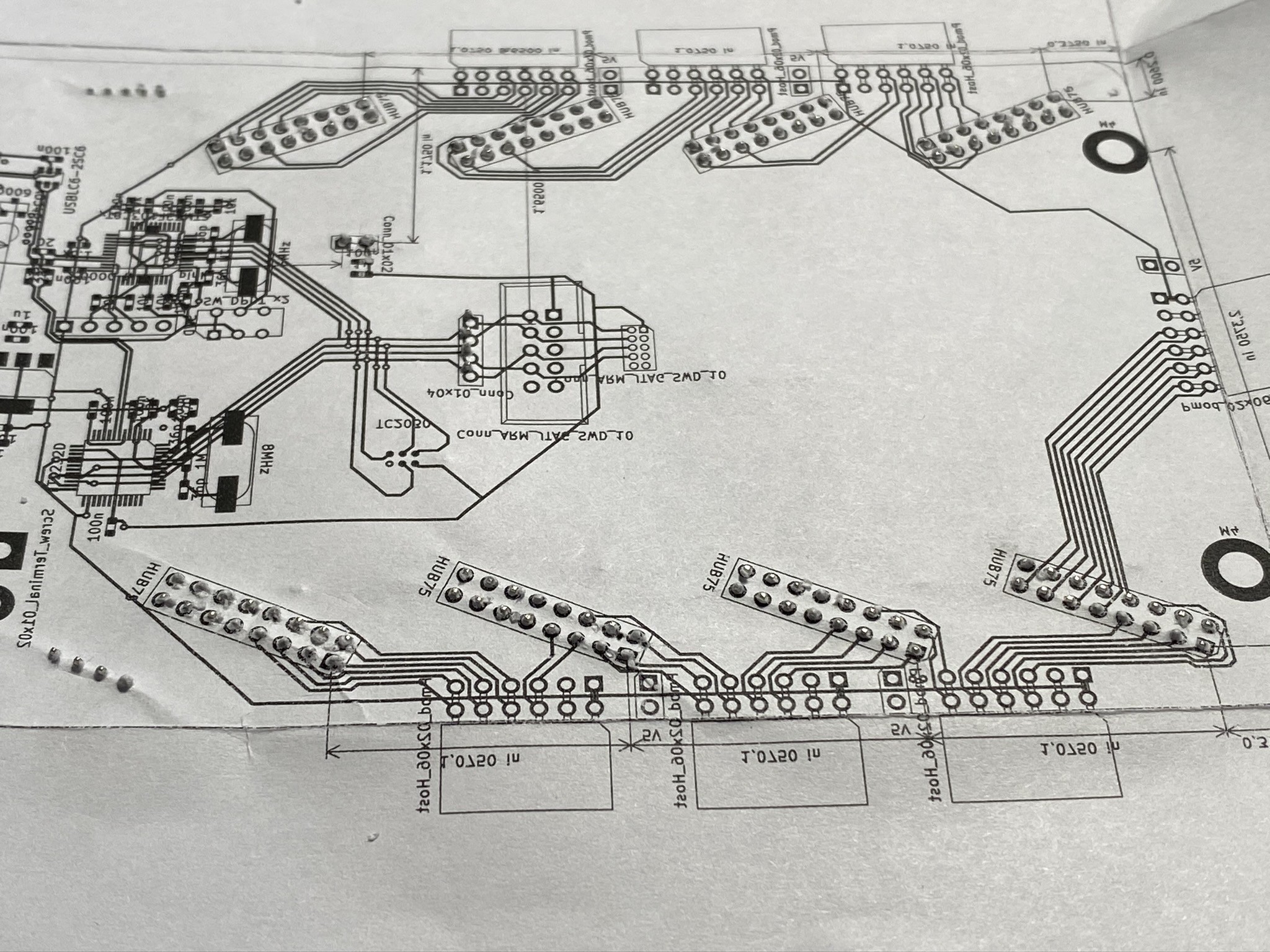
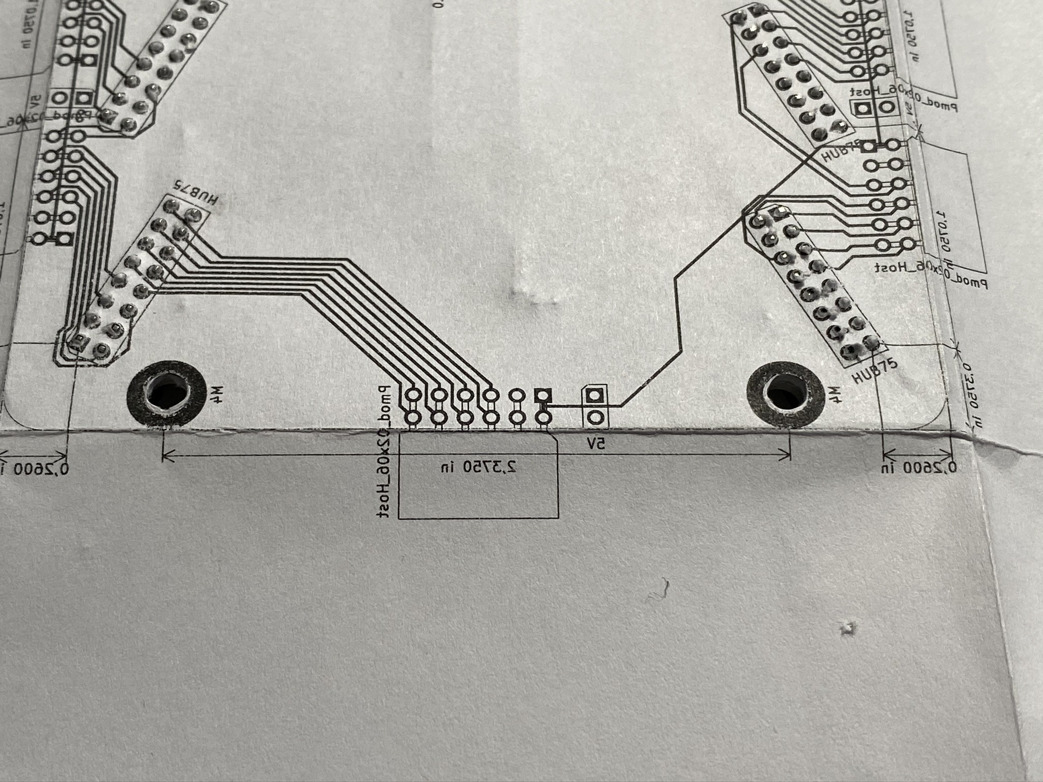
To test the placement and orientation I printed the layout on paper, since paper is way cheaper than PCBs and my printer has a quicker turnaround time that any fab - a trick I learned from Ben Heck.
![]()
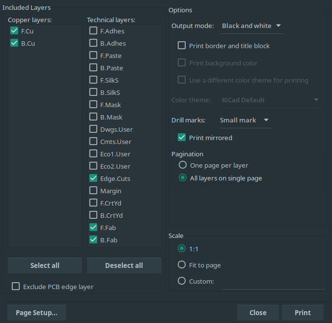
When printing one must pay attention to mirroring and scaling. The Colorlight has all its big through hole components on the top side. My design is also right side up. So I have to mirror the print if I want to use the bottom side of the Colorlight.
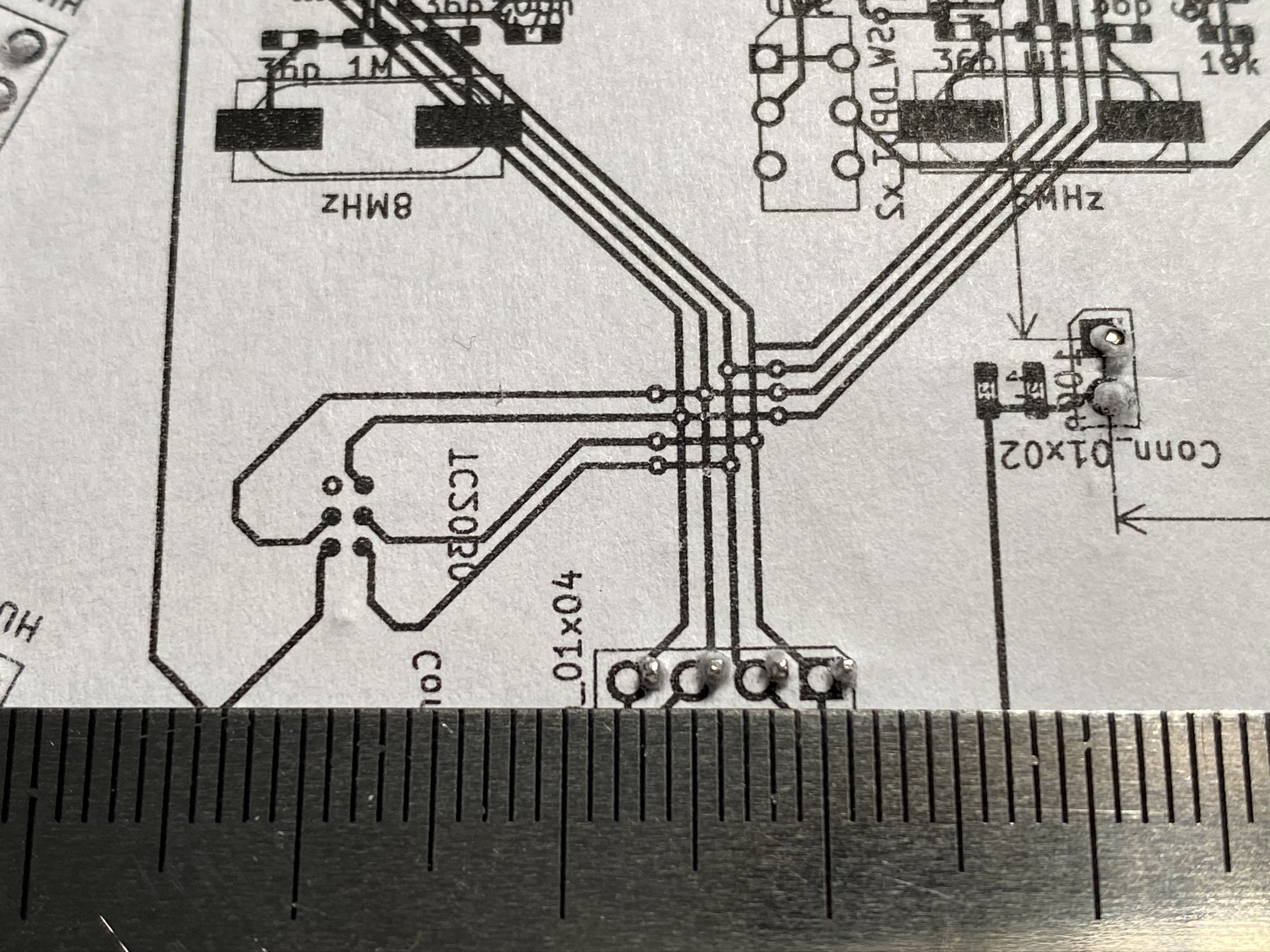
Scaling must always be 1:1. Pay attention to the printer dialog and check the printed page with a ruler.
Also clear all the copper pours from your design before printing (KiCAD: Ctrl+b) or your design will be mostly black.
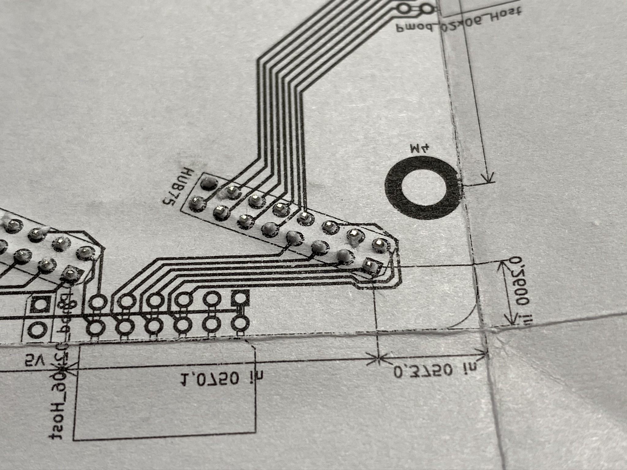
Getting the initial alignment right is tricky. In the future I might want to use translucent tracing paper. It also helps to fold along the edges and align the PCB with one corner. I then used my finger tips to find one pin through the paper, line it up with one pad on the paper and push through.
After that I aligned the connector on the opposite corner of the board and worked my way around all connectors.
Using a pen I also checked the alignment of the mounting holes.
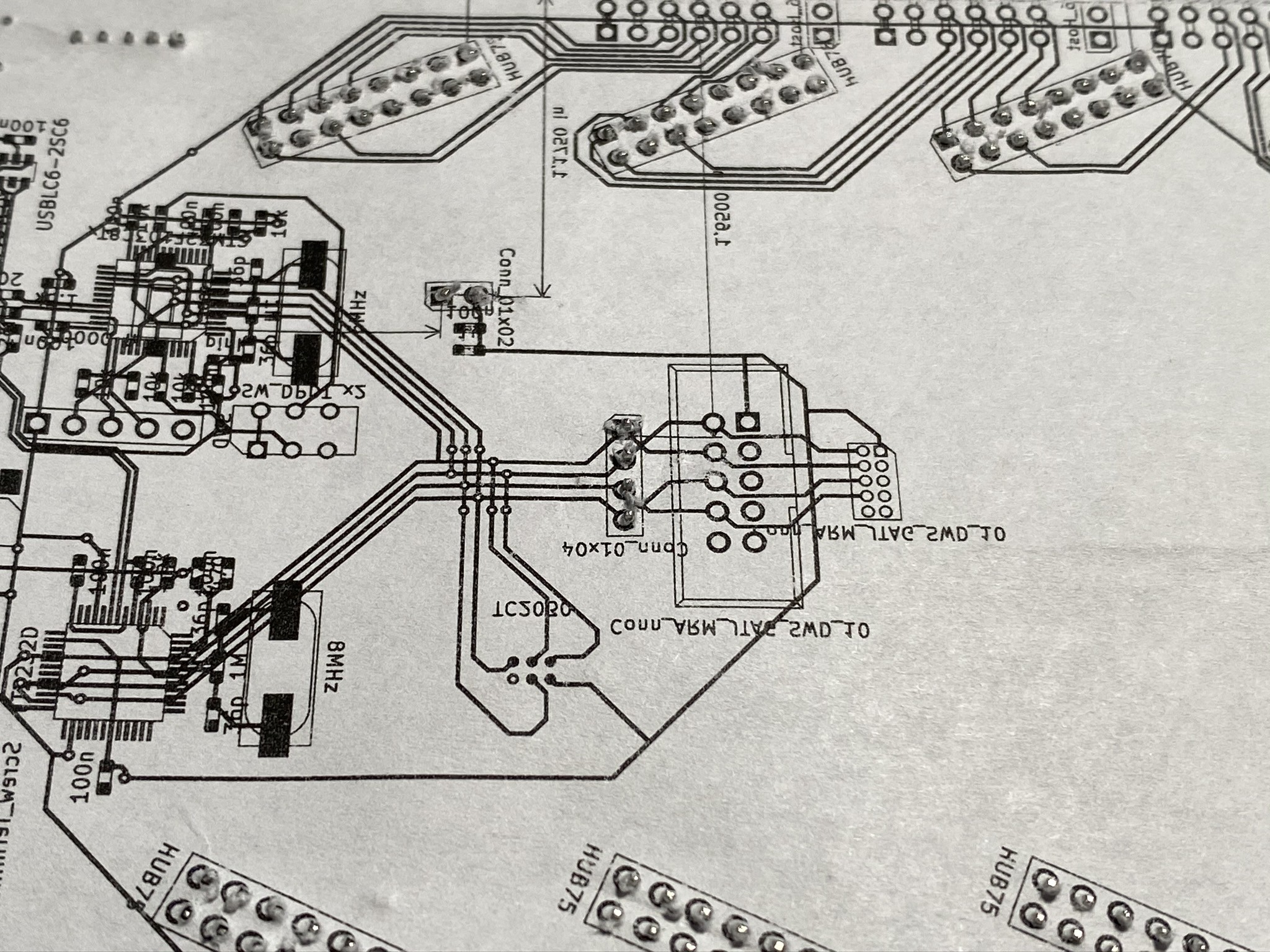
Everything looked nice, except for the JTAG header.
But after some adjustments, it also lined up well.
-
WIP
08/13/2020 at 16:09 • 0 commentsToday I got some more schematic design and routing done. The FTDI and versaloon programmer are implemented now. There still is silk screen cleanup and some more routing to do.
![]()
![]() I also sorted the schematic. It's very straight forward.
I also sorted the schematic. It's very straight forward.![]()
-
Going Cheaper
08/06/2020 at 20:11 • 0 comments9 minutes ago Arsenio Dev tweeted about using a FT232RL and openFPGALoader to program a Colorlight. On AliExpress you can find them for 0.64€/piece, which makes them even cheaper than the STM32 :D
-
Freedom of Choice
08/06/2020 at 14:08 • 0 commentsIn the last log I discussed replacing the FTDI with an STM32. Both approaches have their advantages and drawbacks and based on personal experience one might prefer one over the other.
To address that I decides to implement the FTDI circuit alongside the STM32 circuit. Simply populate only the component of the debugger you want.
Gladly both ICs require resistors in series with the USB data lines. This means that we can use these as switches, which makes an USB switch obsolete. It also prevents long "stub traces", that could compromise the signal integrity through reflections.
![]()
![]()
Other people again might already have a favorite on-chip debugger dongle and want to use that. For that case I added the three most common programming headers I could think of. Name the ARM JTAG header with 0.1 and 0.05 inch pitch, as well as TC2030.
![]()
-
Alternative to FTDI
08/01/2020 at 21:21 • 0 commentsThe icebreaker uses SPI to either write the bit stream to the non-volatile flash memory or directly to the FPGA. The bit stream written to the SPI flash gets automatically loaded by the FPGA after power-on.
The Colorlight also has a SPI flash holding the bit stream, but its pins are not exposed as headers. The contributors of the chubby75 repository identified the JTAG pins, which can also be used to program the bit stream into the FPGA.
This means that the bit stream we program only resides in the volatile memory of the FPGA, which deletes when the board gets powered off.
![jtag.jpg jtag.jpg]() https://github.com/q3k/chubby75/tree/master/5a-75b
https://github.com/q3k/chubby75/tree/master/5a-75bMost Lattice iCE40 development platform use a FTx232x for programming. This is a powerful IC because of its performance and versatility. It support most common protocols out of the box, like UART, I²C, SWD, SPI and JTAG. The latter two can be used to interface with iCE40 FPGAs.
In the hacker community FTDI got a pretty bad rep. There are not one, but two cases of FTDI releasing malicious drivers with the intention to brick counterfeit ICs. Apart from the moral of this, it also poses a risk to DIY hardware, since most hobbyist can't verify the genuineness of the parts we buy, especially from sites like Aliexpress.
Also their ICs are pretty pricey, starting at 4.18€/piece for 100 pieces when sourced on mouser and 2.50€/piece on AliExpress.
While searching for open source USB JTAG implementations, I stumbled upon this fork of versaloon, which ports it to the STM32F103C8 - the micro controller of the BluePill development board.
Apart from not being subject to malicious vendor driver, it's also relatively inexpensive. You can buy them on AliExpress for about 1€/piece. They probably are clones like the CS32F103, but as long as they work, they work 😃
I checked out v1.0 of the repository and flashed it to a blue pill board. After checking that the device get recognized by my computer with
dmesgandlsusb, I connected the JTAG signals and 5V power.![]() I tested the setup with the pin-scan example. Since I had a different version of the board than the author did, I hat to make some changes to the code.
I tested the setup with the pin-scan example. Since I had a different version of the board than the author did, I hat to make some changes to the code.diff --git a/5a-75b/pin-scan/Makefile b/5a-75b/pin-scan/Makefile index 2a870ce..a8978b6 100644 --- a/5a-75b/pin-scan/Makefile +++ b/5a-75b/pin-scan/Makefile @@ -7,7 +7,8 @@ top.json: $(SYNTH_SRCS) name.hex yosys -p 'read_verilog $(SYNTH_SRCS); synth_ecp5 -top top -abc9 -json $@' top.config: top.json top.lpf - nextpnr-ecp5 --25k --package CABGA381 --speed 6 --lpf top.lpf --json top.json --textcfg top.config --freq 65 + #nextpnr-ecp5 --25k --package CABGA381 --speed 6 --lpf top.lpf --json top.json --textcfg top.config --freq 65 + nextpnr-ecp5 --25k --package CABGA256 --speed 6 --lpf top.lpf --json top.json --textcfg top.config --freq 65 top.svf: top.config ecppack --input $< --svf $@ diff --git a/5a-75b/pin-scan/gen_lpf.py b/5a-75b/pin-scan/gen_lpf.py index 5b6d44f..365443c 100755 --- a/5a-75b/pin-scan/gen_lpf.py +++ b/5a-75b/pin-scan/gen_lpf.py @@ -15,7 +15,8 @@ with open(sys.argv[2], 'w') as lpf, open(sys.argv[3], 'wb') as rom: for l in cr: if not l[0].isdigit(): continue - if not l[7].isalnum(): + # if not l[7].isalnum(): + if not l[9].isalnum(): continue if l[1][0:2] not in ('PT', 'PB', 'PL', 'PR'): continue @@ -23,7 +24,7 @@ with open(sys.argv[2], 'w') as lpf, open(sys.argv[3], 'wb') as rom: continue name = l[1] - pad = l[7] + pad = l[9] lpf.write('LOCATE COMP "pads[%d]" SITE "%s";\t# %s\n' % (i, pad, name)) lpf.write('IOBUF PORT "pads[%d]" PULLMODE=UP;\n' % (i,))I also had to copy and modify an openocd config for the target platform
transport select jtag
adapter_khz 200

jtag newtap lfe5u25 tap -expected-id 0x41111043 -irlen 8 -irmask 0xFF -ircapture 0x05

init
scan_chain
svf -tap lfe5u25.tap -quiet -progress top.svf
shutdown
The programming is then done with OpenOCD.
$ sudo openocd -f interface/vsllink.cfg -f chubby.cfg
Open On-Chip Debugger 0.10.0
Licensed under GNU GPL v2
For bug reports, read
    http://openocd.org/doc/doxygen/bugs.html
adapter speed: 200 kHz
Info : Versaloon(0x15)by Simon(compiled on Jul 26 2020)
Info : USB_TO_XXX abilities: 0x00000208:0x010001E3:0xC0000007
Info : clock speed 200 kHz
Info : JTAG tap: lfe5u25.tap tap/device found: 0x41111043 (mfg: 0x021 (Lattice Semi.), part: 0x1111, ver: 0x4)
Warn : gdb services need one or more targets defined   TapName             Enabled  IdCode     Expected   IrLen IrCap IrMask
-- ------------------- -------- ---------- ---------- ----- ----- ------ 0 lfe5u25.tap            Y     0x41111043 0x41111043     8 0x05  0xff
svf processing file: "top.svf"
95%
Time used: 0m50s625ms
svf file programmed successfully for 620 commands with 0 errors
shutdown command invoked
Inititally I had some troube with the length ot the wires I used and the stupied way of routing them through the opposing holes for strin relief. At
adapter_khzvalues over 10 I got JTAG error. probably due to bad signal integrity.I got rid of that by shortening the wires and not doing the strain relief thing.
-
The Ins and Outs
07/29/2020 at 15:01 • 0 commentsThe biggest problem with the Colorlight is that all signals going to the HUB75 are going through 74HC245 octal bus transceiver, which direction pins are hardware to configure them as output.
Sadly, lifting the direction pin and configuring the transceivers as input would damage the FPGA with 5V, as discussed here. One could also lift the power supply pin of the IC and supply 3.3V instead of 5, but that would turn a whole bank of FPGA pins into input-only pins, which IMO defies the versatility of an FPGA.
![image image]()
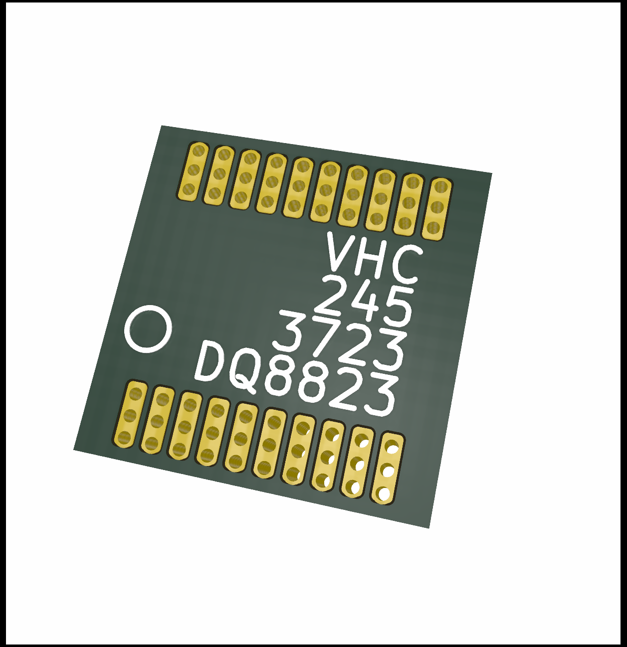
My current approach is to de-solder the transceiver ICs and replacing them with bridge. The bridge is simply a PCB that connects each input to its corresponding output.
Ideally the boards would simply be castellated holes and traces connecting each input to its corresponding output.
I'm not the first one having ytrouble at this point. The problem is that the pitch of the tranceiver IC is so fine that no fab would accept the design. My guess is that the router bit would simply rip out the plating of the castellated holes if the drill diameter is too tiny.
![]()
Due to this problem I had to go through some design iterations until I arrived a something that was accepted by the fab.
This design is essentially the footprint of the transceiver IC with the aforementioned traces, and holes through the pads.
The holes on one hand server the purpose wicking up excess solder, but also help aligning the PCB with the footprint on the Colorlight.
Chubby Hat
This projects goal is to design a PCB that turns the Colorlight 5A-75B into an easy to use development platform for cheap.
 marble
 After finding and fixing the mistakes over the weekend I successfully flashed the versaloon firmware onto the STM32.
 I also sorted the schematic. It's very straight forward.



 I tested the setup with the
