Close
0%
0%

25 A Supercapacitor Charger

Higher current, still air supercapacitor charger

Public Chat
Similar projects worth following
Parallel MOSFET implementation of a supercapacitor charger with 25A current. Also, uses a super cool planar inductor.

I wanted to extend the learning that I had done on my 6 Amp supercapacitor charger, and push it to 25A.  Here is the previous project:

https://hackaday.io/project/174806-supercapacitor-rapid-charger

The main goal of the project is to increase the charging current, yet still be able to run the charger in still air.  Side goals included using a nifty planar inductor and changing over to an ATMEGA328PB.

Here is the whole setup on the bench:
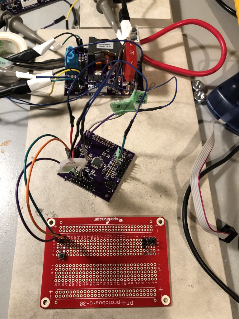
At the top is the 2 oz perfect purple PCB that carries the switching MOSFETs, inductor, 50A fuse (safety!), driver and current amplifier.

The middle board is an ATMEGA328PB evb that I designed (20 MHz external clock, and voltage dividers/filters for the comparator and analog to digital converters).

The bottom breakout board is the "chicken button".  When you press the button, the 328PB executes the charging code.  When you release the button, the 328PB stops.  I was playing with higher charging currents and different parameters, so sometimes the switching MOSFETs can get a little warm, and you want to be able to stop the charging if things start to go into thermal runaway.

The first thing to test is applying the charging current to a wire (when the supercapacitor is completely discharged, it will act like a short circuit).  Here is the oscilloscope view of passing the ~25 A through the wire.

The top two traces are the switching voltages (channel 1 for the high side MOSFETS, channel 2 for the low side MOSFETs).  Channel 3 is the voltage at the input to the inductor.  Channel 4 is the current amplifier output.  The current sense resistor is 300 uOhm, the amplifier gain is 200, and output voltage of the current sense amplifier is ~1.5 volts.  So, 25A is flowing through the wire.  The ATMEGA328PB is controlling the current by monitoring the current amplifier output using the comparator.  If the comparator output is low (indicating the current is too high), the controller will decrease the inductor current by increasing the "on-time" of the low-side FET.  If the comparator output is high, the controller will increase the inductor current by decreasing the "on-time" of the low-side FET.

Here is the lab video showing the charging of a 450 F supercapacitor.  You know the charging is done, because the capacitor hissing stops!  The ATMEGA328PB shuts down the charging when the capacitor voltage is about 2.8 V (this is a 3 V supercapacitor, but I wanted a bit of margin).

To charge the supercapacitor from 0.67 V to 2.81 volts takes approximately 40 seconds, so the average charging current is about 24 amps.  

  • 1 × PQ3218-6R0-50-T Planar inductor
  • 1 × ATMEGA328PB Microcontroller

  • Code for the ATMEGA328PB

    sciencedude199010/30/2020 at 15:35 0 comments

    Here is the code for the ATMEGA328PB

    Here is the code for the ATMEGA328PB
    
    #include <avr/io.h>
    #define F_CPU 20000000UL // Use external 20 MHz clock, set to external oscillator in the fuses
    #include <util/delay.h>
    
    const uint8_t MAX_CAP_VOLTAGE = 145; // Assume output of cap is more or less at ADC
    const uint8_t START_CAP_VOLTAGE = 130; // When to start charging - hysteresis
    
    const uint8_t COUNT_FET_DEFAULT = 0; // When starting to charge, the lower FET on time
    const uint8_t COUNT_LOW_DEFAULT = 200; // The starting count for all switches off
    
    // Enumerated type for the state machine
    typedef enum {IDLE, CHARGING, STOP} state_var;
    
    int main(void)
    {
        // Variable to hold the state
        volatile state_var the_state = IDLE;
        
        // The low side on time
        uint8_t count_fet = COUNT_FET_DEFAULT;
        
        // The idle time when everything is low
        uint8_t count_low = COUNT_LOW_DEFAULT;
        
        // PB0 for V high (high side)
        // PB1 for V low (low side)
        // PB2 for trigger
        DDRB = 7;
        PORTB = 0;
        
        //DDRD = 255 - (1 << 5);
        
        // Setup the analog comparator, set bandgap reference (instead of AIN0)
        ACSR = (1 << 6);
        
        // Setup the ADC (use AVCC, left adjust, and ADC0 as the input)
        ADMUX = (1 << 6) + (1 << 5) + 0;
        
        // Enable ADC, start it up, auto trigger, divide by 128 for prescalar
        ADCSRA = (1 << 7) + (1 << 6) + (1 << 5) + 7;
        
        // Free running mode
        ADCSRB = 0;
        
        // At start, just wait in case of issues with programming
        _delay_ms(3000);
            
        while (1) {
            
            if ((PIND & (1 << 5)) == 0) {
                the_state = STOP;
            }
                    
            if (the_state == IDLE) {  // Idle state
                
                // Wait to let the ADC readings settle
                _delay_ms(3);
                
                if (ADCH < START_CAP_VOLTAGE) { // Begin charging
                    // Initialize lower FET on time
                    count_fet = COUNT_FET_DEFAULT;
                    count_low = COUNT_LOW_DEFAULT;
                    
                    // Update state variable
                    the_state = CHARGING;
                }
            }
            else if (the_state == CHARGING) { // Charging state
                
                for (uint8_t qq = 0; qq < 128; qq++) { // Cycles of current control
                    // Charging loop
                    // Turn on the high side FET
                    PORTB = 1 + 4;
                    PORTB = 1;
                    PORTB = 1;
                    PORTB = 1;
                    PORTB = 1;
                    PORTB = 1;
                    PORTB = 1;
                    PORTB = 1;
                    PORTB = 1;
                    PORTB = 1;
                    PORTB = 1;
                    PORTB = 1;
                                            
                    // Turn off the high side FET, prevent shoot-through
                    PORTB = 0;
                    PORTB = 0;
                    PORTB = 0;
                    
                    // Turn on the low side FET
                    for (uint8_t jj = 0; jj < count_fet; jj++) {
                        PORTB = 2;
                    }
                    
                    // Turn off the low side FET, all low
                    PORTB = 0;                
                    for (uint8_t jj = 0; jj < count_low; jj++) {
                        PORTB = 0;
                    }
                            
                    if ((ACSR & (1 << 5)) == 0) { // Current too high                    
                        if (count_fet < 255) {
                            count_fet = count_fet + 1;
                        }                    
                    }
                    else { // Current too low
                        if (count_fet > 0) {
                            count_fet = count_fet - 1;                    
                        }
                    
                        if (count_low > 0) {
                            count_low = count_low - 1;
                        }
                    }
                }
                if (ADCH > MAX_CAP_VOLTAGE) {
                    // Done charging, set to IDLE
                    the_state = IDLE;
                }                                    
            }    
            else if (the_state == STOP) {
                PORTB = 0;
                _delay_ms(1);
                if ((PIND & (1 << 5)) == (1 << 5)) {
                    the_state = IDLE;
                }
            }                
        }
    }

View project log

Enjoy this project?

Share

Discussions

sciencedude1990 wrote 12/31/2020 at 06:00 point

if you have low Vgs- how many transistors are you driving from the TI part?  If you have something like two or three, maybe there isn’t enough drive strength?  What is the total gate charge?

  Are you sure? yes | no

sciencedude1990 wrote 12/23/2020 at 13:55 point

As for debugging - I placed debug points all around PCB.  These are the headers labelled "TP4", "TP2", etc.  Each testpoint has a signal, and a ground.

See

https://hackaday.io/project/174806-supercapacitor-rapid-charger/log/184205-scope-probin

  Are you sure? yes | no

sciencedude1990 wrote 12/23/2020 at 13:53 point

Hi Julian - thanks!  The testbed (https://hackaday.io/project/174806-supercapacitor-rapid-charger) was based on a Bourns SRP1265A inductor.  Depending on your switching speed, and resolution/speed of the controller, this inductor would be fine at higher currents.  You just have to pick the correct inductance, and possibly add some kind of cooling (since the package is a little small).  The chart in the SRP1265A datasheet has the saturation current, so you have to stay lower than that (possibly including the "ripple" current that extends higher than your average current).  The Standex Meder inductor was just too cool looking to pass up for the higher current design!

The same goes for the transistors - the PowerPAK SO-8 Single are fine up to about ~8 Amps in still air and a 2 oz PCB.  Higher than that, and you have to add some kind of cooling (heat sinks, forced air, etc.).  So, I paralleled them to get to 25 A.

I didn't look in detail at the BQ24640, but did do a design and test with the LT3741.  Look to page 13 and on in the LT3741 datasheet - there are detailed calculations of which inductor value to select.

Another important aspect is the selection of the input capacitors.  I used ceramic, paralleled capacitors.  Why?  Because with the ripple current, the capacitors will start to heat up too.  They are a bit noisy though.

As for layout, take a look at the photo of the partially assembled PCB: 

https://hackaday.io/project/175638/gallery#a480eaaaa1984f3a10330b35579b26b0

I made all the paths extremely short, and rotated the components to fit together on a small board (see the sense resistor).  I did a Kelvin connection on the sense resistor - kind of a must for 0.0003 Ohm resistors.  All of the current path connections were copper zone fills.

I pushed this board up to 50A, but in still air, it heats up too quickly.

  Are you sure? yes | no

julian.straub wrote 12/24/2020 at 02:02 point

Thanks for your thoughts! Initially I definitely had the wrong inductor with a saturation current that was too low. The latest iteration also uses the Bourns SRP :). I am following the guidelines from the datasheet. 

I am using SiR460DP for the switches which should be rated high enough but I am not sure how to accurately determine how hot they get. 

I am also using paralleled input and output capacitors of 10uF each. The total amount according to the datasheet. How high were your individual capacitances?

I did try to keep all paths short. The paths for the gate connections of the power MOSFETs did get a bit long with a via each though (1cm each). Probably still short enough.

One thing that is confounding to me is that somehow the Gate-Source voltage only reaches 2V instead of the 6V which it should have according to the datasheet. Not sure why?? I did try to keep the ground plane wide and big...

I was measuring things with a short circuit cable as you show it as well. Since I never got the desired currents, I was wondering if its something the IC is doing? Some kind of gentle start or something. So I just connected a supercap and voila now it seems to be reaching the desired current rating! 

Fixing the inductance seems to have worked. It also seems I needed to not short circuit the output for testing. I might have to go back and measure the GS voltage again now with the supercap at the output. 

  Are you sure? yes | no

julian.straub wrote 12/24/2020 at 02:18 point

MMmm the GS voltage of about 2.1V at a drain current of 6A (which is what I am currently charging at) do follow the relationship between V_GS and I_D as shown in the datasheet. https://www.mouser.com/datasheet/2/427/sir460dp-93818.pdf

I am not 100% sure (maybe somebody can confirm?) but it seems like by fixing the drain current the "on" GS voltage is also determined. So because the MOSFET does not need to be folly on for 6A drain current, I am seeing the 2.1V GS voltage? 

  Are you sure? yes | no

sciencedude1990 wrote 12/24/2020 at 04:26 point

I might guess that they measure the change in capacitor voltage versus time.  The short circuit testing I did was only for demonstrating the ideas.  Since I made my own controller, it was tolerant to the short circuit.

Is the bandwidth on your scope set low - are you measuring the average VGS?  If it is 2.1V and the current is 6A, looking at the datasheet I would think you would be dissipating ~2W in the transistor because of the relatively high RDS at that bias.  Or, are you saying the peak VGS is 2.1V, and the signal out of the controller is still PWM?

I think my total capacitance was 220 uF.  Each cap was a 22 uF, 25V, 1206.

  Are you sure? yes | no

julian.straub wrote 12/29/2020 at 19:31 point

I am seeing a nice PWM signal with a maximum of about 2.1V for the high part of the signal. The frequency is correct.  Pretty weird. I think Ill post to the TI forum.

  Are you sure? yes | no

julian.straub wrote 01/03/2021 at 06:16 point

I figured it out - all is well and working. I had a error in my measurement setup. This is what it was for https://hackaday.io/project/176654-candle.

  Are you sure? yes | no

julian.straub wrote 12/21/2020 at 18:53 point

Very cool project :). I wonder why you abandoned the other charger? No way to push it to higher currents?
I have been experimenting with the BQ24640 but somehow cannot get beyond 3A charging current. Any specific learnings on how to design the high current paths or what to look for in the inductors? How do you go about debugging the circuit?

  Are you sure? yes | no

Similar Projects

Does this project spark your interest?

Become a member to follow this project and never miss any updates