 Anton Poluektov
-
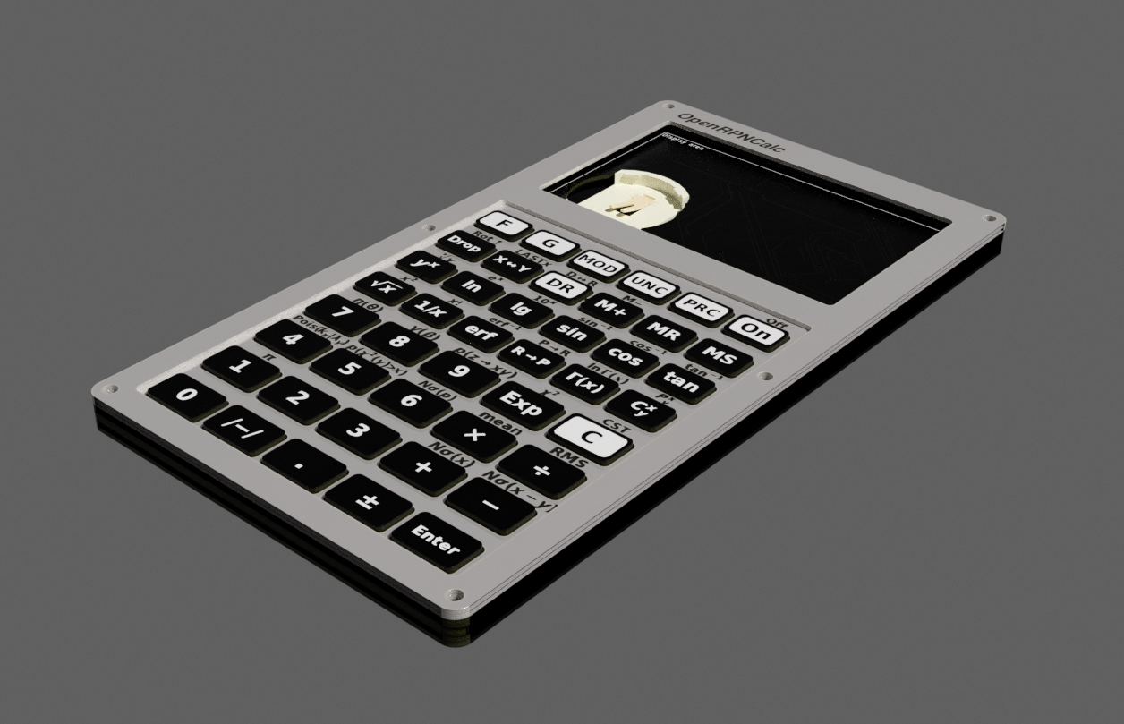
Revision 4.0 is out
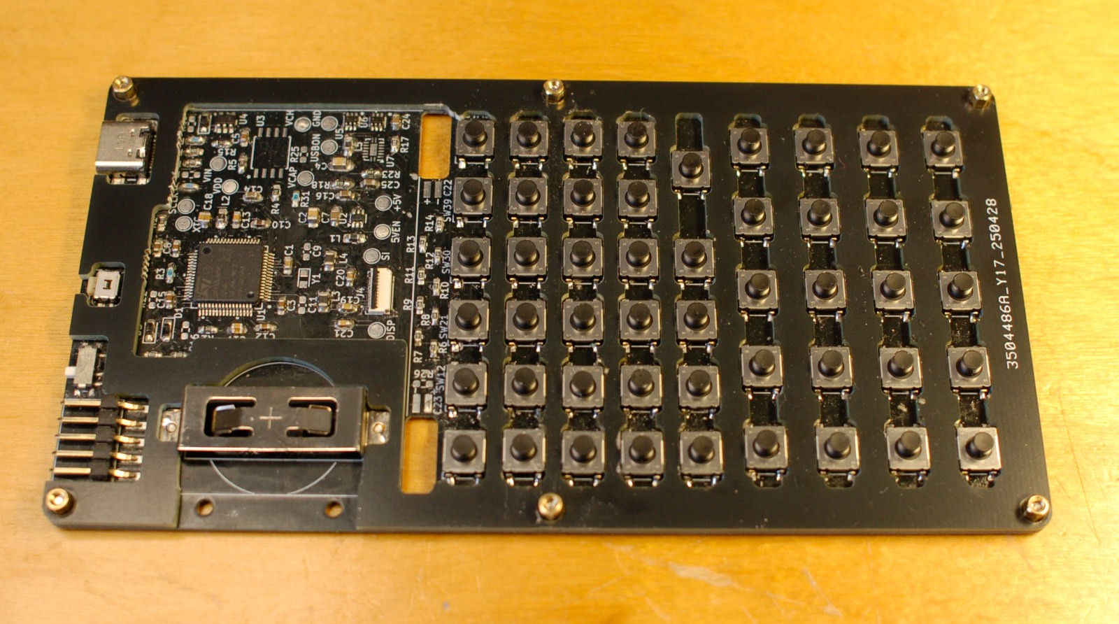
05/29/2025 at 21:15 • 0 commentsI've assembled rev 4.0, the version with the newest STM32U385 chip and 49-key keyboard. As usual, all the design files are available on OpenRPNCalc github.
![]()
The firmware is mostly the same for now, just adapted to the new MCU chip and with minimal modifications to the keyboard layout to use 49 keys. However, with the hardware improvements (USB-C, flash and a more powerful MCU), we can aim to eventually support DB48x firmware.
Welcome jcordona on board, he is trying to build rev 4.0 with third-party PCB assembly. If anybody else is brave enough to join this effort, welcome to the github discussion thread.
-
Revision 4: WIP
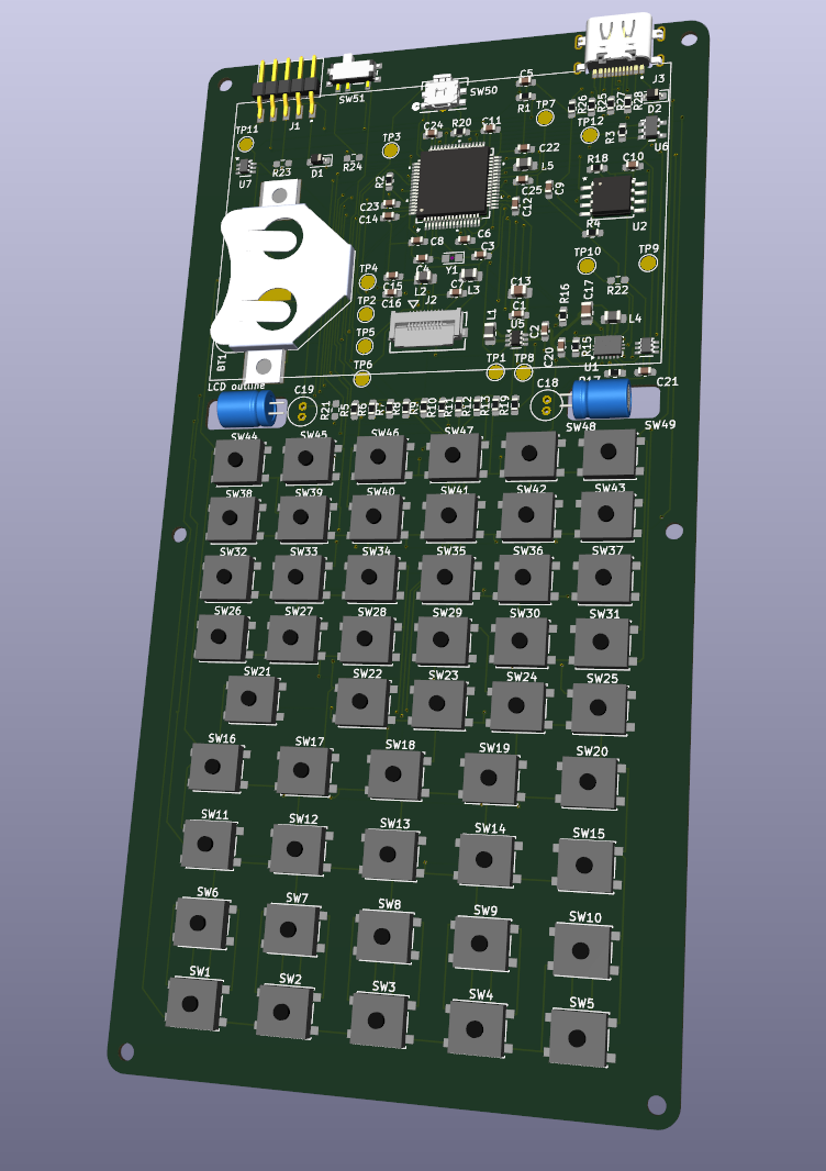
04/11/2025 at 14:58 • 0 commentsWorking on revision 4:
Most recent STM32U385 processor with SMPS and 10 uA/MHz consumption
- 8MB flash
- Optimised coin cell power circuit based on NBM5100 chip and supercaps to flatten out current spikes during flash activity
- Additional row of function keys a la HP48
- Back to single PCB layout (soldering keys and flat cable connector to aluminium PCB is a pain!)
-
Keycaps and an issue with PCB service
03/22/2025 at 11:32 • 0 commentsI had one issue with the well-known cheap PCB service I wanted to ask the community for help with.
My ultimate goal is to make a design that looks nice, but at the same time is cheap and easy to reproduce in small amounts (of course, one can make the custom silicon keypad, but will be cheap only in large amounts, given the engineering fee). That's why I'm experimenting with PCB+slikscreen for keycaps.
Now, the PCB that produces the top parts of my keycaps looks like this:
![spacer2_3d.png]() It's a usual FR4 PCB with a black mask and white silkscreen that would cost you a few bucks in a typical cheap PCB prototyping service. The problem is, my service insists this is a panelised PCB with 44 different designs in it (why not 45, don't they count the frame?) so they ask like 20 times more for this one compared to the other boards of the same size. I agree it's a bit of a stretch to call this a PCB, as it requires a lot of milling and so on, but x20, come on!
It's a usual FR4 PCB with a black mask and white silkscreen that would cost you a few bucks in a typical cheap PCB prototyping service. The problem is, my service insists this is a panelised PCB with 44 different designs in it (why not 45, don't they count the frame?) so they ask like 20 times more for this one compared to the other boards of the same size. I agree it's a bit of a stretch to call this a PCB, as it requires a lot of milling and so on, but x20, come on! Has anybody had experience with it? Can you recommend a service with a more flexible policy? I guess Aisler would do this cheaper because they claim they charge simply proportional to the PCB area, but sadly they don't have a black mask option, and in any case, I'd need to order the rest elsewhere since they don't do Alu PCBs and two-layer 0.8mm thickness.
-
Changes in Rev. 3
03/13/2025 at 22:28 • 0 commentsThe code and design files for Rev. 3 are now available on github.
In terms of schematics, there are no major changes. The most significant one is the addition of external 1M pull-ups (instead of 40k internal for STM32) to reduce the current consumption when a key is being pressed. There is also a mechanical switch to choose the source of power between the battery cell and ST-LINK probe (or to completely power off the circuit if ST-LINK is not connected).
The PCBs and enclosure, however, are significantly modified to make the whole thing much slimmer. I've switched to the thinner CR2016 battery instead of CR2032 and a matching low-profile battery holder. The keyboard switches and the battery are now soldered to a separate single-layer aluminium PCB which at the same time serves as the back lid: this allowed me to shave off another couple of millimeters from the case thickness. The overall thickness of the enclosure is now slightly under 7 mm, which probably makes this device the slimmest RPN calculator out there! The main PCB and keyboard/battery PCB are connected by a flex cable.
![]()
(of course I screwed up the layout of the keyboard PCB, so you see some red wires that needed to be added to fix it. This bug is now corrected in the github repository.)
-
OpenRPNCalc rev.3
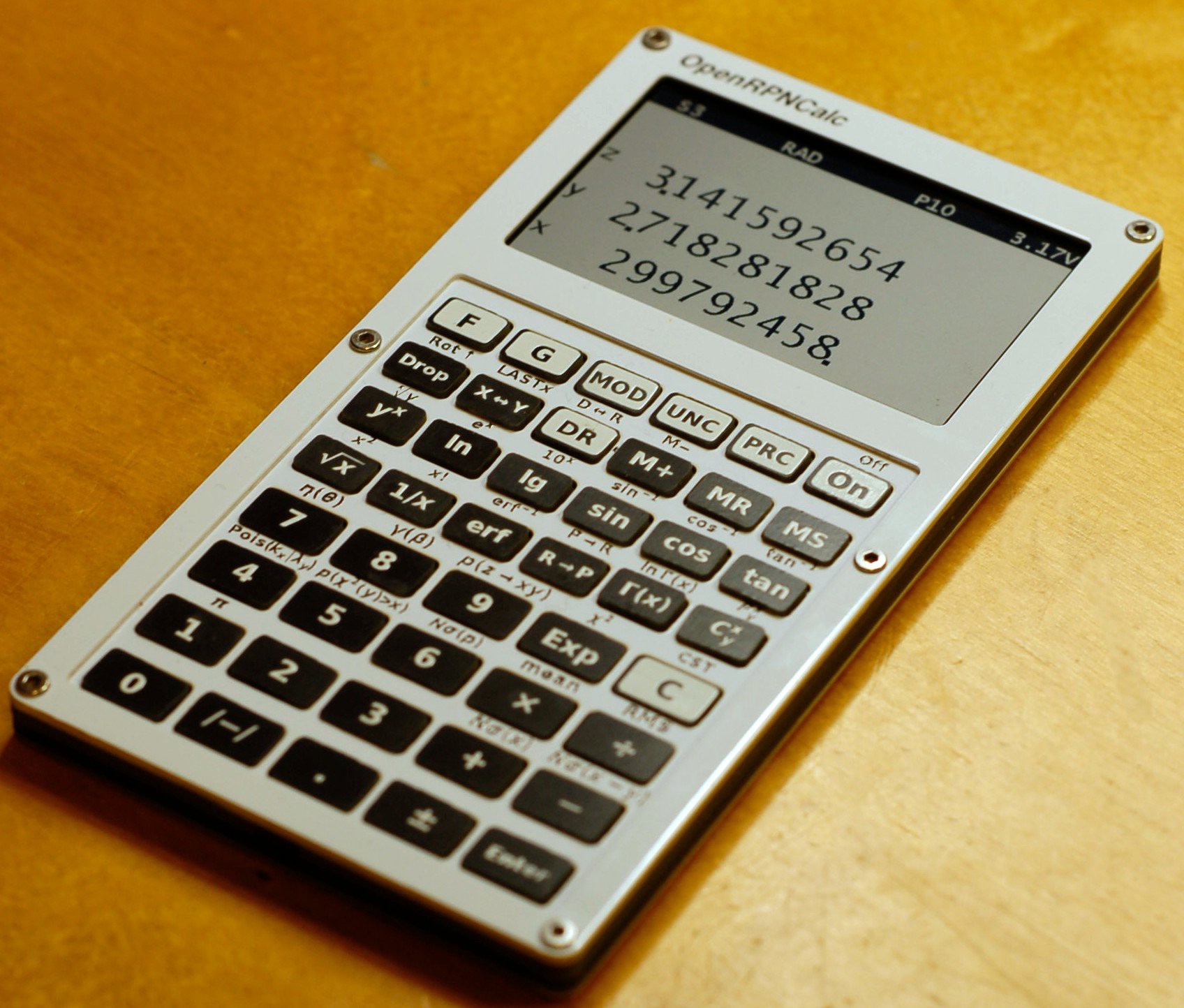
03/05/2025 at 18:15 • 0 commentsTeaser: OpenRPNCalc rev.3 is ready!
![]()
Update in github and logs with the details are coming shortly. -
Online emulator
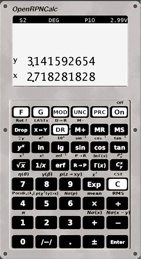
02/20/2025 at 18:42 • 0 commentsIf anyone has wondered how the firmware works, I've made an online emulator using Emscripten, Raylib and the original firmware with a few simple wrappers for LCD and keyboard functions.
![]()
-
Issues to be fixed in the next revision
02/15/2025 at 14:20 • 2 commentsA few (or, in fact, quite a lot) modifications I plan for the next revision of the hardware based on my experience with rev. 2 so far.
Schematics:- External pull-ups. The internal pull-ups in STM32 are around 40 kOhm, which means around 80 uA current draw per single key press (and up to 8*80=0.6 mA if multiple keys are pressed together). This is kind of excessive for the device that draws only ~15 uA most of the time on standby and 1-2 uA when off. For instance, if a few keys get stuck pressed while you carry it in your bag, it will drain the battery in days/weeks. External pull-ups of ~1 MOhm should solve this.
- Power circuit. Currently, power delivery is handled by a pair of Schottky diodes to switch between the battery and external power from ST-LINK when the programming interface is connected. However, even Schottky still drops the battery voltage by 0.2-0.3V. I'll make a simple mechanical switch instead (keeping the Schottky for ST-LINK just in case), which will also allow for a complete power off all the circuitry in case of any interventions like disconnecting the LCD (now I need to take the battery out for that).
- Test pads for debugging to simplify connecting oscilloscope or multimeter to some critical contacts like LCD signals or power rails.
- USART connector just in case?
- I was also considering more modern options for MCU (such as ARM32U5 which seems more power efficient) and 5V booster. Possibly, external switching power (SMPS) for STM32 would also make it more power-efficient, but that needs more investigation - not sure it's the case for the device that lives mostly in the switched-off state.
Casing and keyboard:
- I still want to play with different keyboard designs. The concept with keys made of PCB should work in general, but the keys that are completely floating in the air as they are now are rather wobbly. I plan to experiment with 3D-printed flat springs like I had in the previous design that attach to the keys.
- I know how to make the enclosure even thinner, down to 6.4 mm thickness! More on that when my next batch of PCB arrives from the service. The case will be made completely of a few layers of PCBs, with back lid and front panel based on aluminium core. The back lid will at the same time serve as the PCB for the keyboard switches and the battery holder, and the MCU-LCD part will be connected by a flex cable. Let's see how well it will work.
- The LCD will be upright (in the present design it's placed upside down, which causes some troubles in the firmware related to the text output).
For now, I only have the render of the sandwich of all the PCBs from KiCAD imported to Blender (no LCD 3D model here). With such a tight design, checking everything in the 3D CAD program was essential, hope I haven't missed anything important. More news in a few weeks when the PCBs arrive.
![]()
-
New enclosure design
02/09/2025 at 20:08 • 0 commentsHere are the details about the rest of the enclosure. The case is designed as a sandwich of 3 PCBs (the main board, front panel and the frame holding LCD) and two 3D-printed plastic parts (back lid and spacer between the main board and front panel). All the parts are held together with six 6-mm M2 standoffs and 12 flathead screws.
From bottom to top. Here's the 3D-printed back lid designed in OpenSCAD. You can see a hole for the reset button, an opening on top for the ST-LINK programmer connector, and six slots for standoffs.![]()
Main board (the reverse side opposite to the switches). The change with respect to the first revision is the use of the Keystone 1057 coin battery holder, which sits in the cutout of the PCB and allows the reduction of the thickness of the whole thing. The total thickness of the enclosure is 9 mm compared to 13 mm for the old version.
![]()
A spacer between the main board and the front panel is needed to position the LCD and the keys at the correct distance from the switches.![]()
Front panel PCB with silkscreen labels (0.8mm thickness):
![]()
The frame holding the LCD was originally planned to be made 3D-printed, but I found out that it needs some rigidity, so instead I've made an ad-hoc one from the remaining front panel.Here are a few photos of the guts after soldering. 3D-printed spacer with the front panel attached and key "caps" visible through the holes in the spacer. The LCD is also inserted: the back of it is visible through the battery holder hole, and its flex cable. You can also see the hex standoffs sitting in their holes.
![]()
Same with the main board added on top:![]()
What's that black tape mess, you ask? Unfortunately, it appeared that one of the vias on the PCB had been defective, so the whole column of keys was not working. I had to solder a wire directly to one of the STM32 pins and route it to the opposite side of the PCB. The other four PCBs in my order seemed to be OK (at least, this particular track), but I was too lazy to move the already soldered parts to another PCB given that this revision is anyway not a final one.
Finally, the calculator fully assembled:
![]()
-
New keyboard design
02/01/2025 at 17:43 • 0 commentsSo, the major change in the current design is the keyboard. My aim was to make something that would look not too ugly, last long, could be made relatively cheaply and would be reproducible. I guess PCB silkscreen is the only option that satisfies all that.
My original idea was to make the button of two layers of PCB of different thicknesses, thicker top part (say, 1.6 mm) and thinner bottom (0.8 mm), such that the button would stick over the thin front panel (0.8 mm). I thought it would be a good idea to have the button pivoted to limit its free movement, and for that I planned to use a couple of standard through-hole header pins on the main PCB and matching holes in the bottom button PCB.![]() The plastic part of the pins exactly matches the height of the tactile switches that I used (2.5 mm). Skipping forward, it appeared that the keyboard works better without the pins, but possibly my mistake was that I left too tight a gap between the front panel and the top PCB of the keys (around 0.2mm).
The plastic part of the pins exactly matches the height of the tactile switches that I used (2.5 mm). Skipping forward, it appeared that the keyboard works better without the pins, but possibly my mistake was that I left too tight a gap between the front panel and the top PCB of the keys (around 0.2mm).
The top and bottom PCBs for each key can, of course, be glued together, but a more reliable connection is done by soldering one to another (we have PCBs after all!). For that purpose I left copper pads on the reverse side of the top PCB and tented vias in the bottom part.
I don't think any PCB house would be happy to work with 10x6 mm PCBs, so one has to panelise both key parts. Here's the panelised top PCB:![]()
and its reverse side with copper pads:![]()
and the bottom PCB with tented vias for soldering both parts together and simple holes for "pin suspension":
![]()
I made the PCBs such that they could be soldered precisely before cutting it into pieces, after connecting them with four screws.![]()
However, later I found out that it's in fact much more convenient to cut the board first, and solder the buttons later: cutting the top part of the keys is quite tedious with Dremel since they have a smaller outline than the bottom. One can still solder the cut parts pretty precisely with a simple jig to position them.
Buttons after soldering and cutting:![]()
(the buttons made in the opposite order, cut and then soldered, look much better).
This is the closeup how the buttons look like inserted into the front panel:![]()
As I said, finally I've decided that the pins are not needed, so the through holes in the main PCB are left unoccupied:![]()
That's it for the keyboard part. The rest is coming soon... -
OpenRPNCalc, season 2
01/28/2025 at 18:48 • 0 comments![]()
If you were wondering what happened to this project: yes, it was on hold for a while for various reasons, but now it's back!
The first version of the calculator is still alive, but predictably the stickers have worn out quite quickly, so for revision 2 I decided to try a different approach: the front panel and keys both made of PCB material, with labels printed as a silkscreen. And I think it worked out quite well as a proof of concept, see the photo here.
This version has improvements in both the firmware and (especially) in hardware and enclosure design. I consider it a transitional revision and already see some further improvements to be made for rev. 3. However, I'm going to document this design here anyway, including some pitfalls that I came across.
OpenRPNCalc
Open-source and open-hardware custom scientific RPN calculator
 It's a usual FR4 PCB with a black mask and white silkscreen that would cost you a few bucks in a typical cheap PCB prototyping service. The problem is, my service insists this is a panelised PCB with 44 different designs in it (why not 45, don't they count the frame?) so they ask like 20 times more for this one compared to the other boards of the same size. I agree it's a bit of a stretch to call this a PCB, as it requires a lot of milling and so on, but x20, come on!


 The plastic part of the pins exactly matches the height of the tactile switches that I used (2.5 mm). Skipping forward, it appeared that the keyboard works better without the pins, but possibly my mistake was that I left too tight a gap between the front panel and the top PCB of the keys (around 0.2mm).


