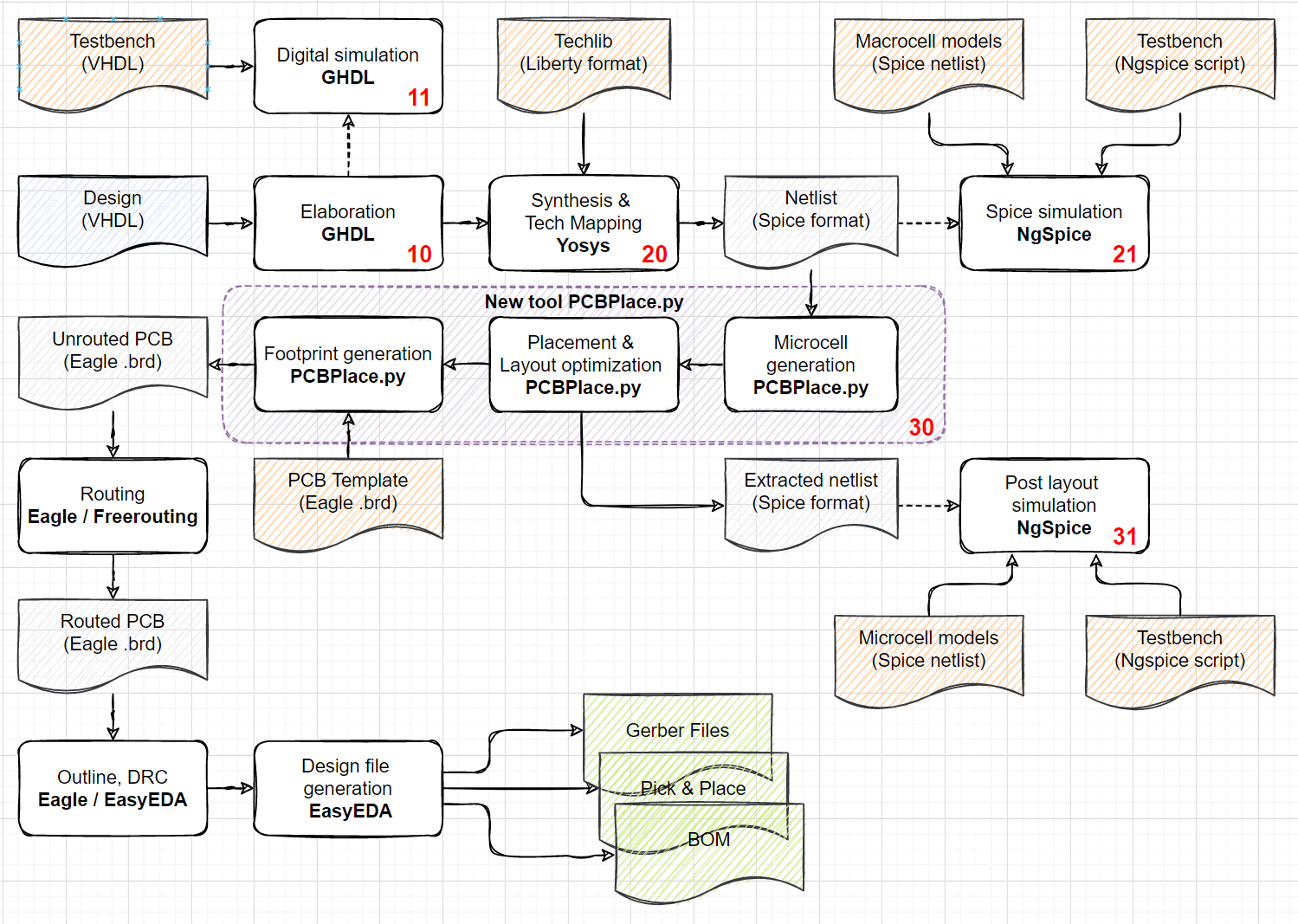
The Flow Architecture

Github repository: https://github.com/cpldcpu/PCBFlow
Work in progress: Flow to synthesize VHDL/Verilog code into a PCB
To make the experience fit your profile, pick a username and tell us what interests you.
We found and based on your interests.
Catching up on an additional round of synthesis test - from last year. I already implemented some changes after observing issues, so this is just an intermediate step.
I combined counter implementation in four different logic families into one board of efficiency.
Next try at analog multiplexer logic: In addition to fixing the bug in the latch, I also added a few optimizations to the logic style: DFF are now taking only 4 amux and I introduced a few additional gate types (ANDN2, ORN2) that helped to reduced logic complexity. As a result, the counter now only takes 21 amux ICs, instead of 26 before. Furthermore, decoupling capacitors are automotically inserted now.
The flow is, of course, not limited to resistor-transistor-logik. In the meantime, I implemented analog multiplexer logic and already received a first PCB with the counter implemented in that logic style. The generated PCB is shown below. The analog multiplexers (BL1551) come in a tiny SC70 package and leave ample space for routing. The implementation of logic gates with multiplexers is quite efficient, hence only 26 devices are needed.
Read more »The fully assembled PCBs arrived a bit quicker than expected. Time for some testing.
Read more »At some point everything has to be put to practice. So, today was time to order some assembled PCBs to check whether the flow actually results in working circuits.
Read more »One issue of the logic style I am using currently is that a D-Flipflop takes up no less than 15 units cells, 15 transistors, 30 resistors. This has a huge impact on design size and it would be great to do something about it.
Months ago, I had a nice discussion with Yann on the TTLer HaD chat and we were competing in trying to reduce the number of transistors in a latch as much as possible. One amazing contraption that came out of this is the design below, that would certainly deserve a more detailed treatment than I can offer here.
After having figuring out where the cells are supposed to go, we need to figure out how to turn them into actual components on a PCB and write them out in a format that can be interpreted by a PCB design tool. As always, I spent most of the time looking for "shortcuts" and only started implementation then.
Finally coming to the tricky part - the placement. The purpose of the placement step is to assign physical locations on the PCB to every unit cell that was generated during synthesis. Cells cannot just be placed randomly, their placement has to be optimized according to various creteria.
Read more »The synthesis step transforms the digital circuit into a spice netlist based on logic cells. To complete the circuit and allow analog simulation we have to actually implement the logic on devices level.
Read more »This is where things get a bit more interesting. I was concerned that it was quite difficult to coerce Yosys into using my custom gate libraries, but in fact it was rather easy.
The "cmos" example proved to be an excellent blueprint to creating a custom library. My logic family of choice is Resistor-Transistor-Logic (RTL), which is based only on resistors and transistors. Coincidentally, this is the same logic family that is used in the famous CDC6600 supercomputer. The basic logic element of RT-Logic is a NOR gate. Hence our design has to be implemented using inverters and NOR gates only. In addition, a storage element, a D-Flipflop, is needed.
Read more »
Create an account to leave a comment. Already have an account? Log In.
Your page https://hackaday.io/project/180839-vhdlverilog-to-discrete-logic-flow/log/200258-3-transistor-latch-7-transistor-dff is gone, was this circuit a failure ?
I accidentally saved it as a draft. The 3T Latch works perfectly.
phew !!! I was worried :-D
One reason to worry is that certain bipolar transistors exhibit avalanche when reverse-biased, sometimes at quite low voltage, like 2V or less, which makes them unsuitable as pass transistors.
I tested old Ge transistors that behave this way, then the behaviour disappeared with more modern Si parts, but the latest RF/microwave transistors might have some reverse breakdown in the "unusable range" again as they trade speed for robustness.
I'm eager to read your report on this story !
Yeah, HF transistors are usually pretty sensitive to higher voltage. Especially Ge ones. Luckily the MMBT3904 is rather robust and appears to work in reverse operation as well, although at lower hfe.
If you can do a DFF (in 7 transistors ?), you can do a shift register and a Johnson counter. From there, you can do ser/des (UART ?) and counting/clockwork.
A clock would be the first thing one does with that technology, right ?
Wow, that looks to me as a very challenging and difficult project. It would definitely be extraordinary if you eventually figure it out !
It turns out that the part VHDL -> spice netlist of RTL logic was actually comparatively easy and doable with Yosys. I have some scripts that do that automatically now.
I have been ponderings for a while about the best approach for place and route - e.g. abuse some of the FPGA tools out there (NextPNR, Verilog to Routing / VTR) or base it on an actual IC flow (OpenLane). Currently it looks like the latter is more accomodating, but the existing opensource tools are really archaic.
Become a member to follow this project and never miss any updates

 Tim
Tim
 Al Williams
 Yann Guidon / YGDES
This is awesome. However, there is something I cannot seem to figure out. How did you convert the splice net-list to a schematic that can be used to generate the routing and 3d board.