Alexander Williams
-
Updated the documentation, check it out
11/27/2021 at 14:43 • 0 commentsI updated the documentation on GitHub, and I think it's worth checking out:
I'm still working on the HOWTO section. I plan to add some diagrams, pictures, and howtos for other topics such as "how to generate Gerbers" and "how to add strain relief". Stay tuned.
-
Add strain relief to RJ45 cables
11/14/2021 at 12:46 • 0 commentsHouston, we have a problem
I've been testing the PCBs from day 1 using a pair of flimsy RJ45 cables. My tests were minimal and leaned towards "does it work" as opposed to "does it work well".
As I upgraded the PCB to v.2 with thicker traces, I also ran my tests with thicker 24AWG RJ45 cables and came to realize the movement is restricted and a lot of pressure is applied to the connectors as the printhead moves around the XY axis'.
A simple solution
I know this might seem obvious to some, but some minimal/basic strain relief should be added to the RJ45 cables, with a ziptie or velcro wrap. I made a simple loop with both cables and then tied the loop.
This prevents the RJ45 cables from moving around too much in the connectors, while still maintaining the ability for the printhead to move around freely.
Something like this should work as well:
![]()
-
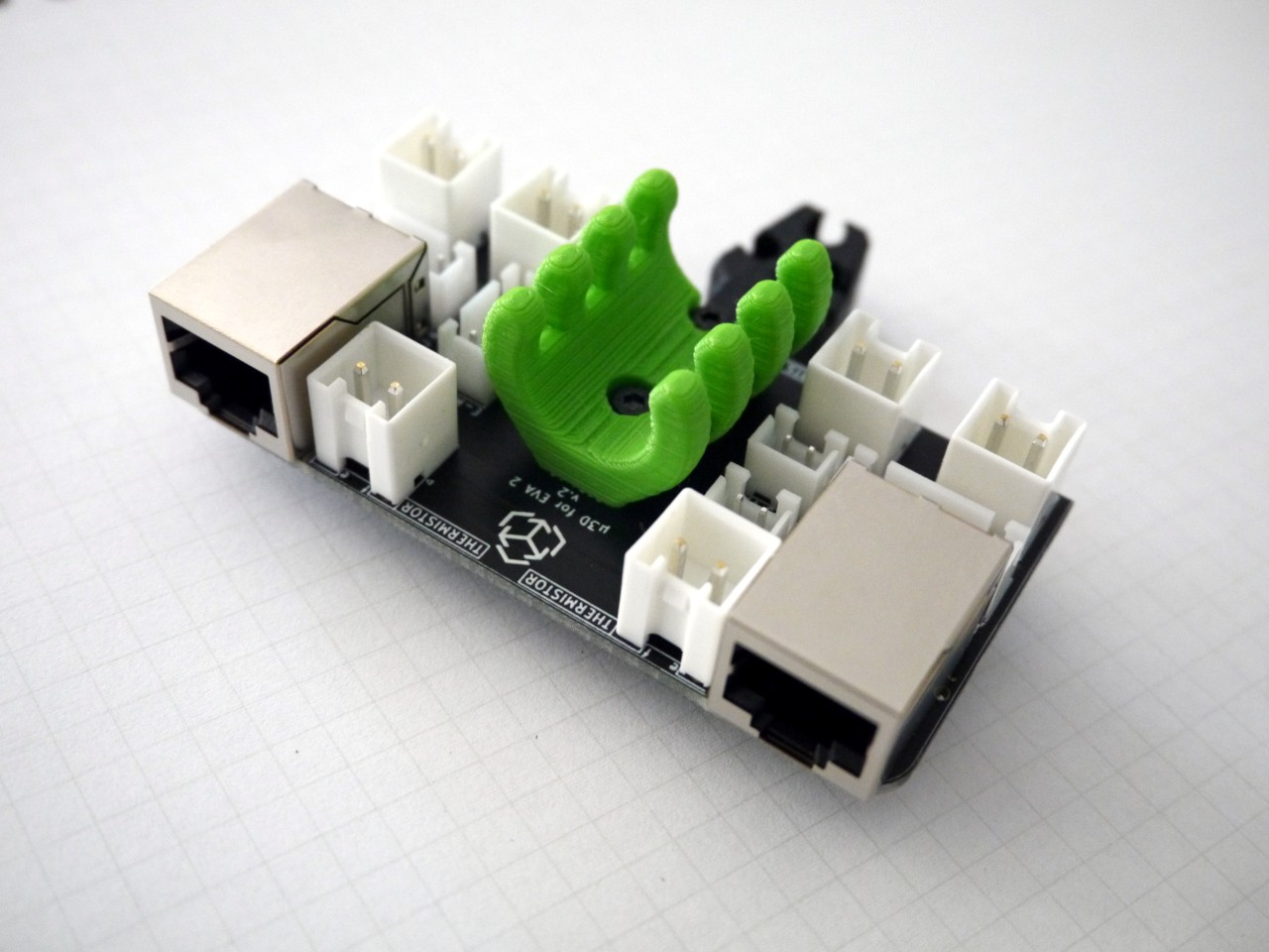
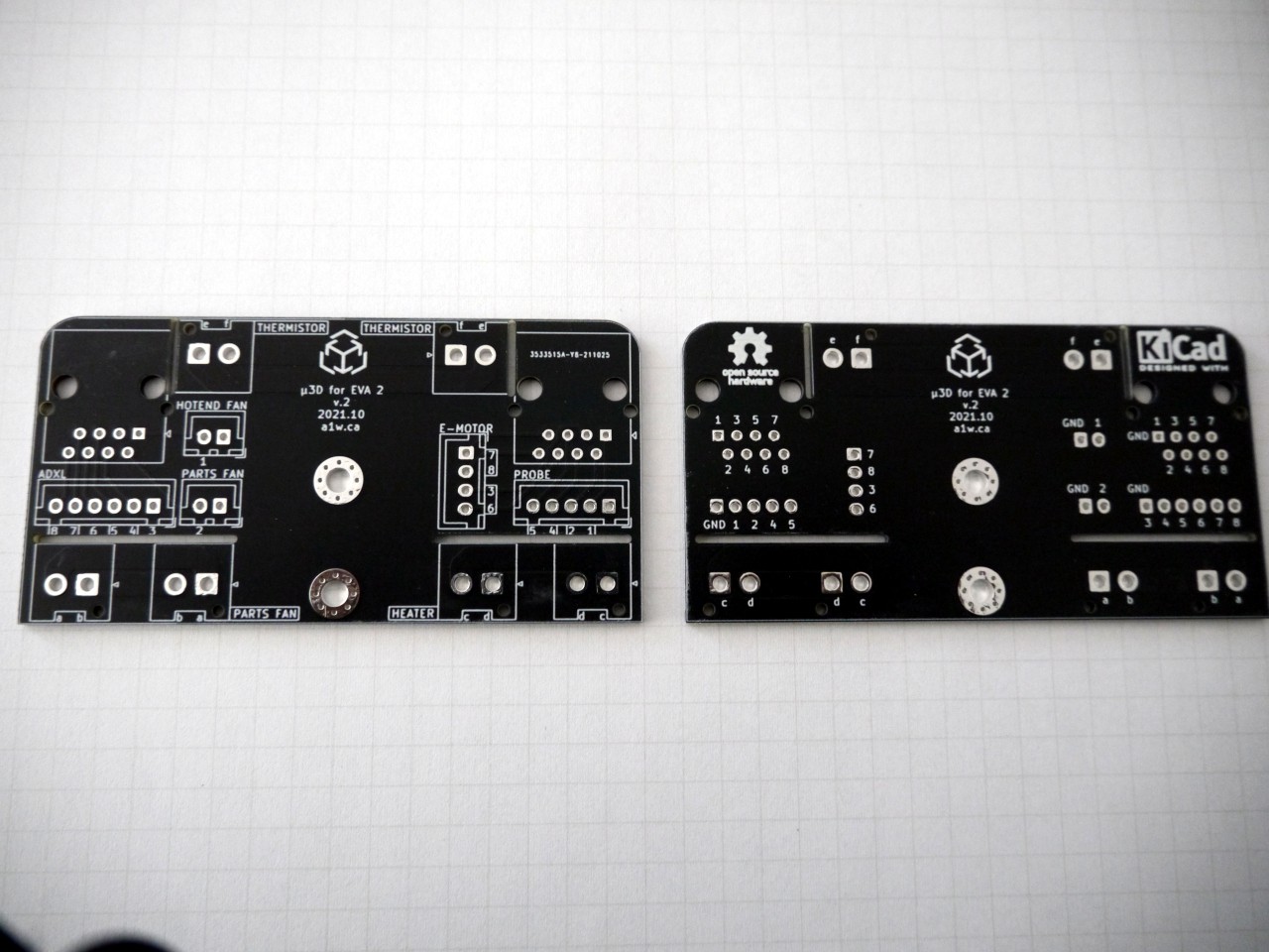
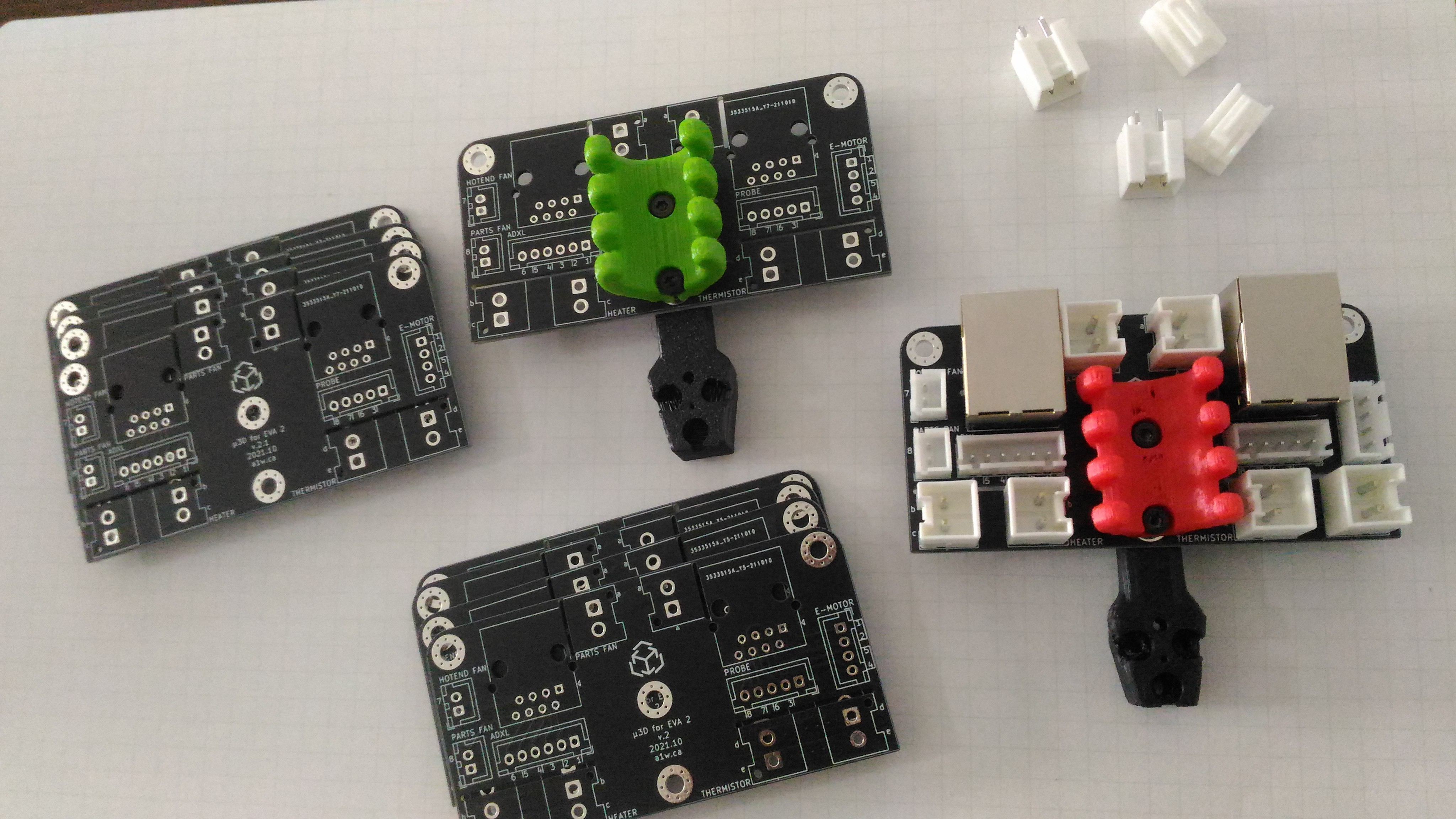
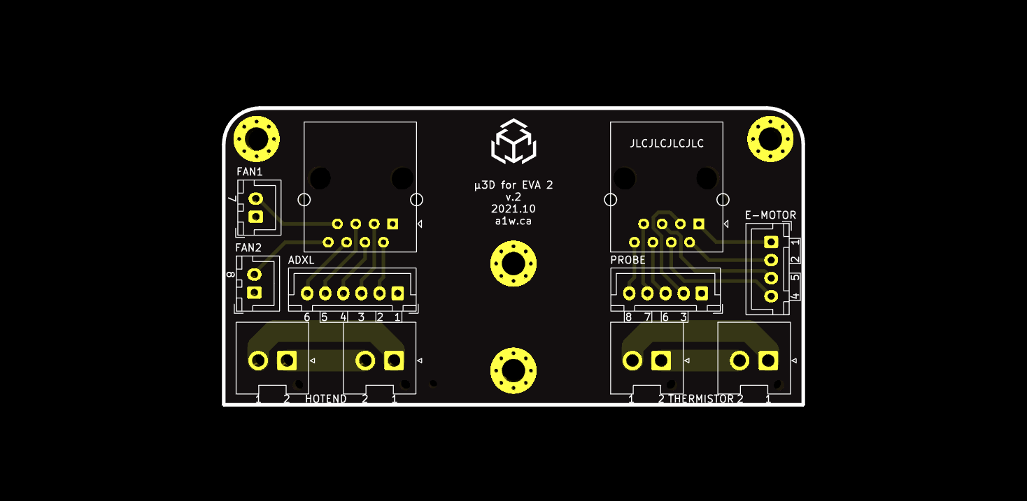
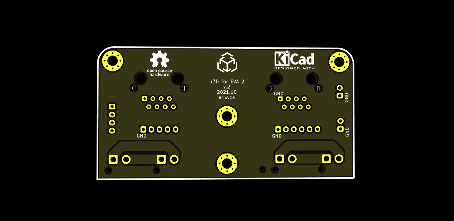
Received the v.2 PCBs today!
11/11/2021 at 06:24 • 0 commentsI've finally received the v.2 PCBs today, did some tests and can confirm they are acceptable.
![]()
I did notice one minor mistake: pin 1 on the RJ45 below the KiCad logo is marked as GND but GND is actually pin 3. It can be quickly confirmed with an electrical continuity test.
![]()
Despite the silkscreen error, everything works fine and the high current traces are tested up to 2A, even though the theoretical limit is much higher.
I am updating the documentation today and will publish v.2 for sale on Tindie hopefully by tomorrow.
![]()
-
Ordered PCBs for v.2
10/25/2021 at 11:41 • 0 commentsI've made a production order for v.2 PCBs. They'll be available for purchase on Tindie as soon as I receive them.
The thermal tests are mostly complete. Essentially I wanted to confirm if the 3mm PCB traces can handle a 50W hotend heater: they can with no temperature increase @ 2A/24V.
Based on some calculations, with a conservative 5deg C temperature rise, one trace should handle at most 3.9A but since I doubled the traces on both sides of the PCB, it could handle possibly 7.8A, however that's extremely theoretical and I would caution against more than 5A. I haven't tested with that much current so it's at your own risk.
Moreover, it's probably a good idea to fuse the cables to be extra safe.
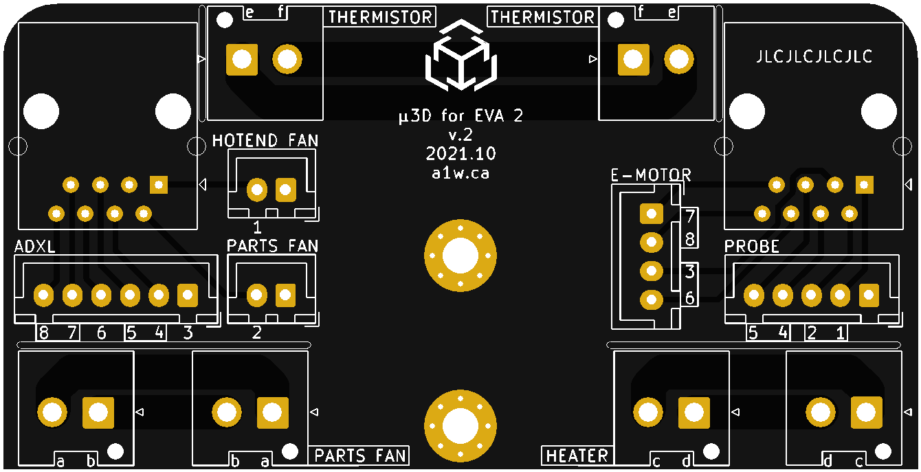
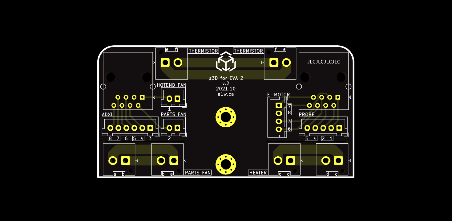
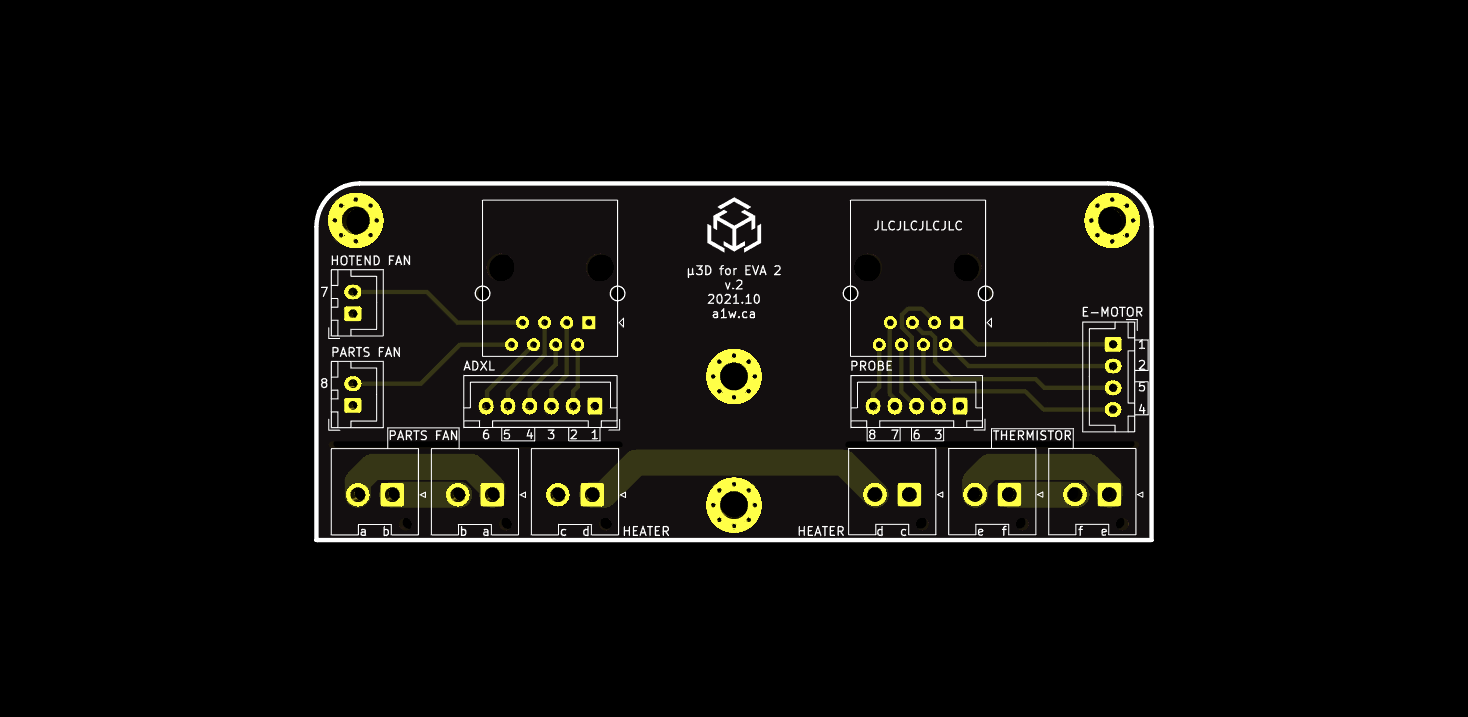
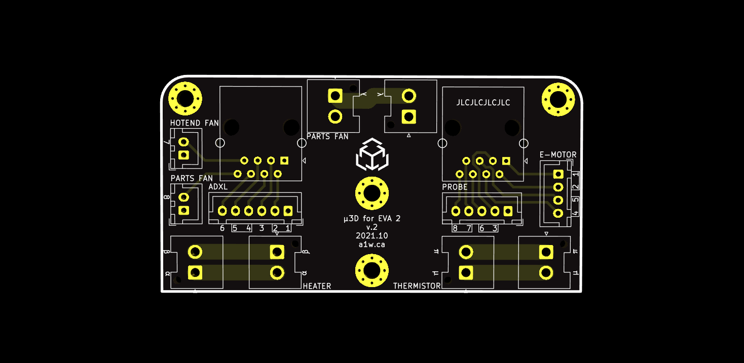
Here's a view of the final front and back of the PCB:
![]()
![]()
A few things to note:
- I labeled the high-current pins with letters instead of numbers, since they don't map to the RJ45 numbered pins. With this information, it should be quite obvious how to correctly crimp the JST-VH cable assemblies.
- I added some openings to separate the high-current connectors from the low-current connectors, as a way to isolate the signals and provide a way for heat to escape (probably overkill haha).
- On the front of the PCB, I labeled where I think the thermistor, parts fan, and heater should be wired, but those are completely optional.
- The JST-VH connectors do not share GND, which provides additional wiring and voltage flexibility (ex: a 5V parts fan can be used and powered by a totally separate 5V power supply).
- There are actually two (2) connectors labeled "PARTS FAN", that's to allow for either 1) wiring a 3-pin or 4-pin fan (ex: GND, PWR, PWM, SPEED) or 2) wiring a third non-PWM (2-pin) fan or other device. If a PWM fan is used, I recommend wiring GND and PWR through the high-current connectors (even if it's a low-current fan), and using pin 2 on the JST-XH for the PWM signal (and not wiring the GND on the JST-XH connector).
Stay tuned for the next update within a week or two.
-
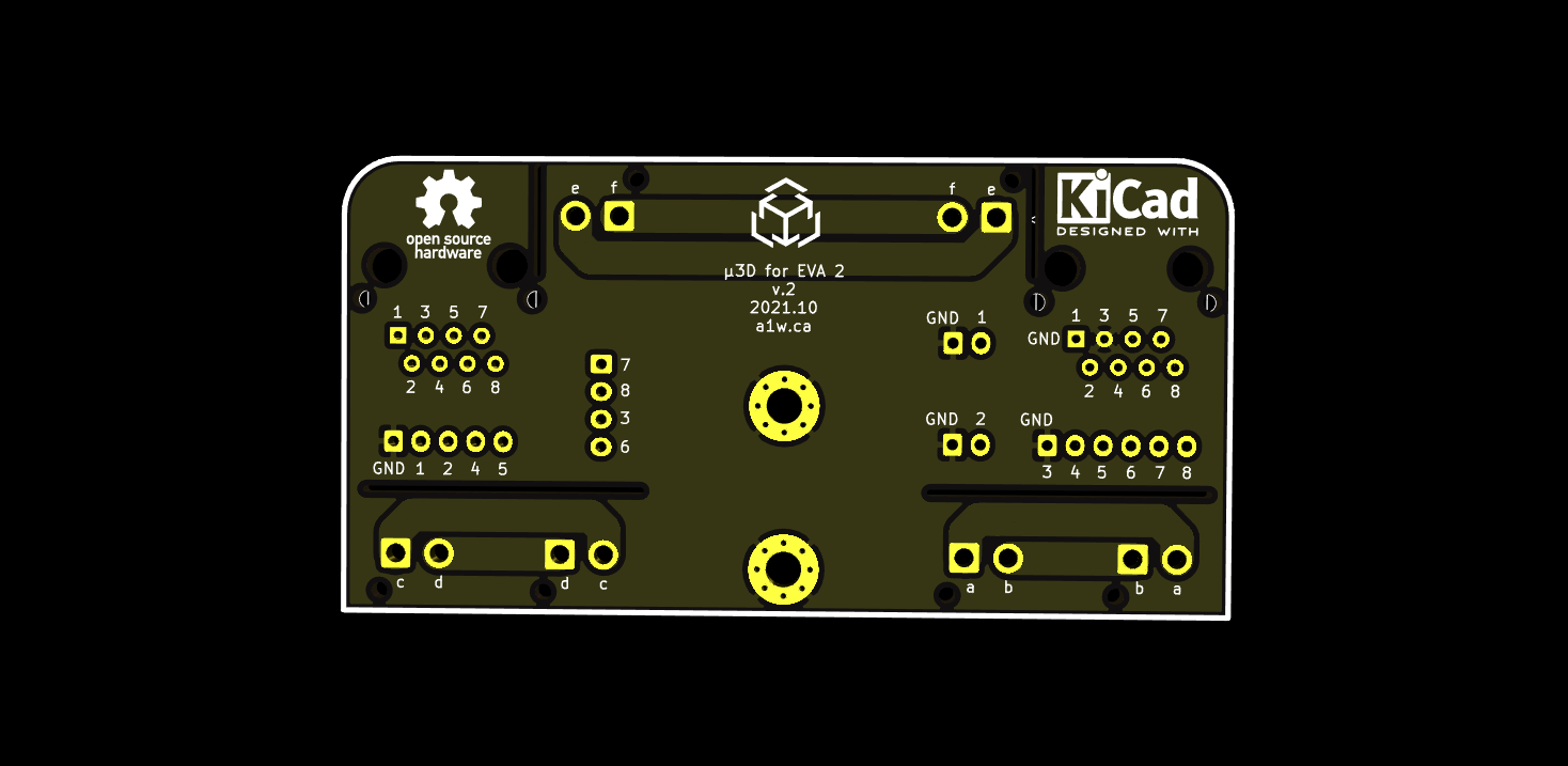
Back to 80mm
10/24/2021 at 13:40 • 0 commentsIn the previous log entry, I mentioned extending the board from 80mm to 96mm. To be honest, I hated that idea because it's just too long and didn't look very nice.
After some messing around in KiCad, I decided to bring the width back down to the original 80mm.
![]()
I moved two JST-VH connectors back up top and moved the RJ-45 connectors towards the edges of the PCB. I also removed two of the M3 mounting holes because they weren't really necessary.
This design tucks the smaller JST-XH connectors between the larger JST-VH connectors, but there should be enough spacing for them to still be accessible once cables are connected.
The one unfortunate downside of this design is I had to reroute all the existing traces. Now the RJ45 pin assignments are completely different for every connector, however it might only be necessary to re-do the wiring assembly for the ADXL: it's the only connector whose pairs don't lineup like the v.1 PCB (comparing v1 and v2 boards will make that very clear). The other connector/wiring assemblies should work just fine without changes, unless you're doing something esoteric then it's probably best to follow the new pin assignments.
Anyways, I'm quite satisfied with this design so far. All the issues from the previous v.2 batch are fixed without altering the dimensions of the board.
This week I'll perform some thermal tests on the 3mm traces for the latest PCBs. Depending on those results, I hope to ship this v.2 board to production by mid-week.
-
Received the PCBs today, and an improved design
10/24/2021 at 03:47 • 0 commentsI received the v.2 PCBs but I'm not very impressed.
![]()
I haven't soldered the components, but you can see I made a few minor PCB design mistakes:- the new JST-VH connectors are facing the cable holder. This makes it quite difficult to disconnect the cables.
- The new JST-VH connectors at the top of the PCB are blocking the wires from the cable holder, which will prevent wiring of cables through the holder.
These issues may seem trivial, but I want a better experience with using the PCB. For that reason I've redesigned the PCB once more by extending the width from 80mm to 96mm. It adds 8mm to each side, which allowed me to add all 6 JST-VH connectors to the bottom of the PCB. I think it isn't too bad. Hopefully it won't make the printer head unbalanced.
![]()
It has 3mm traces on the front and back of the PCB. I'll need to think about this for a bit more. I'm still not sure if this will be the final v.2 design.
-
Ordered v.2 PCBs but not for production
10/09/2021 at 14:22 • 0 commentsI received a bunch of 3.96mm JST-VH connectors, and they are awesome! They're much larger than the JST-XH connectors, so their 10A rating definitely inspires confidence.
However i'm still unsure about the PCB. I want to perform some thermal tests on different types of high current traces with the boards from this specific manufacturer (JLCPCB), so I ordered a handful of PCBs with slightly different trace designs for the hotend heater and thermistor.
I'll run my tests and report my findings once the v.2 PCBs arrive (within the next 2 weeks).
-
Updated v.2: Fans, Hotend and Thermistor wiring!
10/06/2021 at 05:28 • 0 commentsIn the previous log entry, I mentioned that I added support for wiring the hotend heater and thermistor.
This time, I also added two (2) more JST-VH connectors at the top of the PCB, for a high-current parts fan (aka layer fan). For each connector, one pin is GND and the other is PWR.
![]()
This is cool because it automatically adds support for a hardware PWM fan as well (3 wires), which is typically a useful feature for parts fans. To use a PWM fan, you simply need to wire the PWM signal to PIN 8 on the left "Parts Fan JST-XH" connector, and then PWR/GND on the middle "Parts Fan JST-VH" connectors.
Alternatively, it can also be used to wire a third fan, where each FAN connector only supports PWR+GND without a PWM signal.
I've also changed the orientation of the lower JST-VH connectors to allow for nicer/straight traces, and I changed the labels on the pins to avoid confusion with the RJ45 pins.
Overall I kind of like this design since it's much more flexible and provides various different wiring options for lots of components.
-
Updated v.2: Hotend and Thermistor wiring!
10/05/2021 at 14:19 • 0 commentsI guess it was inevitable, but after much feedback on the RatRig Discord, I've decided to update this PCB design to support hotend and thermistor wiring.
![]()
![]()
The PCB is now 80mm x 41mm instead of 80mm x 30mm. The extra height adds space for four (4) JST-VH connectors, which have 3.96mm pin spacing instead of typical 2.54mm. They can also support up to 10A when using 16AWG wires.
The hotend and thermistor each have 2 connectors per PCB, rather than wiring through an RJ45 cable (too thin). One connector goes to the heater cartridge, the other would go directly to the 3D printer control board, or to the corresponding JST-VH connector on the other PCB. The connectors are essentially acting as a passthru for a quick-swap hotend assembly.
There are 3mm traces between pins 1 and pins 2. I chose 3mm to somewhat match the through-hole pad size of 2.7mm. The traces themselves can support up to 3.9A with a 5deg C temperature rise, or 7.2A with a 20deg C temperature rise. For that reason, I went a bit overboard and added identical 3mm traces on the front AND back of the PCB, so theoretically they should support double the current (7.8A to 14.4A). That idea may be flawed, so I'm not sure if it'll end up in the final v.2 board.
The 50W E3D V6 has a maximum current draw of 3.9A@12V, 2.8A@24V.
The 80W E3D SuperVolcano has a maximum current draw of 8A@12V, 3.9A@24V.
With all that being said, this setup should technically support even the craziest/power hungry hotends, but I wouldn't recommend it without proper testing and careful monitoring.
I'll sleep on this design for a bit before submitting it to the fab.
Note for owners of v.1: I'll be happy to send a free pair of v.2 PCBs to those who've already ordered v.1 PCBs. You'll only need to pay for shipping (and maybe import taxes/VAT... sigh).
μ3D: RatRig V-Core 3 EVA wiring over RJ45
A daughter board that mounts on a 3D printer hotend assembly to enable all wiring over RJ45