 Ken Yap
-
Version 1 putting the modules together
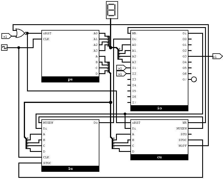
08/23/2021 at 09:54 • 0 commentsFirst I had to correct errors in the modules. Then I needed a NOR gate to combine the reset button with the NOPF reset signal. In addition I have attached a clock generator, a hex instruction address display, input and output pins for the test program, and a LED on output 7.
![]()
The program simulated was the one used in the Arduino emulator:
LD 1; AND 2; STO 3; STOC 7; NOPF;
and letting the simulation free-run showed it looping through the instructions, and lighting the LED if I1 AND I2 is FALSE; STOC 7 effectively makes the LED show a NAND.
I'll test it a bit more before posting the Logisim files, and decide what the next stage, if any, should be.
-
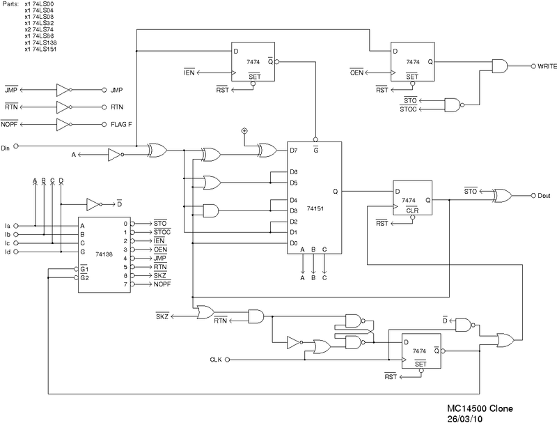
Version 1 preparing to put the modules together
08/18/2021 at 04:06 • 0 commentsI'm going to split this into two logs. At first I thought I could write one log with the modules connected together and the results of testing, but it turns out that I have to go back and fix various infelicities in the modules due to my learning to use Logisim. As I don't want to continually revise logs like some authors do, making it difficult for readers to see what's changed, I will describe the preparation now. I also have to go back and rewrite history, er module logs, to fix up the sub-circuits.
I need to label all the external connections of each module, not with text but with pin labels, otherwise you cannot see from outside each pin's function. Also the pin label field has the hint HDL compatible on a yellow background. What this means is only certain characters are valid. I cannot use ~ or / to indicate inverted logic, so I have to write it like nRST.
To combine modules, the Merge action is used. However this reads in the module once rather than linking to it. So if the module changes, the sub-circuit has to be deleted and reread. When merging, module names need to be unique, or existing modules will be overwritten. So instead of letting the module name default to main I gave each one a unique name.
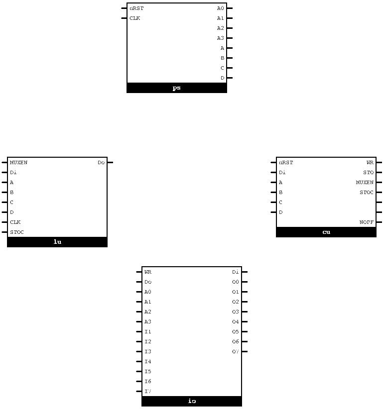
So for now here are the 4 modules read into one project:
![]()
-
Version 1 Logisim of Input Output
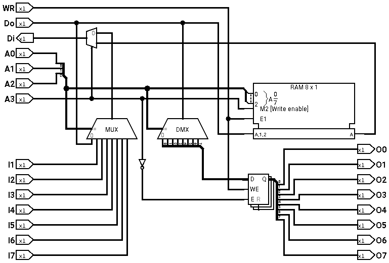
08/12/2021 at 01:19 • 0 commentsThere are 16 locations addressed by the address nybble of the 8-bit code word. We allocate the bottom 8 locations to I/O, and the top 8 locations to scratchpad memory which is used for temporary booleans. Input 0 is special, it's the Result Register. Being able to read back the RR is required for most configurations. Here is the Logisim circuit:
![]()
As expected, A3 is used to disambiguate between I/O and scratchpad locations.
A couple of notes: The demultiplexer and output register could be combined in one chip so the 8-bit bus between the two is intrachip. The 2 to 1 selector between the multiplexer and the RAM could be dispensed with if both of them support tristate outputs switched by A3 of course. Both these points highlight that often Logisim doesn't have the parts that exist in the real world, although they can be synthesised by existing gates. Or one could write a Java implementation of a chip, but that is more work. We shall return to this point.
-
Version 1 Logisim of Program Store
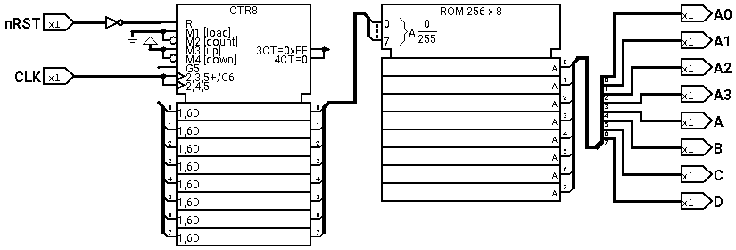
08/09/2021 at 00:22 • 0 commentsRecall that the MC14500B does not have a program counter so it has to be implemented external to the chip. So the program store is straightforward, an 8-bit counter coupled to an 8-bit wide ROM.
![]()
The counter in Logisim has many features but we use only some of them.
The high nybble of the code byte is the operation and the low nybble is the address of the port or scratchpad memory.
-
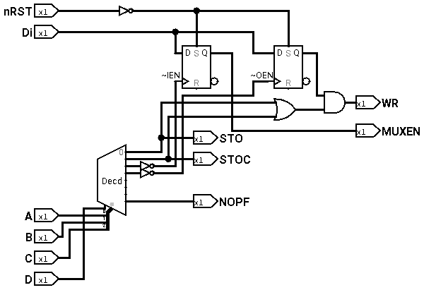
Version 1 Logisim of Control Unit
08/07/2021 at 12:31 • 0 commentsNow we complete the instruction processing by dealing with the upper 8 instructions, the ones that have the high bit on, comprising STO, STOC, IEN, OEN, JMP, RTN, SKPZ, and NOPF. In this version we don't implement JMP, RTN and SKPZ. Here is the Logisim design for the rest.
![]()
We use a 3 to 8 decoder/demultiplexer to enable one of 8 outputs when that particular instruction is selected. The D line is used to enable decoding for this group of 8. Unlike the TTL design I'm following, I intend to use an active high out decoder, the 74LS259, instead of the original active low out 74LS138. So the Write line is enabled using an OR gate whenever STO or STOC is executed. STO or STOC are also used in the Logic Unit to invert Do.
IEN and OEN are inverted and used to clock in the input data. The inversion means that the Di is clocked in at the falling edge of the IEN or OEN lines depending, meaning at the beginning of the next instruction. I was uncomfortable with using IEN and OEN to clock the D flip-flops this way but this is in fact how it's represented in the block diagram of the innards of the MC14500B. Note that the flip-flops are reset to IEN and OEN high with nRST.
Commentary on more use of Logisim: It's fairly easy to verify combinatorial circuit behaviour, but sequential circuits take more effort, because of the extra dimension of time obviously. It would be nice to have models for various TTL chips, but only a handful are supplied in the standard package. So the generic parts such as decoder, D flip-flop, etc. may differ from the actual part you hope to use. For example, in the diagram above the R and S lines of the flip-flops are active high but in the actual design, they will be active low. Hence the inverter for the nRST line.
-
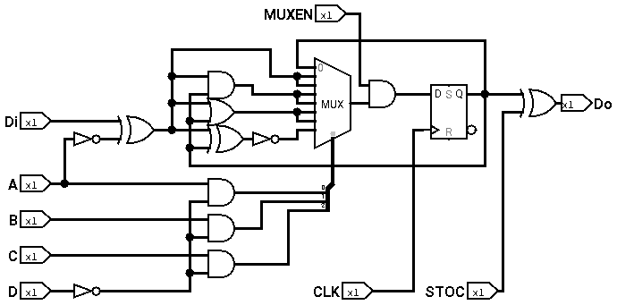
Version 1 Logisim of Logical Unit
08/05/2021 at 10:52 • 0 commentsFirst thing is to see what has been done before. In the project #One Bit CPUs a previous design in TTL is mentioned and the diagram is here.
It makes sense to elaborate the design modularly, so let's first look at instruction processing. You'll notice that the 16 instructions fall into two groups when you exclude the NOPs at 0 and F. The first 7 are load and logical operations. while the next 7 are store and control operations. The difference is that only the former affect the result register (RR). So I'll adopt the design and create a logic unit LU (no arithmetic, so not ALU). This is done using gates and an 8 input multiplexer feeding a D flip-flop which is the RR.
![]()
In order from 0, the operations are NOPO, LD, LDC, AND, ANDC, OR, ORC and XNOR. The first is just the identity transform, so RR out is looped back to RR in. At this point I have to gripe about the ordering of the operations as designed. LD is 1 and LDC is 2. It would have been nice if XNOR had been moved to 1, then LD and LDC would be 2 and 3 respectively, thus differing in only one bit. Similarly for AND and OR. Fortunately this doesn't complicate the circuit because of the multiplexer, we just use A to invert the Di as necessary.
The instruction line D is used to force the operation to NOPO using 3 AND gates so that the RR is unchanged by the top 8 instructions. In the original design this was done by futzing with the clock signal. I believe this is a mistake because it can lead to glitches.
If you have been following the project, you may notice that the circuit has been updated to be modular, see this log.
-
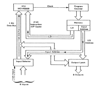
Version 1 emulator
08/01/2021 at 02:10 • 3 commentsThis is the block diagram of the system that is emulated. Not shown are the scratchpad locations for memory, and the FLGF reset line, see description below.
![]()
It was relatively easy to write an emulator for the Arduino.
/*
        MC14500B Industrial Control Unit system emulator Version 1
*/

#define DEBUG
#define HALFPERIOD  100 // sets speed of emulation

// All 16 instructions
#define NOPO  0x0
#define LD    0x1
#define LDC   0x2
#define AND   0x3
#define ANDC  0x4
#define OR    0x5
#define ORC   0x6
#define XNOR  0x7
#define STO   0x8
#define STOC  0x9
#define IEN   0xA
#define OEN   0xB
#define JMP   0xC
#define RTN   0xD
#define SKPZ  0xE
#define NOPF  0xF

struct icu {
  byte  counter;        // current instruction
  byte  clock;          // code executed on low phase
  byte  rr;                 // access to I/O address 0 goes here
  byte  flg0;
  byte  flgf;
  byte  ien;
  byte  oen;
  byte  jmp;
  byte  rtn;
  byte  skpz;
} icu;

const byte code[256] = {
#include "code.h"
};
byte rwmem[8];
const byte iportmap[8] = { 0, 2, 3, 4, 5, 6, 7, 8 };
const byte oportmap[8] = { A0, A1, A2, A3, A4, A5, 9, 13 /*LED*/ };

byte read(byte addr) {
  if (icu.ien == 0)
    return 0;
  byte port = addr & 0x7;
  return addr & 0x8 ? rwmem[port] : (port == 0 ? icu.rr : digitalRead(iportmap[port]));
}

void write(byte addr, byte data) {
  if (icu.oen == 0)
    return;
  byte port = addr & 0x7;
  if (addr & 0x8)
    rwmem[port] = data;
  else
    digitalWrite(oportmap[port], data);
}

void setup() {
  // put your setup code here, to run once:
#ifdef DEBUG
  Serial.begin(115200);
#endif
  memset(&icu, 0, sizeof(icu));
  icu.ien = icu.oen = 1;
  for (byte i = 1; i < sizeof(iportmap) / sizeof(iportmap[0]); i++)
    pinMode(iportmap[i], INPUT_PULLUP);   // means unconnected pins will be 1
  for (byte i = 1; i < sizeof(oportmap) / sizeof(oportmap[0]); i++)
    pinMode(oportmap[i], OUTPUT);
}

void loop() {
  // put your main code here, to run repeatedly:
  for (icu.counter = 0; ; icu.counter++) {

    icu.clock = 1;              // high phase, fetch
    byte c = code[icu.counter];
    byte instr = c >> 4;
    byte addr = c & 0xF;

#ifdef DEBUG
    Serial.print(icu.counter, HEX);
    Serial.print(" ");
    Serial.print(c, HEX);
    Serial.print(" ");
    Serial.println(icu.rr, HEX);
#endif

    delay(HALFPERIOD);

    icu.clock = 0;              // low phase, execute

    // on flgf jump to beginning of program
    if (icu.flgf) {
      icu.flgf = 0;
      icu.counter = 255;
      continue;
    }
    icu.flg0 = icu.flgf = 0;    // reset flags

    // todo: deal with jmp and rtn
    if (icu.skpz) {             // skip instruction
      icu.skpz = 0;
      continue;
    }

    icu.jmp = icu.rtn = icu.skpz = 0;   // reset control flags

    switch (instr) {
      case NOPO:
        icu.flg0 = 1;           // currently no-op
        break;
      case LD:
        icu.rr = read(addr);
        break;
      case LDC:
        icu.rr = !read(addr);
        break;
      case AND:
        icu.rr &= read(addr);
        break;
      case ANDC:
        icu.rr &= !read(addr);
        break;
      case OR:
        icu.rr |= read(addr);
        break;
      case ORC:
        icu.rr |= !read(addr);
        break;
      case XNOR:
        icu.rr ^= !read(addr);
        break;
      case STO:
        write(addr, icu.rr);
        break;
      case STOC:
        write(addr, !icu.rr);
        break;
      case IEN:
        icu.ien = icu.rr;
        break;
      case OEN:
        icu.oen = icu.rr;
        break;
      case JMP:
        icu.jmp = 1;
        break;
      case RTN:
        icu.rtn = 1;
        break;
      case SKPZ:
        icu.skpz = 1;
        break;
      case NOPF:
        icu.flgf = 1;
        break;
    }
    delay(HALFPERIOD);
  }
}
And the first test program is:
// Test program: LD 1; AND 2; STO 3; STOC 7; NOPF;
// Input pins are pulled high by default so
// grounding either pin D2 or D3 should turn on LED
0x11, 0x32, 0x83, 0x97, 0xF0
Relevant points about this design
The program storage (PS) is 256 bytes so the program counter is 8 bits wide. Each instruction and operand fits in a byte, the 4 MSBs are the instruction and the 4 LSBs are the address. As mentioned before, the program counter is not on-chip, it has to be provided externally. It is incremented by the clock signal. In the high phase, the code nybble is read in and in the low phase, it is executed, making use of the address nybble if necessary. The clock variable is only written to and never read so it's redundant, but I find it useful to use this as documentation to read the timing diagrams in the handbook.
(An interesting diversion is to ask whether this is a small endian or big endian design. In this design both nybbles are read in one go, so it has no endianess. But in the case of 4-bit wide PS where the code nybbles are interleaved with the address nybbles, using the clock as the LSB, you can see that since the code is read when clock == 1, this means the address nybble precedes the code nybble so it's little endian.)
4 bits for the address means we can potentially address 16 input ports and 16 output ports, distinguished by the write line. The top 8 addresses are directed to RW memory, so we have only 8 each of input and output ports. In addition, on the Arduino, output port 7 is directed to the builtin LED so that we can control it from a program.
Execution starts at program byte 0 and wraps around after 255. So in the simplest design, all of the PS is executed repeatedly. How do we make sure that trailing bytes after the desired code don't do anything untoward? There are two ways:
Firstly the codes 0x0 (NOPO) and 0xF (NOPF) are both no-ops, the reason being that the blank state of PROMs in that era were either all 1's or all 0's. But note that this doesn't change the cycle length, it just executes no-ops until the counter wraps around. This is when execution speed is not critical.
The second way is to use the fact that NOPO and NOPF generate a pulse at the respective pin when executed. In this design we use the NOPF pulse to reset the counter to 0, thus jumping to the beginning of the program. This will shorten the cycle length.
The IEN and OEN instructions are used to disable input and output for sections of code. This method of conditional execution also doesn't change the cycle length. We haven't implemented JMP, nor RTN and SKPZ. These require extra hardware. For example JMP implies external hardware to load the program counter from the address. And the address would have to be wider to cover the PS space. Not for this version.