-
Draft Prototype Shield Schematic
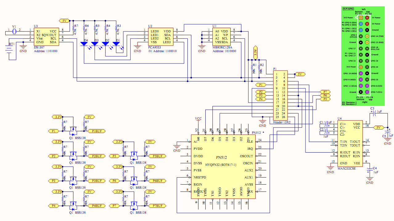
07/26/2014 at 07:06 • 0 commentsHere is a draft shield schematic:
![]()
Each of the I2C devices work with 3.3V (DS1307 is 5V, but the I2C bus is open collector and it supports 3.3V comms) so there is no level shifting required here.
The PN512 won't be on the prototype board here since it is located on the NFC Explore, but it is here to map out used pins. In the final version, it will be completely integrated with the shield. Note that the pins not required by the NFC Explore board will only go to the prototype board underneath and will be trimmed (the NFC board will sit on top).The extra GPIO pins here are buffered using the well known BSS138 to 5V. The 5V value for individual I/O can be swapped for any other voltage as requred. This also provides protection to the pins.
More to come tomorrow.
-
Explore NFC Layout
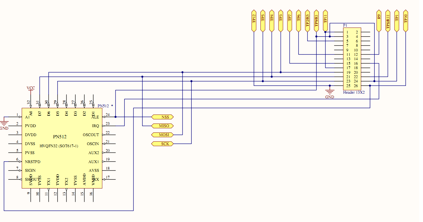
07/19/2014 at 06:16 • 0 commentsHere is the traced out SPI/comms configuration for the NXP Explore NFC RasPi board:
![]()
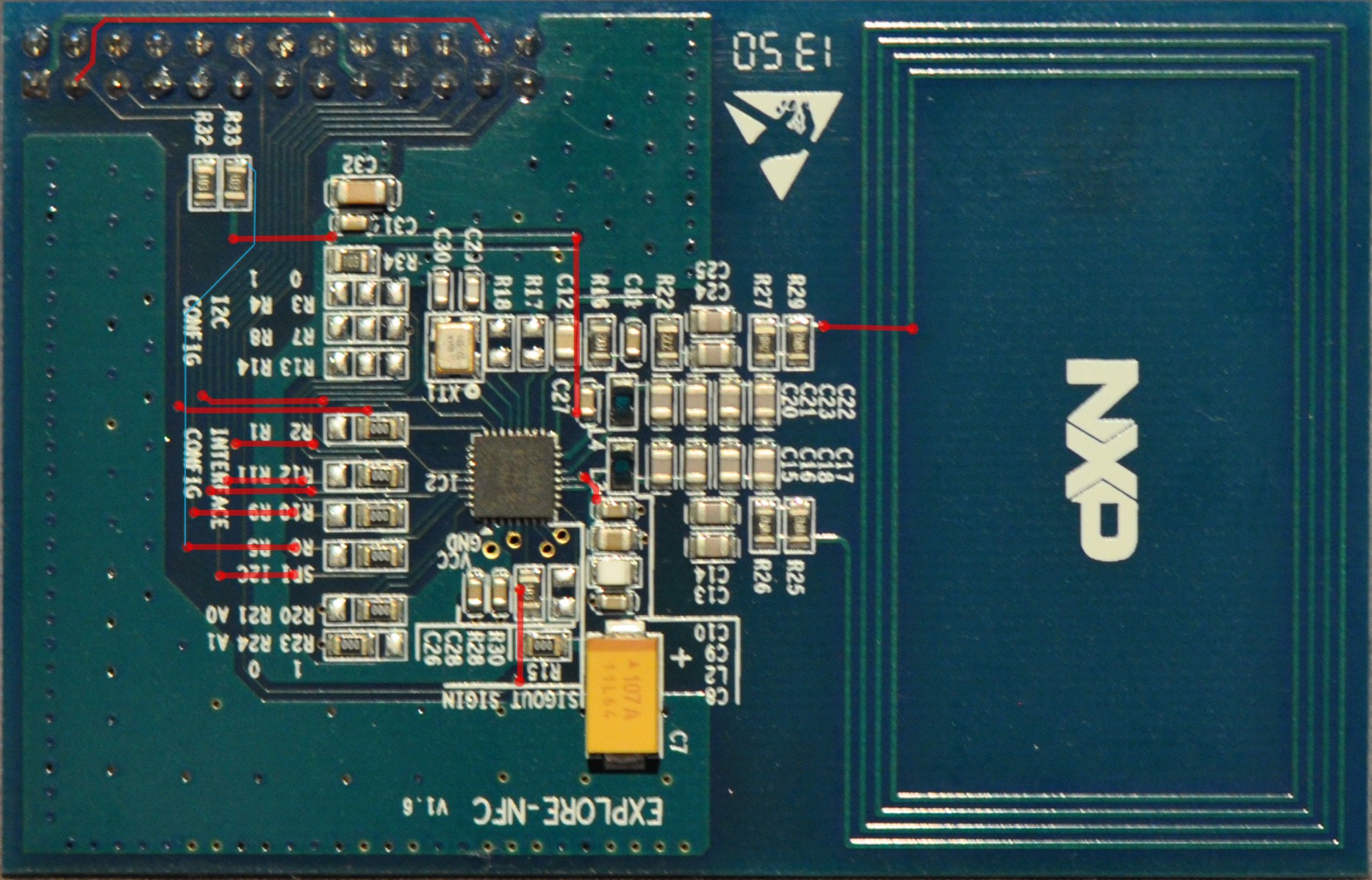
On the board are 0-ohm resistor links to reconfigure as I2C. I have marked where appropriate, the connection pads for these. The header here corresponds to the this image. The TP designations are test points located on the bottom of the board.
When reconfiguring, you will need to move the resistor links. Here is the board layout when configured for SPI:
![]()
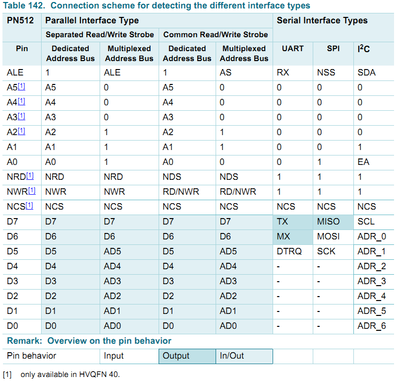
When reconfiguring, be mindful that the PN512 auto detects the serial connection based on the configurations from the table below (taken from the datasheet):
![]()
So what was the issue I posted in the previous log. Well notice that pin 3 and pin 24 are connected together. Pin 3 in this instance is used for NSS (!Slave Select) from the SPI comms (as per the software library too). If we are to use I2C for other things (using the default pins on the RasPi for this) we would need to remove pin 3 from this board (pin 5 while connected, doesn't connect to anything except a bare pad. We could remove this too to reduce noise.
Because I will be using an intermediate dev board layered between the NXP board and the RasPi for the prototype circuit, I can just shorten the pins that will be connecting to these points without actually modifying the NXP board.
I am using an extra tall stacking header to perform this sandwiching/connection, so I just have to make the appropriate pins shorter so they do not connect to this board.
All that is left to do then is modify the software to use pin 24 (GPIO 8) for NSS, swapping that with GPIO 0/2 (depending on board rev).
-
Small Update
07/17/2014 at 08:13 • 0 commentsI have run into an issue with the Explore NFC board where the I2C pins are bridged to the "ALE" pin on the PN512 and another GPIO pin on the RasPi, even when in it's SPI configuration. It seems NXP don't want you also using the I2C bus on the Pi while you use this dev board (there are zero-ohm links to swap connectivity and addressing).
I will have a basic schematic and fix for the dev board shortly since NXP don't supply such info. I will also have a draft shield hardware design this weekend.
Since I am using SPI for the NFC board (I want to leave this separate to other peripherals to keep it fast and disruption free!) I will be using I2C for the rest of the peripherals. This is because they will only be operating one at a time in sequence for small transactions, so they can share a slower bus without issues. -
NFC Hardware Demo
07/13/2014 at 14:16 • 0 commentsI finally managed to sort out a video detailing briefly how the hardware readers will operate (this is not the entry video, it's just a build demo):
I'll have a interface board design to come this week.
-
Demo shortly!
07/09/2014 at 15:13 • 0 commentsI have a proof of concept hardware demonstrator ready to film pending one more device on order which should arrive by Friday. I have time to film this Saturday, so you should see something then. I have since been busily fleshing out protocol level details and database requirements for the project. Once the demo goes up, work will start on the prototype hardware board and web service side of things.
Stay tuned!
 Blair Wyatt


