Yann Guidon / YGDES
-
First real Logic Strip !
09/01/2025 at 18:28 • 4 commentsIt's real !
https://www.facebook.com/photo/?fbid=10161435312547019
![]()
But I didn't make it, @Ken Boak did and this is just enough to implement a D-FlipFlop.
From the above link :
Here is the completed flipflop.
It took about an hour to build, but it was the first one, so I was learning the build sequence and I was photographing every stage for the documentation.
There are 140 soldered joints, and I guess if I make some tooling to hold the components in place I can get the build time down to about 30 minutes.
One down, ready for testing. Another 24 to go. 😉
Please note - this board was designed for the 2N3904, but I am using BC547C - that is why all the transistors are "backwwards" compared to the pcb legend.
The collector load resistor is 470R, the LED pullup resistor is 1K.
Current when working at 5V and 12.5MHz clock is estimated to be about 40mA.
I'd like to thank @Tim for the original idea of #LED Coupled Logic (LCL) / L-DTL. @matseng / Mats Engstrom for giving me the idea of the "StripChip" format, @Yann Guidon for some friendly advice and Joseph Watson his ideas on a 2-T flipflops solution - which will be my next port of call.
Thanks also to other members of the group who have offered ideas and critical thinking..
Good job !
-
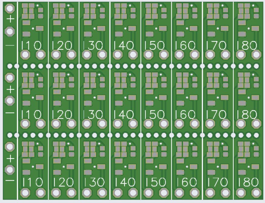
0.2" wide strips for autmomated assembly
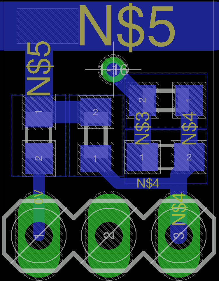
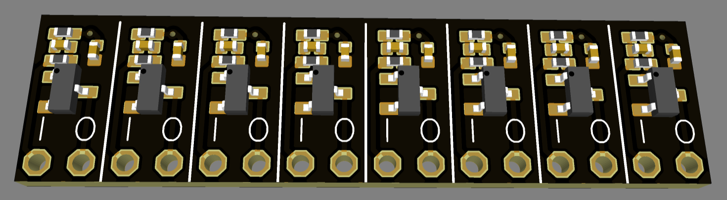
12/11/2021 at 22:20 • 12 commentsHere is an attempt in taking the strip concept and making it a bit smaller and easier to assmble.
I moved all components to the top to allow automated assembly. If we use an assembly service anyways, we can switch all the passives to 0402 and save a lot of space. The VCC power rail is now routed on the rear side, while there is a large groundplane for GND on both sides of the PCB, that will also help with shielding.
This new arrangment allows reducing the strip width to 0.2". Each element is a single inverter with pull up at the input. Multiple inverters can be combined to form wide input NOR2 gates in RTL.
A base resistor bypass cap is added to improve switching speed. There is no space for a schottky clamp diode, but probably the parasitics of the wiring scheme on a breadboard will limit the achievable speed a bit anyways. Each element also has a decoupling capacitor.
Open and still unsolved: How to connect to the power lines?
Some more renders below.
Edit: One could also fit a clamping diode in there. But then the text has to be moved to the rear side. Second from left:
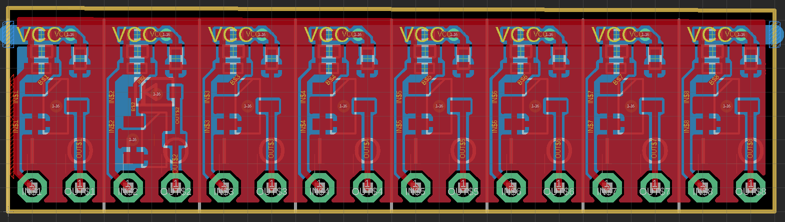
EDIT2: A version with drill-lines for easy separation
-
DCTL
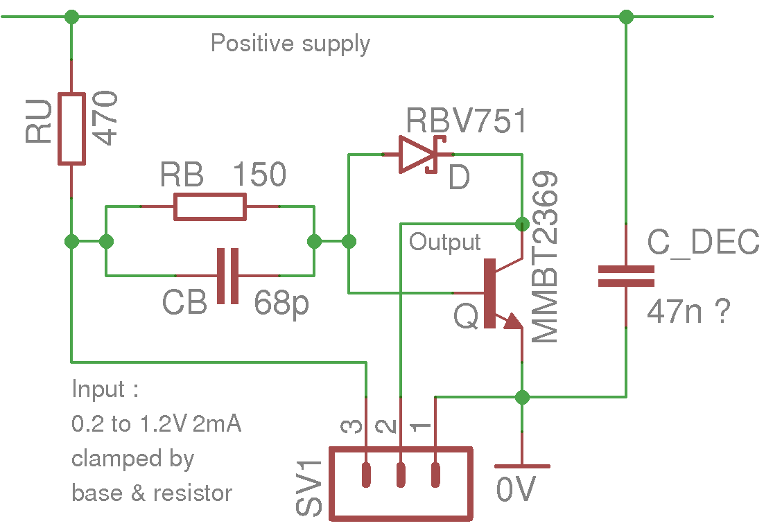
11/17/2021 at 13:17 • 0 commentsDCTL originally meant "Direct Coupled Transistor Logic", as described by @Tim on his great pages about the CDC6600 technology.
I have tried to increase the speed/power ratio with the help of a finely tuned base capacitor (C) and a Baker clamp diode (D) which seems to provide a propagation time of 2ns per inverter and/or a much better low-power performance. So this gives a new meaning to DCTL : Diode Capacitor Transistor Logic.
It's pretty easy to use yet quite unusual because each gate is only an inverter that provides an open-collector output, so it's all "OR-tied" logic, there is no dedicated inputs for each signal.
I have presented/introduced the individual gate in the description page of the project:
![]()
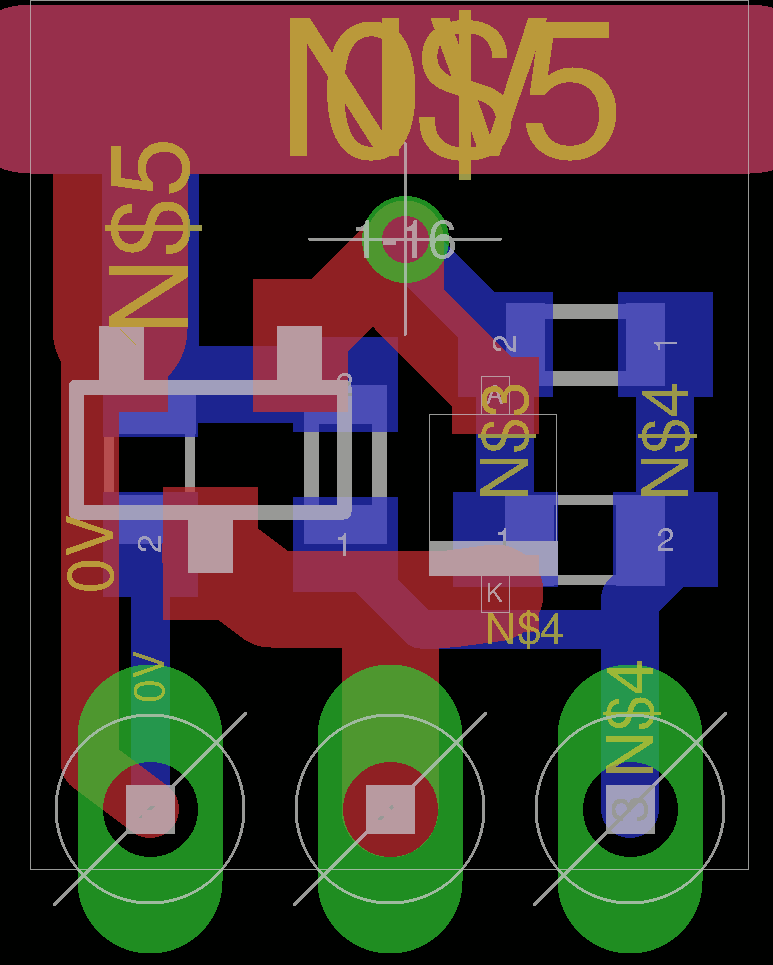
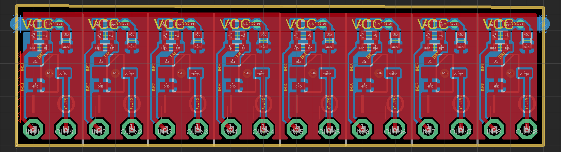
I have worked a bit more to make the PCB more compact:
![]()
There is only one via now, and all the passives are on the bottom layer, which could be pick&placed by machines. Here I only use 0603 parts but they could be changed to 0402 or anything you want.
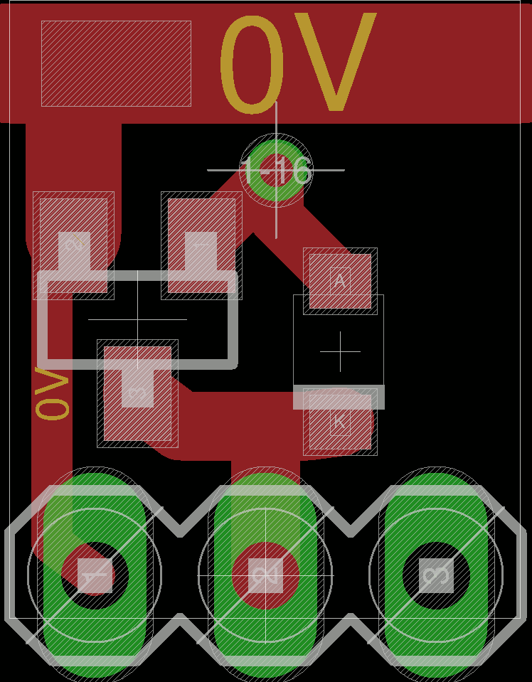
Here are the top and bottom layouts:
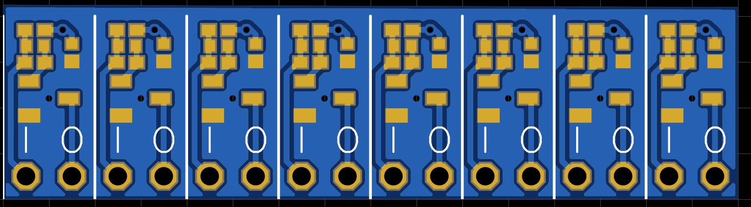
![]()
Now, the Ground/0V rail is on the top layer and directly connected to the PMBT2369's emitter.
There is some room at the right of the clamp diode.
![]()
The bottom layer has the passives (2 cap, 2 res) and the Vcc supply rail.
I added windows on the rails to make them easier to solder to sources/supplies.
Overall I have tried to reduce the "height" of the gate, compared to the first version. This makes the strips more densely packed and more cost-effective.
Logic strips
Attempting to lower the cost and augment flexibility of discrete logic designs.
 EDIT2: A version with drill-lines for easy separation