-
If you play with matches...
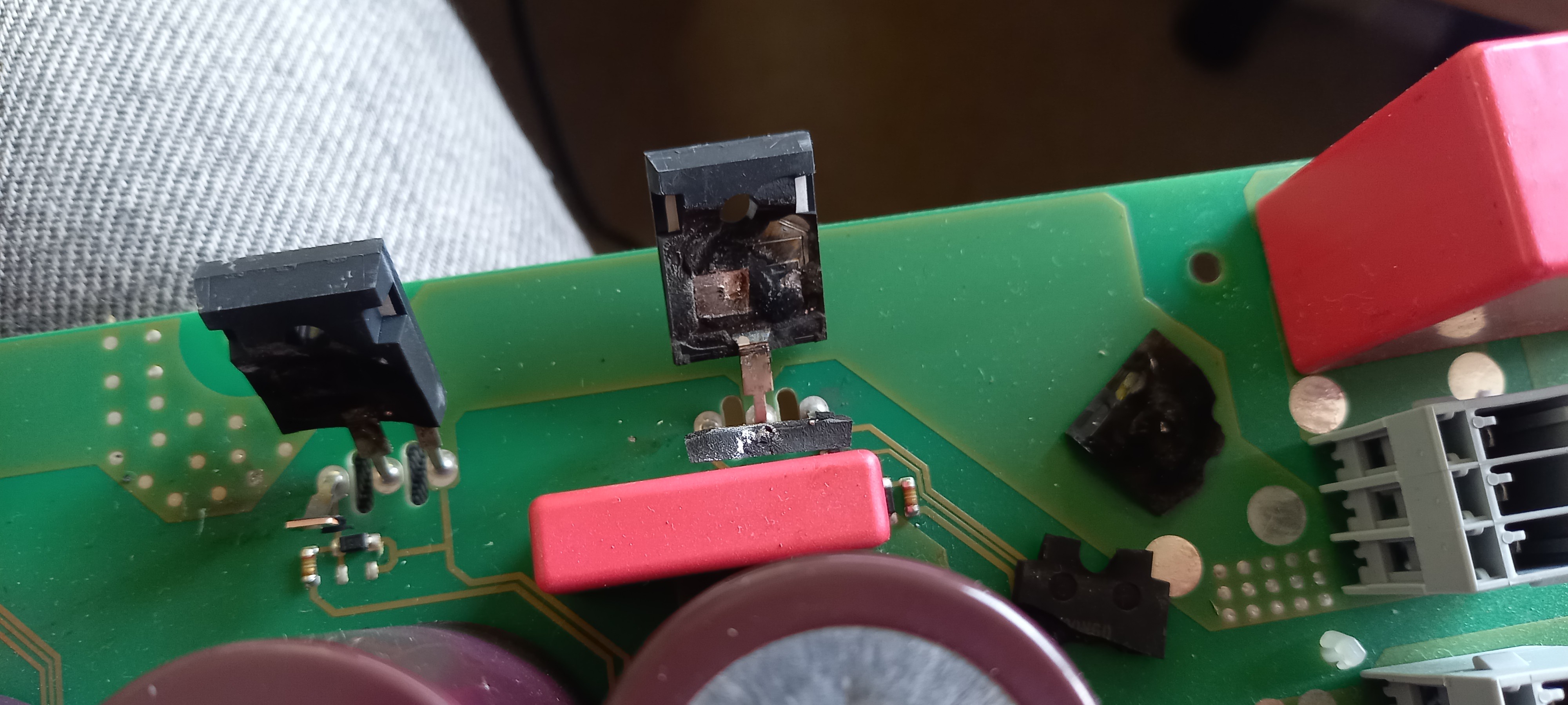
09/09/2022 at 13:56 • 0 commentsWell, the eye protection worked, but note to self: Next time, wear ear protection too. Discharging 500v, 2500uf of capacitors through two mosfets makes a loud bang. I think the microcontroller crashed because of all the interference when I tried to measure that side of the H bridge through an oscilloscope. Got the output voltage up to 100VAC though, with 500vdc on the capacitors. Well time to buy new mosfets and hope that the driver ICs are still all right.
![]()
-
Courage
09/05/2022 at 08:19 • 0 commentsNow working up the courage to charge the input capacitors to 300v+ and see if we can get 230vac output voltage and power something heavier. Stay advised.
-
First Light!
09/05/2022 at 08:01 • 0 commentsSo, on to the software side of things.
The software was reused from another project. It has some logging capability, a control loop which runs at 8khz in an interrupt. The LCDs and uarts and other peripherals are serviced in one freertos thread.
After fiddling with the PWM outputs for a while, that part worked as it should. Some safety features were added to make sure the PWM outputs would stop directly if something was wrong. The scariest thing is still that you are able to short circuit the input capacitors with the H bridge when something goes wrong. Nothing you can really do about that, just hoping the STM32F405 does not glitch out. If the DC bus voltage dips or rises too high, the outputs are disabled. When enabling the PWM outputs, a lot of power was used, I figured this was due to the system not having dead time between the high and low side of the H-bridge, so you get shoot through currents. After enabling dead time and fiddling with the amount, the problem was solved. For now, a dead time of 70*125ns=7us seems to work quite well, it has the lowest idling current.
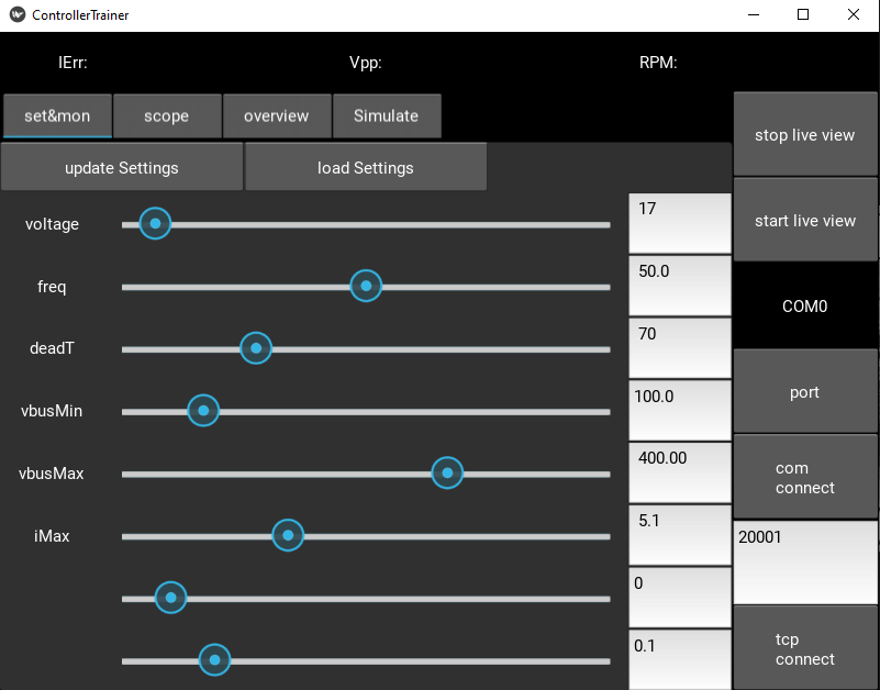
A PC GUI was made, SB2500-Trainer, to be able to change set points on the fly.
For now, the controlloop generates a Sinusoid waveform at 50Hz, with a variable amplitude which can be set in the SB2500 trainer. The voltage is slowly ramped up and down to make sure the transformer does not draw too much current at the start.
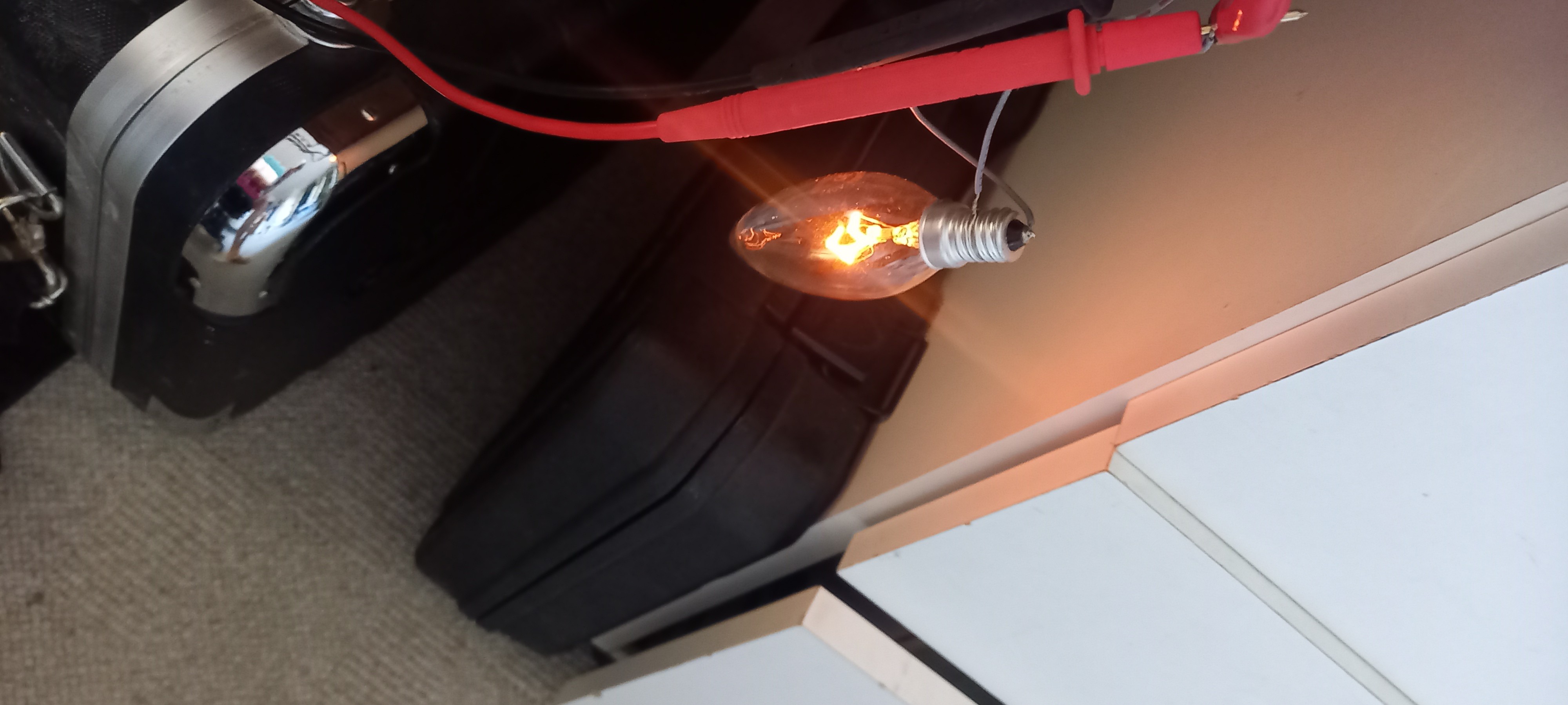
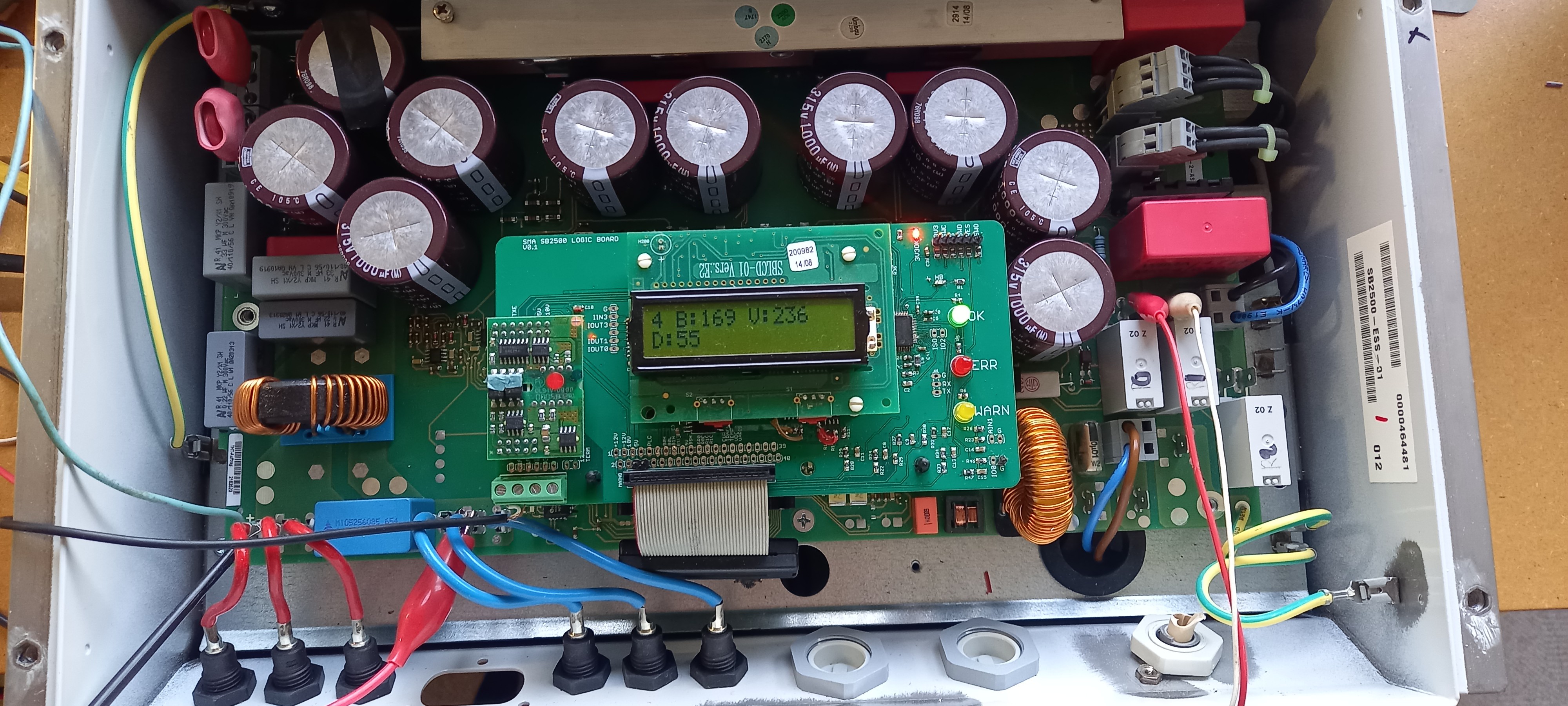
An input voltage of 170 volt was applied, and the whole contraption tested. I can now ramp up the output voltage to 100VAC and light a lightbulb with it! The inverter idles at 35 watt @ 170 volts input voltage, which is ok.
![]()
The controller PCB control GUI.
![]()
The lit lightbulb at 100VAC
![]()
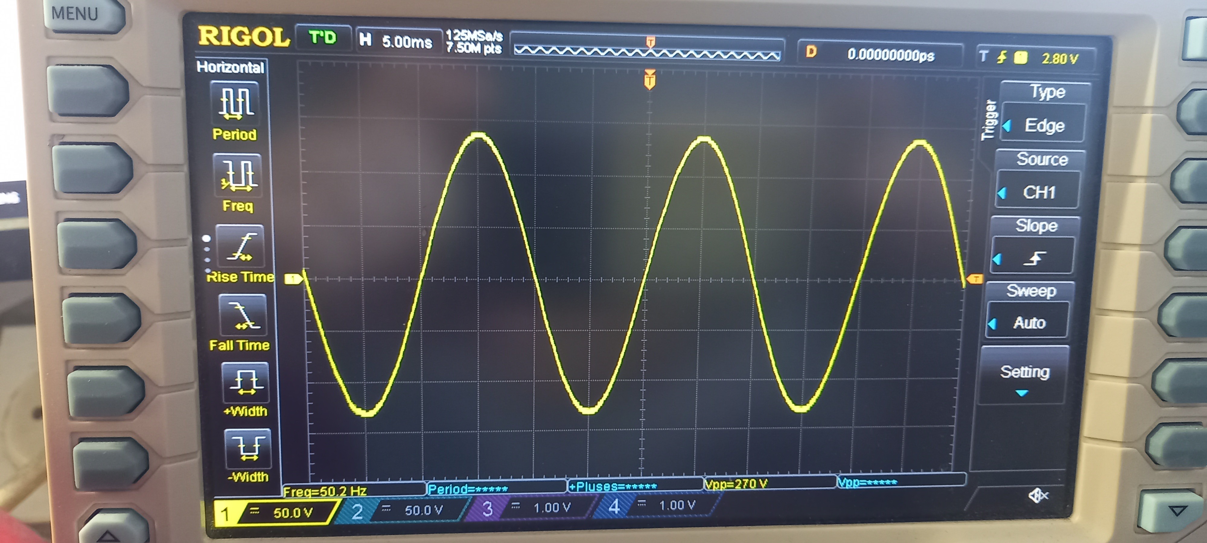
The output waveform, seems nicely sinussoidal.
![]()
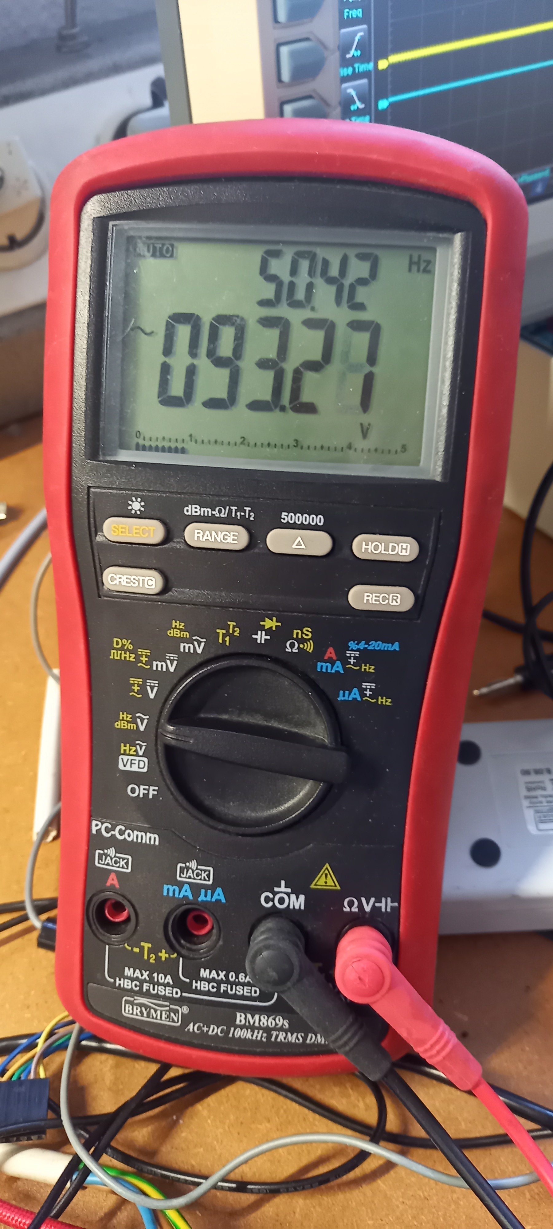
The output voltage and frequency.
-
PCB finished
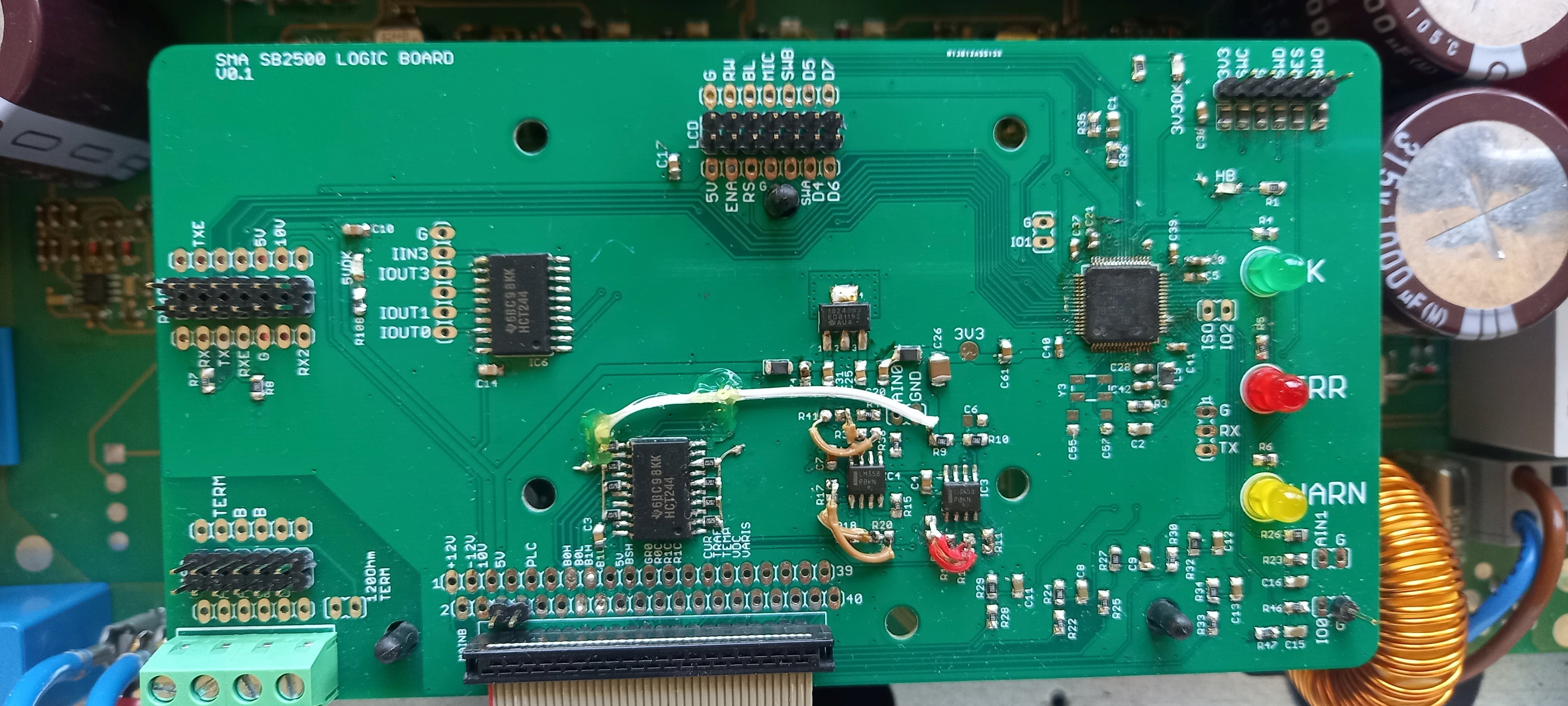
09/05/2022 at 07:50 • 0 commentsThe PCB was received and soldered together. The opamp plus and minus inputs were reversed sadly, so some bodge wires were necessary. The status of the PWM outputs was undefined as long as the CPU was not started and the bridge shutdown was active high, so the H-bridge would directly short circuit the input stage when power was applied to the input. A few extra pull down and up resistors were added to fix this mistake. The PWM outputs were also in the wrong order due to a mismatch on the input and output of the 74HCT244 IC.
But after fixing all these mistakes, the board functions as it should.
After setting up all the hardware in STM32CubeMX, a hello world could be displayed and some LEDs started blinking.
![]()
![]()
-
CubeMX design
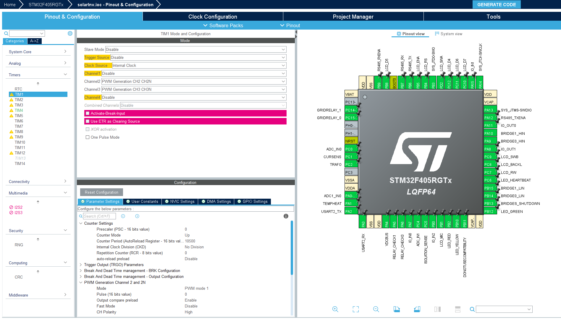
08/22/2022 at 18:57 • 0 commentsUsing STM32CubeMX the hardware peripherals of the STM32F405RG are set up. The most important hardware peripherals are timer 1, which drives the H-bridge at 16khz and the three ADCs, which sample the important signals at the moment where the signal is least disturbed, right before the PWM signal changes polarity. The Usart and the ADCs all use DMA for transfer, so as much CPU time is available as possible. After all ADC conversions are done, an interrupt is generated and the control loop can do it's thing.
![]()
-
PCB design
08/22/2022 at 18:49 • 0 commentsWith the pinout figured out, a new PCB design can be made. It is quite a lot simpler than the old design. It uses an STM32F405 microcontroller. Which is much more powerful than the 16 bit processor used before. But I already had a complete power electronics software design for this processor.
The PCB does not contain much except for the microcontroller, some resistor dividers to go from 5v to 3.3 volt. Some opamps to go from -2.5 - 2.5 volt to 0-3.3v and some logic to voltage shift from 3.3 to 5v.
The PCB was kept flexible for when there would be pinout mistakes, and the extra pin headers next to all the main headers can be used for easy signal reading. The design can be found on Github.
The PCB is ordered at PCBWay, pictures will be shown in another log entry.
![]()
-
Pinouts, pinouts, pinouts
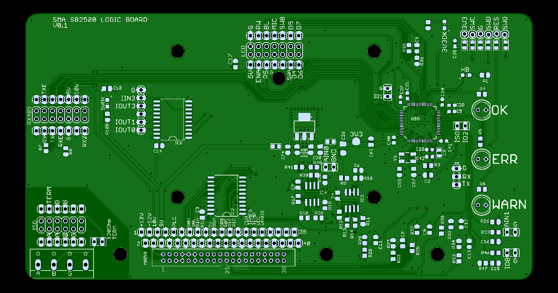
01/16/2022 at 17:49 • 0 commentsToday, the pinout of the 40pins connector was checked. The inverter was powered up at the DC side through a isolation transformer and the voltages on the pins checked. The pinout of all the daughter boards were determined (communication and LCD daughterboard), as far as possible. The size measurements of the Logic board were taken for a new PCB design. See Github for the latest information.
It will be possible to reuse the LCD board and the isolated RS485 communications board, which is great.In the end, it will be easier to recreate the Logic board then to reuse it. As you need to buy a special programmer to be able to program the DSP, and this programmer will cost just as much as a complete PCB design. And I much prefer the STM32CubeIDE anyways.
-
Start
01/02/2022 at 13:34 • 0 commentsThis is going to be exiting. High voltages, grid creation, old microcontroller development studios. I tried to document the insides of the inverter as well as possible. Check the Github readme.md for the most recent information.
Grid Tie inverter SMA Sunny Boy SB2500 openlogic
Try to reuse a SMA Sunny Boy 2500 Grid Tie inverter as an off grid inverter
 ClimbinElectronics