As you can see, the name has changed:
 This is because it doesn't seem that there's a merge between a linear slide potentiometer and a rotarty encoder, so this device is now just "Tetrinsic". Actually, drop the "encoder" since I my other project titles aren't "#SecSavr Suspense [gd0105] 3D Printer" or "#T^2 Tiles [gd0095] Robotic Wall". Consistency. On the other hand, maybe I should actually be doing that so it's more obvious what the project is. I feel like my project titles would get pretty long if I did that though. Are my hover descriptions not good enough?
Anyway, the PCB.
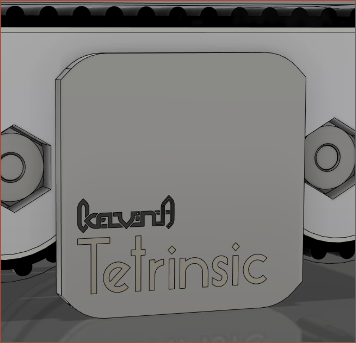
It's a 15.5mm square. JLCPCB will let me have a thickness as low as 1mm whilst keeping the white and the same price, so I've done that. This makes the model 18.85mm thick, so maybe I could get 19.5mm minimum spacing. This assumes that I could use a 2 layer PCB though. For the artistic side, I've decided to have my logo as silkscreen and project name as a plated copper pad. Obviously, this will only work if I don't need traces there.
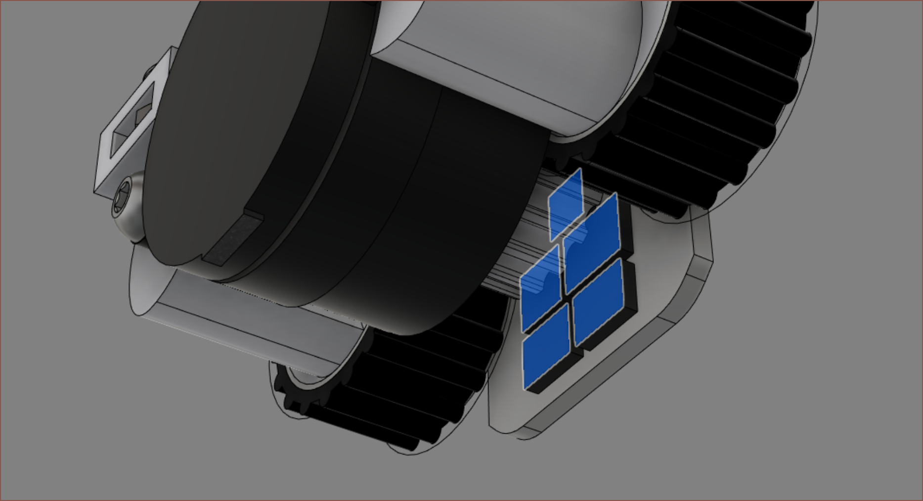 It's pretty close, but there's enough surface space for the 5 chips. I also dug around the datasheets to deduce that the MP6543 needs 4 output pins and the 24-bit ADC needs 5? Looking at the datasheet, I'm hoping that I can have the master clock and the SPI clock connected together, reducing my required output pins to 4.
 I'm thinking of soldering the 3 sets of flexible cables straight to the 4mm of space on either side, and passive components fit around the available space around the magnet sensing chip. One is the cable from the motor, and the other two are the daisy-chain link cables. One cable (likely the motor) would have to go over another one of the cables to fit. I expect that I'd need at least 4 traces in the cables if I'm able to find a place to solder power wires for the motor.
[Goes back to JLCPCB]
Oh nvm as soon as I select "lead free" finishing process, I'm either looking at a decently priced green or 4x for white. That's fine until 4 layers where 15 white PCB's is $77, so I should fully expect to silkscreen everything so that I (hopefully) only need 2. Wait... silkscreen everything? Silkscreen is white, right. How white?
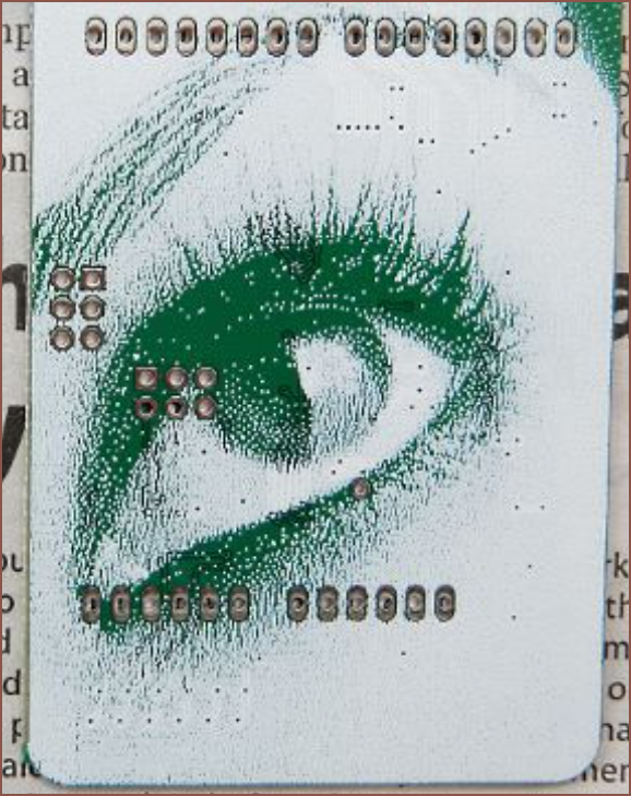 White enough for my science. Wait, that means that I could totally get "white PCBs with green silkscreen" by just inverting the normal silkscreen. I'll remember that.
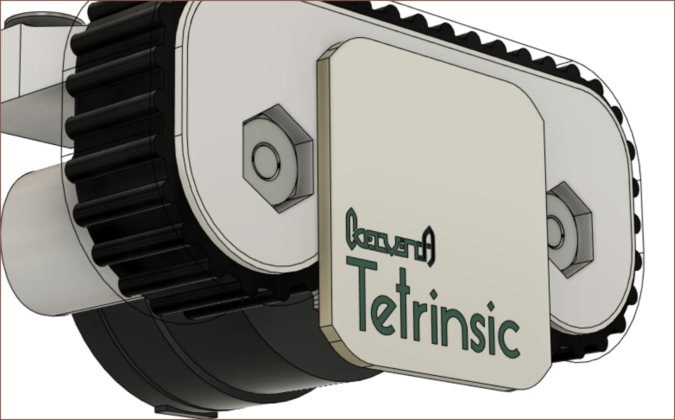
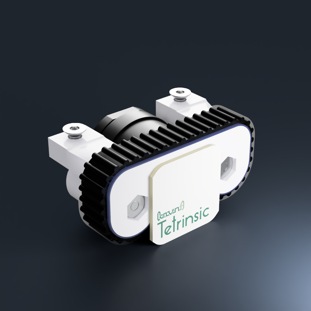 I wonder how far off this render is from looking like the "future first proof of concept" now. That was a roundabout way of saying that I think I'm getting close to a design that will actually exist in the real world.
[22:44]
This is what 19.5mm spacing looks like in the #Tetent Timespy [gd0136]:
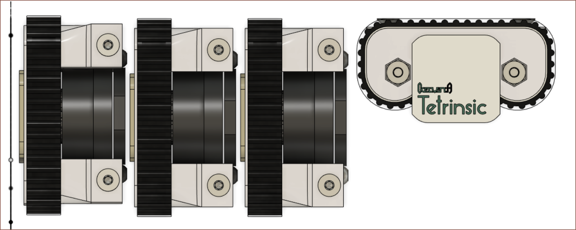 It's going to be pretty close, but I'd be pretty satisfied if I can get this. Actually, I'm somewhat suprised that I can DIY something this unproven yet so professional looking run. I wonder if I should add 3 dots in the top right to make the board look even more advanced though.
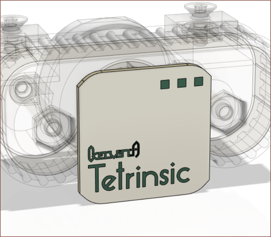 It certainly looks a lot less plain.
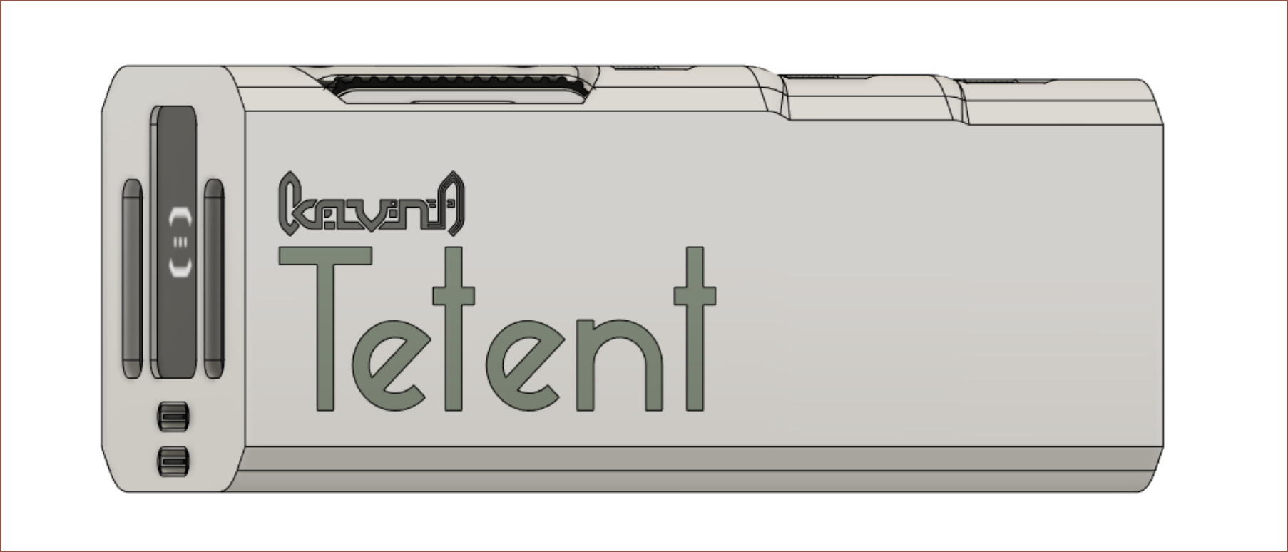 I'll pass because the branding looks perfectly good as is on Tetent.
 kelvinA
Discussions
Become a Hackaday.io Member
Create an account to leave a comment. Already have an account? Log In.