 Epsilon
-
BoxLambda: Make, Tcl and Bender Build System
07/04/2022 at 10:03 • 0 commentsThe Hello World build in the previous post is a GUI-driven Vivado project. I would like to upgrade to a hierarchical, command-line-driven build system. In a command-line-driven build system, it’ll be easier to automate tasks and it’ll be easier to integrate tools that are not part of Vivado, such as Cocotb and Verilator.
Terminology and References
- CocoTB: A Python-based framework for digital logic verification. See https://www.cocotb.org/.
- Constraints File: A constraints file specifies the mapping of the top-level HDL module’s input and output ports to physical pins of the FPGA. It also defines the clocks used by the given design. See https://digilent.com/reference/programmable-logic/guides/vivado-xdc-file.
- EDA tool: A software tool to design electronic circuits, e.g. Vivado.
- IP-XACT: An XML format that defines and describes individual, re-usable electronic circuit designs to facilitate their use in creating integrated circuits.
- IP Package: A Vivado file encapsulating an IP component using the IP-XACT file format.
- Makefile: A file used by the Make utility, defining a set of tasks to be executed, and defining dependencies between tasks. Makefiles are commonly used to create build systems.
- Memory File: A file containing the initial contents of a Block RAM instance used in an FPGA design.
- OOC: Vivado’s OOC mode or OOC flow lets you synthesize, implement, and analyze design modules in a hierarchical design.
- Tcl: The defacto standard embedded command language for EDA applications.
- Verilator: A tool that converts Verilog to a cycle-accurate behavioral model in C++ or SystemC. The performance of the generated behavioral model is generally much higher than that of a traditional event-driven simulator. See https://www.veripool.org/verilator/.
Vivado IP Packages
Vivado has an embedded, Tcl-based command-line interface. For every GUI action, there’s an equivalent Tcl command or set of commands. My initial approach to creating a build system was to use a combination of Makefiles and Tcl scripts to get Vivado to generate a so-called IP Package for each component. These IP Packages then constitute the building blocks of our system: IP Packages can be aggregated into bigger IP Packages. A top-level project build aggregates IP Packages into an SoC.
This approach has some advantages:
- It’s hierarchical: A big SoC build is (recursively) broken down into manageable components.
- It doesn’t introduce any new tool dependencies other than GNU Make.
Along the way, I learned that Vivado IP Packages also have some disadvantages:
- SystemVerilog is not supported at the top-level, i.e. I have to create Verilog wrappers around SystemVerilog-based components. That’s not the end of the world, but it does feel like a step backward.
- Vivado IP Packages come in a standard format called IP-XACT. If I want to create a flat list of files that make up a project, e.g. to feed to Verilator or Cocotb, I need a tool to extract information from IP-XACT files. I was able to find one tool, called Kactus 2, but that appears to be a full-fledged graphical EDA application, rather than a command-line utility. As long as I can’t easily interface to IP-XACT files, I’m locked into Vivado and won’t be able to use third-party tools like Verilator or Cocotb.
That last item is a deal-breaker for me. I start looking for other options.
FuseSoc
https://fusesoc.readthedocs.io/en/stable/
FuseSoc is a package manager and build system for HDL code. HDL builds can be retargeted from one EDA tool to another with the flip of a switch, so to speak. The tool is already in use by projects such as Ibex, and it looks very promising, so I decide to give it a shot…
Creating a so-called FuseSoc core file, a manifest defining the component, is easy enough. Once you have such a core file, you can instruct the tool to generate, for instance, a Vivado or a Verilator build for it. The problem is, I have no idea how it works. When I kick off a Fusesoc Verilator build, I get a nice OK message at the end, but I have no idea what that means, or what happened along the way. It’s also not clear to me how to customize the flow to accommodate use cases that are not already built into the tool. I see there’s a hook mechanism, but it’s not documented. Overall, I’m not in control of this build system. I just have to hope that FuseSoc does the right thing.
Advantages:
- Handles dependency management as well as EDA tool interfacing (through Edalize).
- Supports many different EDA tools.
- Very easy to retarget a build from one EDA tools flow (e.g. Vivado synthesis) to another (e.g. a Verilator build)
Disadvantages:
- Not sufficiently documented.
- Not clear how to customize for use cases that are not built-in. E.g. How to integrate Cocotb?
- Behind-the-scenes magic: The user of the tool is not in the driver’s seat.
- Additional tool dependencies and associated learning curve: FuseSoc itself, Python, etc.
FuseSoc has a lot of potential. It works for a lot of people (e.g. Ibex), but in its current form, it’s not a good match for me.
Bender
https://github.com/pulp-platform/bender
Where FuseSoc aims to control the entire flow itself, Bender aims to do just one thing: Dependency Management for hardware design projects. Bender itself is not a build system. It’s a tool that feeds the build system.
Central to Bender is the package manifest bender.yml. In the manifest, you specify the HDL sources that make up the package, dependencies, include paths, targets (e.g. synth, sim), and associated defines. A package directory is a directory containing a bender.yml file. When you run bender in that directory, you can ask it to generate a flat list of all the sources from the current package, and the packages it depends on. Optionally, it can generate that list, plus any defines associated with a given target, as a Tcl script. This makes integration with Vivado very easy.
You can of course do all those things yourself using Makefiles and shell scripting, but it’s very tedious, and you know you’re reinventing the wheel for the umpteenth time. Bender absorbs a lot of the hassle of creating a build system, but you are still in the driver’s seat.
Advantages:
- Dependency management is elegantly taken care of.
- A tool that feeds the tools. Easy to integrate into a custom build flow.
- Minimal learning curve. The info in the README is all you need.
- Minimal tool dependency: bender is a single binary executable.
Disadvantages:
- Doesn’t do much in way of EDA tool interfacing. That’s left up to the build system creator.
That’s good enough for me. I’m going for a Makefile-Tcl-Bender combo build system.
The Build System
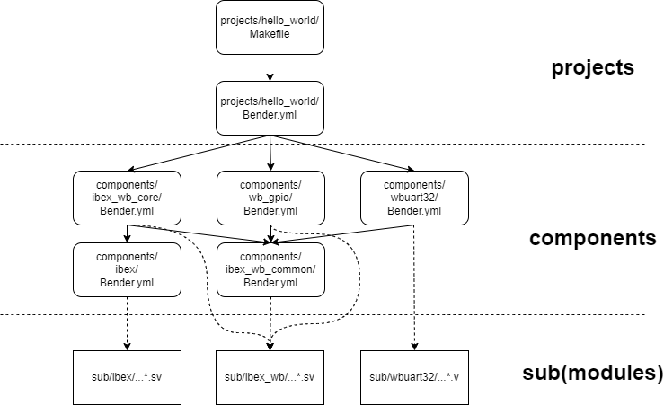
![Project View of the Build System]()
Project View of the Build System
The build system has three layers:
- The Project Layer (top): Hello World is an example project. A project is the top layer of the build system. The bender.yml manifest contains the top-level files of an SoC build, the project’s .xdc constraints file, memory files used by the SoC, and a list of components the project depends on.
- The Component Layer (middle): Components are the middle layer of the build system. They are the building blocks of an SoC. A component’s sources, defines, and dependencies are defined in a bender.yml manifest. A component gets its HDL sources from its rtl/ subdirectory and/or from sub/, the submodule layer. I’m considering each Wishbone Bus Master or Slave a component.
- The Submodule Layer (bottom): Submodules are the bottom layer of the build system. They are the Git Submodules that BoxLambda is referencing, as discussed previously.
I reshuffled the repository’s directory structure a bit to reflect the three layers:
boxlambda
├── build_sys
├── projects
│   └── hello_world
├── components
│   ├── ibex
│   ├── ibex_wb_common
│   ├── ibex_wb_core
│   ├── wb_gpio
│   └── wbuart32
└── sub    ├── ibex    ├── ibex_wb    └── wbuart32
The Project Build Makefile
A project directory, such as projects/hello_world/, contains a top-level Makefile, with the following build targets:
- dryrun: Generate a Vivado project, but don’t build it.
- synth: Generate a Vivado project and synthesize it.
- impl: Generate a Vidado project, synthesize it, and implement it.
- run: Download the generated bitstream file to the target. Note: The script this build target executes is configured for my WSL-based setup. It may need customization for other setups.
- clean: Remove all generated files in the current directory and subdirectories.
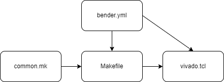
What happens when you run make synth
When you run make synth, the following happens:
- Make runs a bender script command.
- The bender script command processes the current directory’s package manifest (bender.yml), as well as the package manifests of any dependent components.
- The bender script command emits a list of all the HDL sources that make up the project.
- Make feeds this file list, along with a .xdc constraints file and any .mem memory files, into a vivado.tcl script.
- The vivado.tcl script generates a Vivado project file containing all the HDL sources, constraints, and memory files.
- The vivado.tcl script kicks off synthesis and generates timing and utilization reports when synthesis is complete.
When you run make impl, the same thing happens, but after completing synthesis, the vivado.tcl script proceeds to kick off implementation and bitstream generation.
![The Build System Files - arrows indicate information flow]()
The Build System Files - arrows indicate information flow.
The relevant files are linked below. To avoid repeating identical rules and variables across Makefiles, a build_sys/common.mk include file is created which contains all reusable Makefile logic.
A Component Build
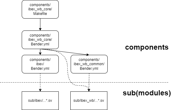
Components can also be synthesized, in Out-Of-Context (OOC) Mode. In OOC mode, the synthesizer is made aware that the top-level module’s input and output ports are not tied to chip pins, i.e. that this is just a partial build. A component Makefile works the same as a project Makefile, but with an OOC Makeflag set and propagated to Vivado.
![Component View of the Build System]()
Component View of the Build System
About Memory Files
Memory files used by an FPGA build are typically generated from software. It would be annoying to have to build the hello world program, to generate a memory file, and then build the FPGA in a separate step. As a rule, a build system should start from sources, not from build artifacts created separately by other build systems.
To combine the software and FPGA build steps, the build system has a pattern rule for .mem memory files. Whenever the build system encounters such a file as a dependency, it goes to that file’s directory and runs make there, to make sure that the .mem file gets generated.
#Pattern rule for memory files: Go to the memory file's directory and run Make there.
%.mem : force
	$(MAKE) -C $(@D)
The current mechanism just assumes that the default rule in the recursive make will do the right thing. It’s a bit crude, but it’s a start.
Second Iteration complete
The second iteration is complete. We still have a working hello world proof-of-concept project, but now it’s generated from an actual command-line-driven build system.
I did make a small change to hello.c: After printing out Hello world, the program goes in a loop toggling the LEDs. This way, the program exercises the GPIO core as well as the timer core in addition to the UART core.
To build the project:
- Install the prerequisites.
- git clone https://github.com/epsilon537/boxlambda/,
- cd boxlambda
- Switch to the make_and_bender tag: git checkout make_and_bender.
- Get the submodules: git submodule update –init –recursive.
- Build the project:
- cd projects/hello_world
- make impl
- Start Vivado and download the generated bitstream to your Arty A7-35T: projects/hello_world/generated/project.runs/impl_1/ibex_soc.bit
Interesting Links
In the Beginning Was the Command Line : A famous essay by Neal Stephenson about command-line interfaces vs. GUIs, closed vs. open source, and Apple vs. Microsoft, among other things.
-
First Contact: Hello World!
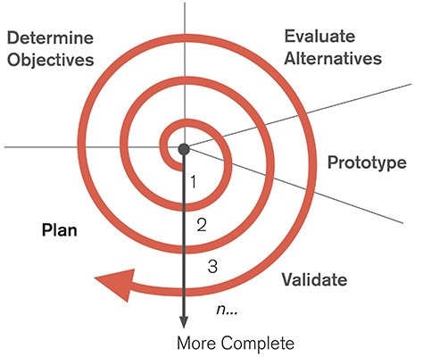
06/19/2022 at 12:21 • 0 commentsAfter the IRQ post, I started looking for the shortest path to get something simple to work. The idea is to bring up something small, an embryonic version of the project. Iteratively, I then keep growing this small system until I end up with a system that meets the goals. After each iteration, the project should be functioning somewhat better than it was before.
![Iterative Design Spiral]() Iterative Design Spiral
Iterative Design SpiralHalfway through the first iteration, I realized I needed to figure out my git workflow, or I wouldn’t be able to commit and push my work. Hence, the previous post.
The Tiny System
Now, back to taking that first step: I want to bring up the RISCV processor and run a test program on it that can print to the serial port. In other words, I want to run a ‘Hello World!’ program on my Arty A7-35T. Doing so will give us access to print-style debugging, which is sure to come in handy down the road.
To get to ‘Hello World’, I need to put together a tiny system consisting of the following cores:
- Ibex RISCV processor (to run the SW).
- Internal memory (to hold the SW).
- wbuart32 (serial port console).
- A Wishbone interconnect to connect the processor to memory and the UART core.
The Ibex repository includes an example system, called Simple System, that’s similar to the initial system I have in mind, but it does not include a Wishbone interconnect. It shouldn’t be too hard to add a Wishbone interface to Ibex myself, but first I should take a look around to see if a Wishbone-for-Ibex solution already exists. Lo and behold it does:
https://github.com/batuhanates/ibex_wb
The ibex_wb SoC Cores
The ibex_wb SoC includes the following cores:
- ibex: The RISCV CPU core. The ibex_wb project was pointing to a 3-year-old version. I modified it to use the BoxLambda ibex fork.
- wbuart32: UART core. The ibex_wb project was pointing to a 3-year-old version. I modified it to use the BoxLambda ibex fork.
- riscv_dbg: JTAG debug interface. This is a pretty complex core. I ifdef’d it out for the time being. To be revisited.
- wb_gpio: GPIO core, for sampling buttons and switches and driving LEDs.
- wb_timer: A timer core, so we can do things like *usleep()* from software.
- spramx32: Single Port RAM. To be replaced at some point by a Dual-Port RAM.
- core2wb/core_if/wb_if/slave2wb: Ibex to Wishbone interfacing logic.
The ibex_wb/soc/fpga/ directory has an SoC build for Cyclone V, the Arty A7-100T, and the Nexys4-DDR. I added an arty-a7-35/ subdirectory, using the Nexys4-DDR SoC code as a starting point.
This ibex_wb SoC is pretty much a perfect match for the initial system I had in mind. How convenient!
The ibex_wb SoC Software
The software is located in the ibex_wb/soc/fpga/arty-a7-35/sw/ directory:
- libs/soc/ contains drivers for the cores
- examples/ contains example programs. I tested the hello and the blinky programs.
ibex_wb/soc/fpga/arty-a7-35/sw/examples/hello/ contains a simple Makefile to build the software and generate a hello.mem file. hello.mem holds the initial contents of the internal memory of the SoC. The file’s contents are included in the FPGA bitstream.
The same directory also contains a linker script, link.ld, that specifies how much memory is available, and where all the code, data, and stack should go:
OUTPUT_ARCH(riscv)
...
MEMORY
{
	ram         : ORIGIN = 0x00000000, LENGTH = 64K
}

_min_stack      = 16K;   /* minimum stack space to reserve */
_stack_start	= ORIGIN(ram) + LENGTH(ram) - 4;
...
SECTIONS
{
	.vectors : ...

	.text : { ...

	.data : { ...

	.bss : { ...

	.stack (NOLOAD): {
		. = ALIGN(4);
		. = . + _min_stack ;
		. = ALIGN(4);
		stack = . ;
		_stack = . ;
	} > ram    ...
}
ORIGIN should be set to match the CPU’s boot vector. On the FPGA side, the boot vector is specified during CPU core instantiation. I currently have it set to 0 in ibex_soc.sv:
wb_ibex_core wb_ibex_core (
.instr_wb     (wbm[COREI_M]),
.data_wb      (wbm[CORED_M]),
.test_en      (1'b0),
.hart_id      (32'h0),
.boot_addr    (32'h0),
...
Synthesizing the SoC
The original ibex_wb repository appears to be dormant or abandoned in an unpolished state. There’s no documentation, Makefile, or other type of project file that specifies how the SoC should be synthesized. Luckily, SystemVerilog is fairly self-describing. Once you’ve found the top-level, usually a file with the word top in it, it’s a matter of recursively adding referenced modules until all references have been resolved. Easy enough. I added all files in a Vivado project file. It’s checked in here:
https://github.com/epsilon537/boxlambda/tree/develop/fpga/vivado/hello_world
Simulating and Running the SoC
Initially, nothing worked, of course. There are always bugs. There were bugs in the link.ld script, in the Vivado constraints file, in the top-level file ibex_soc.sv… I even managed to make a mistake in the simple hello.c test code. Guess what’s wrong with this code:
int main(void) {
	uart_init(&uart0, (volatile void *) PLATFORM_UART_BASE);
	uart_set_baudrate(&uart0, 115200, PLATFORM_CLK_FREQ);
	uart_printf(&uart0, "Hello World!\r\n");
	return 0;
}
The problem is that main() returns after printing Hello world. Returning from main() causes the system to restart. As a result, I was only seeing HHHHH… on the serial port. The system was restarting before the rest of (H)ello world made it out to the serial port. As a fix, I added a while() loop after the uart_printf() statement.
I was able to find these issues by loading the design in the Vivado simulator and looking at the waveforms (CPU bus transactions, state of the UART transmit FIFO, etc.). Getting the simulation going was not straightforward either, however. Vivado tripped over the compilation of a .c file, code-generated by Vivado itself. By looking at the references in the failing code, I was able to trace the issue back to a specific SystemVerilog code snippet in the ibex code base. I filed a bug report for it:
https://github.com/lowRISC/ibex/issues/1679
In the BoxLambda ibex fork, I disabled that code fragment (the fragment isn’t critical for the execution of the processor) and now the simulation is working fine.
After sorting out the above issues, I can finally load the FPGA bitstream onto my Arty-A7, and I’m greeted by this happy message:
![Hello World! from ibex_wb on Arty A7-35T]() Hello World! from ibex_wb on Arty A7-35T
Hello World! from ibex_wb on Arty A7-35TFirst Iteration complete
The build is rough around the edges. Vivado reports synthesis and implementation warnings. The .xpr project file is just a blob of files without organization. But I do have a tiny, working project. The first iteration is complete. Feel free to try it out:
- Install the prerequisites.
- git clone https://github.com/epsilon537/boxlambda/,
- cd boxlambda
- Switch to the hello_world tag: git checkout hello_world.
- Get the submodules: git submodule update –init –recursive.
- Build the software:
- cd fpga/ibex_wb/soc/fpga/arty-a7-35/sw/examples/hello
- make
- Open project file fpga/vivado/hello_world/hello_world.xpr in Vivado.
- In Vivado, start a simulation, or synthesize the design and generate a bitstream to load onto your Arty A7-35T.
Architecture Diagram updates
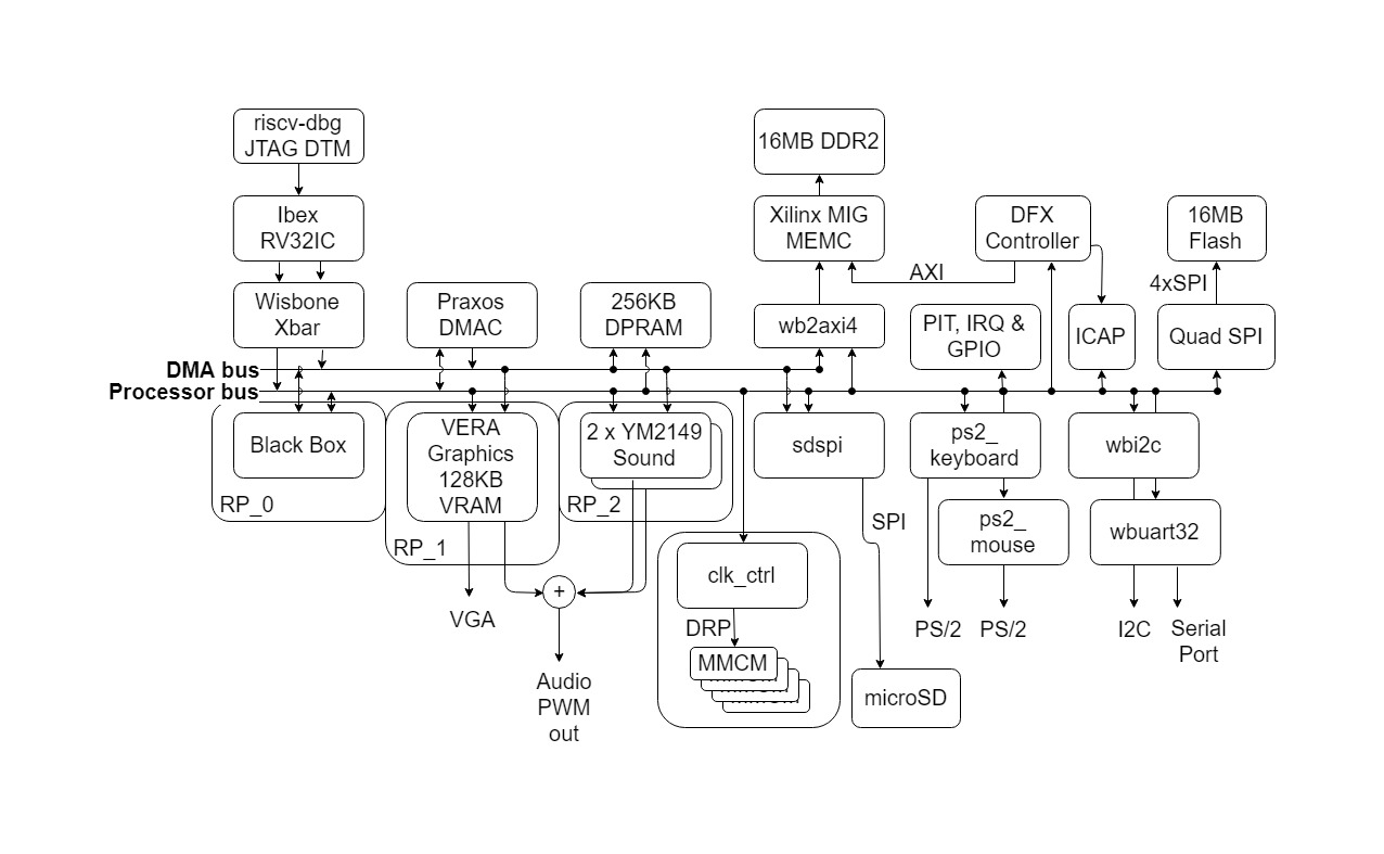
As it turns out, my initial Architecture Diagram was more accurate than the correction in the follow-up post. The timer is not internal to the Ibex core. It’s just another core on the Wishbone bus. The same thing goes for the riscv-dbg core. Here’s the updated diagram. I highlighted the changes.
![BoxLambda Architecture Block Diagram (Nexys version)]() BoxLambda Architecture Block Diagram (Nexys version)
BoxLambda Architecture Block Diagram (Nexys version)FPGA Utilization updates
The riscv-dbg core is not a trivial module. It contains quite a bit of logic as well as internal memory. Its footprint needs to be taken into account in the utilization tables.
Estimated FPGA Resource Utilization on Nexys A7-100T:
Estimated FPGA Resource Utilization on Arty A7-35T:
Interesting Links
https://opentitan.org/: It doesn’t take a lot of digging to find your way from the Ibex project to OpenTitan. OpenTitan is a very complete ecosystem for RISCV-based SoCs. OpenTitan is using the TileLink bus protocol rather than Wishbone. To be honest, discovering OpenTitan and TileLink triggered a bit of an existential crisis for BoxLambda. Wouldn’t it be better for BoxLambda to use TileLink and OpenTitan as a baseline instead of Wishbone and the collection of components? I eventually decided to stay the course. BoxLambda will hopefully be a long-running project and, now and then, cool new stuff is bound to cross my path. It wouldn’t be good for the project to switch directions every time I come across another interesting project.
-
Git Workflow and Setup
06/12/2022 at 09:07 • 0 commentsGit Workflow
BoxLambda is a GitHub project that depends on a bunch of other GitHub projects. How do I pull it all together under one umbrella? I don’t just want to copy somebody else’s code and submit it into my repository. That would be impolite and I would lose all tracking with the original project. I want to be able to track the original project, make my own changes, and integrate the project into the BoxLamba repository.
Git submodules are a great solution for this situation. Submodules allow you to keep a git repository in a subdirectory of another git repository. When you’re making changes inside the submodule subdirectory, those get committed to that submodule’s repository. The parent (supermodule?) repository on the other hand, just tracks submodule commits. From git’s point of view, the submodule subdirectory is not a subdirectory, it’s a file with a reference to a git repository and a specific commit within that repository.
OK, I guess that sounds pretty confusing. Here’s a much better explanation:
https://git-scm.com/book/en/v2/Git-Tools-Submodules
Directories and branches
I’ll be using the following directory layout in the BoxLambda repository:
boxlambda/doc
boxlambda/fpga/ibex (ibex fork git submodule)
boxlambda/fpga/wbuart32 (wbuart32 fork git submodule)
boxlambda/fpga/<other FPGA git submodules>
boxlambda/fpga/<BoxLambda specific FPGA files that don't fit in any of the submodules> boxlambda/sw/<SW fork git submodules>
boxlambda/sw/<BoxLambda SW files that don't fit in any of the submodules>
Each of the git submodules is a fork of a GitHub project discussed in earlier posts. For example, boxlambda/fpga/ibex/ contains my ibex fork, not the original ibex repository.
In each of the forked submodules, two branches are relevant:
- master: I’m keeping the master branch in sync with the master branch of the repository I forked from. Having this branch makes it easy to pull in updates as well as to submit the occasional pull request to the original project.
- boxlambda: On this branch, I’ll be making changes for BoxLambda.
In the BoxLambda repository itself, I have the following long-running branches:
- master: I will submit releases to this branch. The master branch should always be in good shape.
- develop: This is where the work is happening. Things will be in flux here. This branch will not always be in good shape.
- gh-pages: This branch holds the BoxLambda Blog files. GitHub Pages are by default on the gh-pages branch of a GitHub project.
- boxlambda-gh-pages-wip: This branch holds work-in-progress Blog updates. This branch also contains some config file modifs specifically for local previewing, which is why this is a long-running branch, rather than a topic branch. When updates are ready for release, I merge them to gh-pages.
I already pushed this structure to GitHub. Feel free to take a look around:
https://github.com/epsilon537/boxlambda
GitHub does a great job displaying submodule subdirectories:
https://github.com/epsilon537/boxlambda/tree/develop/fpga
My Setup
I’m working on Ubuntu WSL on Windows 11. It would be better to work on a native Linux box, but I need to be on Windows for other work, so WSL it is.
WSL is working well for me. My C: drive shows up as /mnt/c under Linux, so sharing files between Linux and Windows is easy. The clipboard also works seamlessly between Windows and Linux and the Linux apps run right inside the Windows desktop.
Xilinx’s Vivado installation was straightforward. As a test, I built Ibex’s Arty A7 example using the README instructions. Synthesis, implementation, and bitstream generation went just fine.
However, when I tried to program the bitstream on my Arty A7 board, connected via USB, I noticed that Vivado wasn’t detecting the board. Ugh. WSL is not perfect after all.
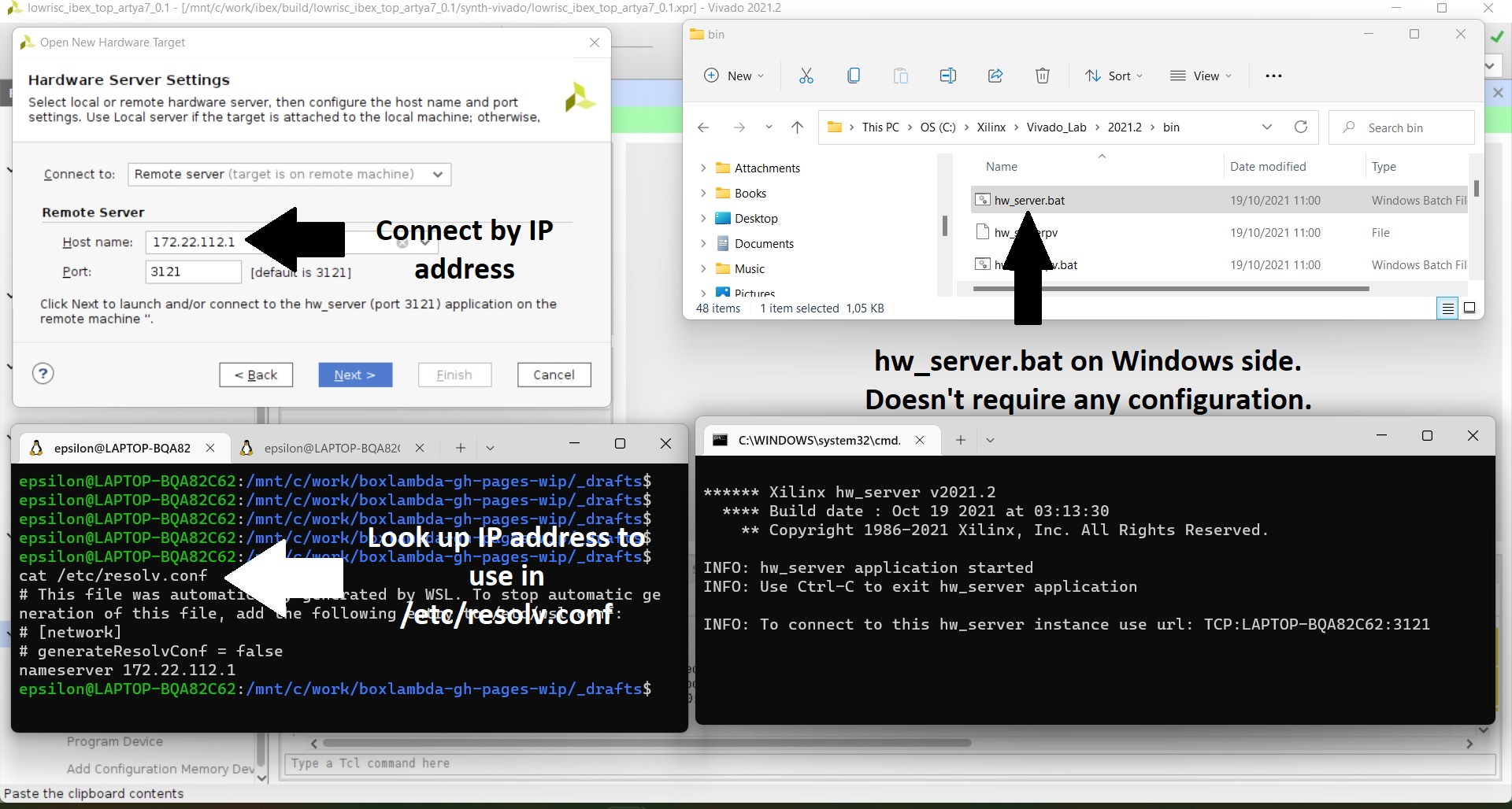
As a workaround, I installed the Vivado Lab edition on the Windows side. Unlike a regular Vivado installation, the Lab edition is very small. It’s intended for lab machines physically connected to FPGA targets. With the Vivado Lab edition on Windows, I can launch the hardware server, hw_server.bat, on the Windows side. The hardware server on the Windows side is detecting my USB connected target just fine. I can connect to the hardware server from Vivado on the Linux side by IP address.
![Connecting to Target from Vivado on WSL]() Connecting to Target from Vivado on WSL
Connecting to Target from Vivado on WSLI look up the IP address to use in /etc/resolv.conf. I have noticed the IP address varies from session to session.
It is a bit clumsy but good enough for me for the time being. If anybody has figured out how to make Vivado on WSL detect USB-connected targets, let me know, please.
With this workaround in place, I was able to download Ibex Arty A7 example bitstream. It’s a simple Blinky type of example.
Tools
I’m currently using the following tools:
- Vivado ML Edition V2021.2, Linux version.
- Vivado Lab Edition V2021.2, Windows version (for the hardware server).
-
RISCV Compiler Toolchain rv32imcb. This is the cross compiler for building the code that’ll run on the Ibex processor. I’m using the pre-built binaries from lowRISC:
To be able to build the Ibex Arty A7 example, I also installed fusesoc, but I don’t intend to use this tool in BoxLambda:
https://fusesoc.readthedocs.io/en/stable/user/installation.html
Interesting Links
https://git-scm.com/book/en/v2: If you’re using git and GitHub but you often find yourself googling ‘how do I do … in git’, do yourself a favor and read this book. You need some background info to be able to make sense of git, especially if you’re used to another VCS (Subversion, Perforce, etc.). You’ll find much of the same terminology being used in git, but it doesn’t have the same meaning. A git branch, for instance, is just a pointer to a specific commit, a commit is a snapshot of the entire branch, and checkout is a command to switch between branches. Also, because of its decentralized nature, there are a bunch of git concepts that don’t exist in other VCSs. So, go read that book. You’ll be glad you did.
-
Interrupts, and estimated FPGA Resource Utilization.
05/29/2022 at 09:06 • 0 commentsOur CPU supports the following interrupts (taken from https://ibex-core.readthedocs.io/en/latest/03_reference/exception_interrupts.html):
Ibex Interrupts:
Interrupt Input Signal ID Description irq_nm_i31 Non-maskable interrupt (NMI) irq_fast_i[14:0]30:16 15 fast, local interrupts irq_external_i11 Connected to platform-level interrupt controller irq_timer_i7 Connected to timer module irq_software_i3 Connected to memory-mapped (inter-processor) interrupt register The Timer
The RISC-V spec includes a timer specification: RISC-V Machine Timer Registers (see RISC-V Privileged Specification, version 1.11, Section 3.1.10). The Ibex GitHub repository contains a compliant implementation as part of the Simple System example:
https://github.com/epsilon537/ibex/tree/master/examples/simple_system
We’ll be using this timer module implementation, so we don’t need a separate PIT module.
The Timer module flags interrupts via signal irq_timer_i. The CPU sees this as IRQ ID 7.
The Fast Local Interrupts
We can freely assign 15 local interrupts. I’ve got the following list:
- 1 interrupt line per Reconfigurable Module (RM), so 3 in total. The default RMs are VERA and a Dual JT49. VERA uses one interrupt line, JT49 uses none.
- 1 interrupt line each for:
- wbuart
- sdspi
- wbi2c
- ps2_mouse
- ps2_keyboard
- Praxos DMA
- Quad SPI
- ICAP
- DFX Controller
- GPIO.
That’s 10 interrupts in total.
The interrupts are serviced in order of priority, the highest number being the highest priority.
I have ordered the Fast Local interrupts as follows:
Fast Local Interrupt Assignments:
Interrupt Input Signal ID Description irq_fast_i[14]30 RM_2 interrupt (Default: not assigned) irq_fast_i[13]29 RM_1 interrupt (Default: VERA IRQ) irq_fast_i[12]28 RM_0 interrupt (Default: not assigned) irq_fast_i[11]27 Praxos DMAC IRQ irq_fast_i[10]26 sdspi IRQ irq_fast_i[9]25 wbuart IRQ irq_fast_i[8]24 ps2_keyboard IRQ irq_fast_i[7]23 ps2_mouse IRQ irq_fast_i[6]22 sbi2c IRQ irq_fast_i[5]21 GPIO IRQ irq_fast_i[4]20 Quad SPI IRQ irq_fast_i[3]19 DFX Controller IRQ irq_fast_i[2]18 ICAP IRQ irq_fast_i[1]17 not assigned irq_fast_i[0]16 not assigned The Platform Level Interrupt Controller.
One interrupt line is reserved to connect an external interrupt controller. I don’t have any use for it right now, however, so I’m going to leave this unassigned for the time being.
Since we currently don’t have a use for the Programmable Interrupt Controller, I’ll remove it from the Architecture Diagram.
Will It Fit? Estimated FPGA Resource Utilization.
I could keep adding modules and dream up architectures all day long, but some kind of reality-check is long overdue. I’m going to create a fork of all modules identified so far and run them through synthesis, as-is, just to get a sense of the resource utilization on the Arty A7-35T and the Nexys A7-100T. We won’t get more than ballpark figures out of this, but that’s all we need right now.
Synthesis
Synthesis is handled by Vivado, Xilinx’s FPGA Design Suite. Vivado is free to download: https://www.xilinx.com/products/design-tools/vivado/vivado-ml.html.
The synthesis tool turns a module’s Verilog/System Verilog/VHDL source code into a netlist of gates. In the process of doing so, the tool also generates a utilization report, relative to the available resources of the target FPGA. It’s this utilization report we’re after right now, not the generated netlist.
Here’s an example utilization report, generated during the synthesis of the MIG core:
https://github.com/epsilon537/boxlambda/blob/main/doc/mig_7series_0_utilization_synth.rpt
For most of the cores, synthesis was just a matter of pointing Vivado to the core’s source tree and hitting the Run Synthesis button. There were a few exceptions:
- VERA did not include the video, sprite, or palette RAM into the RTL source tree. I manually added those numbers into the utilization report.
- The Ibex CPU uses a build system called FuseSoc. FuseSoc was easy to install and invoke. All the info was in the README for the Arty-A7 example build.
- The Ibex CPU example build for the Arty A7 includes 64KB of Block RAM. This RAM is part of the example, but not part of the CPU. I manually took that number out of the utilization report.
- I modified the Ibex CPU example to include the (M)ultiplier and (B)it Manipulation extensions. Both are parameters, set in the top-level file:
ibex_top.sv:
    parameter rv32m_e      RV32M            = RV32MFast,
    parameter rv32b_e      RV32B            = RV32BBalanced,
I organized the utilization numbers from the different cores into a table and compared them to the available resources on the Nexys A7-100T and the Arty A7-35T. The results are shown below.
Nexys A7-100T Estimated Utilization
BoxLambda Estimated FPGA Resource Utilization on Nexys A7-100T:
Resources Type DPRAM Vera Ibex RV32IMCB MIG Dual JT49 Praxos DMA ps2 keyb. ps2 mouse Slice LUTs 0 2122 3390 5673 554 380 205 205 Slice Registers 0 1441 911 5060 622 167 185 185 Block RAM Tile 64 41 0 0 1 0.5 0 0 DSPs 0 2 1 0 0 0 0 0 Resources Type sdspi wbi2c wbuart Quad SPI Margin Pct. Total (incl. margin) Avl. Resources Pct. Utilization Slice LUTs 536 393 438 440 20.00% 17203.2 63400 27.13% Slice Registers 324 114 346 641 20.00% 12757.2 126800 10.06% Block RAM Tile 1 0 0 0 20.00% 129 135 95.56% DSPs 0 0 0 0 20.00% 3.6 240 1.50% I added a 20% margin overall for the bus fabric and for components I haven’t included yet.
Overall it’s an easy fit, with room to spare. All the pressure is on the Block RAM. Slice utilization (registers and combinatorial logic) is low.
Arty A7-35T Estimated Utilization
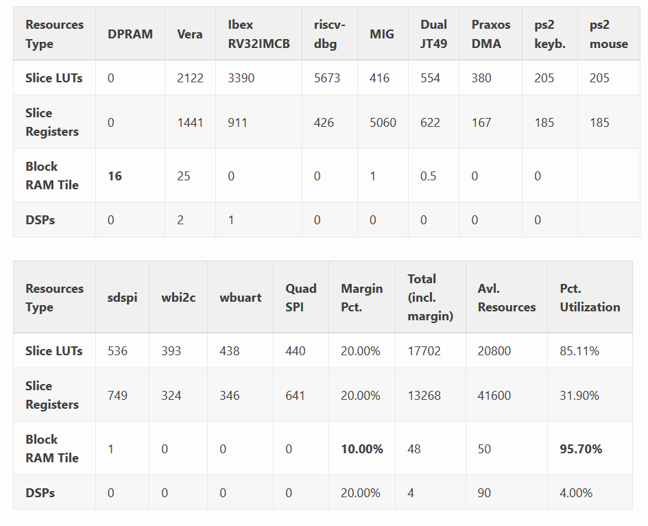
BoxLambda Estimated FPGA Resource Utilization on Arty A7-35T, before adjustment:
Resources Type DPRAM Vera Ibex RV32IMCB MIG Dual JT49 Praxos DMA ps2 keyb. ps2 mouse Slice LUTs 0 2122 3390 5673 554 380 205 205 Slice Registers 0 1441 911 5060 622 167 185 185 Block RAM Tile 32 25 0 0 1 0.5 0 0 DSPs 0 2 1 0 0 0 0 0 Resources Type sdspi wbi2c wbuart Quad SPI Margin Pct. Total (incl. margin) Avl. Resources Pct. Utilization Slice LUTs 536 393 438 440 20.00% 17203 20800 82.71% Slice Registers 749 324 346 641 20.00% 12757 41600 30.67% Block RAM Tile 1 0 0 0 20.00% 71 50 142.80% DSPs 0 0 0 0 20.00% 4 90 4.00% On the Arty A7-35T it’s a tight fit. Actually, the Block RAM doesn’t fit at all. If we reduce the amount of DPRAM to 64KB and reduce the margin on Block RAM to 10%, we can just make it fit:
BoxLambda Estimated FPGA Resource Utilization on Arty A7-35T, after adjustment:
Resources Type DPRAM Vera Ibex RV32IMCB MIG Dual JT49 Praxos DMA ps2 keyb. ps2 mouse Slice LUTs 0 2122 3390 5673 554 380 205 205 Slice Registers 0 1441 911 5060 622 167 185 185 Block RAM Tile 16 25 0 0 1 0.5 0 0 DSPs 0 2 1 0 0 0 0 0 Resources Type sdspi wbi2c wbuart Quad SPI Margin Pct. Total (incl. margin) Avl. Resources Pct. Utilization Slice LUTs 536 393 438 440 20.00% 17203 20800 82.71% Slice Registers 749 324 346 641 20.00% 12757 41600 30.67% Block RAM Tile 1 0 0 0 10.00% 48 50 95.70% DSPs 0 0 0 0 20.00% 4 90 4.00% Slice utilization is also fairly high. This might lead to some routing issues down the line. Still, these numbers are good enough to keep the Arty A7-35T in the running for the time being, at least as a kind of development/prototyping platform. I’m not ready yet to spend the cash on a Nexys A7-100T.
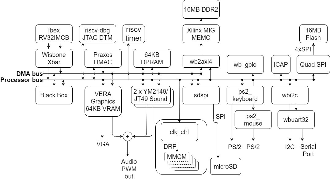
Architecture Diagram Updates
Based on these synthesis results, I settled on the following modifications to the architecture diagrams:
- Ibex processor parameterization RV32IMCB.
- 64KB DPRAM on the Arty A7-35T.
- Replaced the PIT module on the wishbone bus with a Risc-V compliant timer implementation, close to the CPU core.
- Removed the PIC module.
![Nexys Draft Architecture Block Diagram]()
BoxLambda Draft Architecture Block Diagram for Nexys A7-100T.
![Arty Draft Architecture Block Diagram]()
BoxLambda Draft Architecture Block Diagram for Arty A7-35T.
Interesting Links
https://www.linusakesson.net/scene/parallelogram/index.php: Linus Akesson once made an FPGA-based demo. To do that, he created an FPGA-based computer, with a homegrown CPU, shader, and synthesizer. When I grow up, I want to be as cool as Linus Akesson.
-
BoxLambda Architecture, First Draft.
05/22/2022 at 09:44 • 0 commentsIn this post, we organize the key components from the previous posts into an architecture diagram. Along the way, we identify a few new components.
None of what’s shown here is set in stone. The diagrams below contain some speculative pieces and there are quite a few loose ends to tie up as we get further into the project.
The Nexys Configuration
![Nexys Draft Architecture Block Diagram]() BoxLambda Draft Architecture Block Diagram for Nexys A7-100T.
BoxLambda Draft Architecture Block Diagram for Nexys A7-100T.This is a draft architecture diagram showing the Nexys A7-100T configuration. Further down, I’ll show the Arty A7-35T configuration.
Internal RAM
The system is configured with 256KB of Dual-Port RAM (DPRAM) and 128KB of Video RAM (inside the VERA module). The A7-100T has 607KB of Block RAM in total, so more than enough Block RAM should be left over for other purposes, e.g. for the Black Box Module (see below).
The CPU has memory-mapped access to DPRAM. As long as no other Bus Masters are competing for access to the same bus, instructions executing from DPRAM will have a fixed cycle count.
DMA Bus and Processor Bus
The DPRAM is hooked up to two system buses: a DMA bus and a Processor bus. Bus masters (currently only CPU and DMAC) have access to both buses as well, but the intent is that the DMA Controller uses the DMA bus for MEMC<->DPRAM transfers and the CPU uses the processor bus for DPRAM access. This intent is not hardwired into the system, however. The DMA Controller can set up transfers over the processor bus, and the processor can access external memory over the DMA bus. The two system buses are there to give bus masters some flexibility to stay out of each other’s way.
Note that, besides access to external and internal memory, the DMA Controller also has access to VERA, the sound cores, and the SD SPI module via the DMA bus.
Both the Processor Bus and the DMA bus are 32-bit pipelined mode Wishbone buses.
The Interconnect
A bus on a block diagram is just a line connecting blocks. In reality, the Interconnect consists of Cross Bars, Arbiters, Address Decoders, and Bridges. I will follow up with an architecture diagram showing the BoxLambda Interconnect details.
To build the Interconnect, I will make use of the components contributed by the gentlemen below:
- Alexforencich published a collection of components that can be used to build an Interconnect: https://github.com/alexforencich/verilog-wishbone/
- ZipCPU did the same. His components are well-documented, including cross-references with insightful articles on the ZipCPU website: https://github.com/ZipCPU/wb2axip
CPU Configuration
The Ibex CPU configuration is shown as RV32IC, the I and the C indicating Integer and Compressed instruction set, respectively. I would like to include the extensions for integer multiplication and division (M) and bit manipulations (B) into the build as well. Those extensions are going to take up a considerable amount of space, however, and will also have an impact on timing closure. I’m going to defer the decision on those extensions until we have more insight into this project’s FPGA utilization and timing.
Note that there’s no Instruction or Data Cache. Code executes directly from DPRAM or DDR memory. Data access also goes straight to DPRAM or DDR memory.
The Black Box, and other Reconfigurable Partitions
The Black Box Partition is an empty area in the FPGA’s floorplan. This is where you can insert your application-specific logic. Do you need hardware-assisted collision detection for your Bullet-Hell Shoot’em Up game? Put it in the Black Box. A DSP? A CORDIC core? More RAM? As long as it fits the floor plan, you can put it in the Black Box region. The Black Box has bus master and slave ports on both system buses.
Notice that the Black Box sits inside RP_0, Reconfigurable Partition 0. A Reconfigurable Partition is a region on the FPGA where you can dynamically load a Reconfigurable Module (RM) into. Going back to the previous examples, the collision detector, DSP, CORDIC core, or RAM module, would be Reconfigurable Modules. You can live-load one of them into RP_0.
VERA and the two YM2149 cores are also placed into their specific Reconfigurable Partitions (RP_1 resp. RP_2), so you can swap those out for a different graphics and/or sound controller.
The CPU, DMAC, MEMC, and I/O peripheral blocks are all part of the so-called Static Design. These can’t be swapped out for other logic on a live system. Any changes in these blocks require an update of the Full Configuration Bitstream (as opposed to a Partial Configuration Bitstream containing a Reconfigurable Module).
Reconfigurable Modules require a reconfigurable clocking strategy. That’s the role of the Clock Control (clk_ctrl) module. The BoxLambda Clocking Strategy is a topic for a future post.
New Modules
A few new modules popped out of the woodwork:
- PIT, IRQ & GPIO: a placeholder for Programmable Interval Timers, an Interrupt Controller, and General Purpose I/O. I haven’t settled on specific modules yet. To be revisited.
- DFX Controller: The actual loading of a Reconfigurable Module into a Reconfigurable Partition is handled by the DFX Controller. DFX stands for Dynamic Function Exchange which is Xilinx-speak for Partial FPGA Reconfiguration.
- ICAP: Internal Configuration Access Port. This module gives access to the FPGA configuration functionality built into Xilinx FPGAs. We’ll use the ICAP to implement in-system updates of the Full Configuration Bitstream, loaded into the FPGA upon boot-up.
- Quad SPI Flash: This is a module provided by Xilinx, giving access to the Flash Memory device attached through a Quad-SPI bus. The non-volatile Flash Memory will hold the Full Configuration Bitstream(s), System Firmware, and non-volatile system configuration parameters such as keyboard type.
External Memory Access
The Memory Controller is equipped with an AXI4 port. That’s convenient because that’s also what the DFX Controller uses to fetch the Reconfigurable Modules’ bitstreams. To hook up the system buses, we use a Wishbone to AXI bridge. This bridge will introduce additional memory access latency, but that should be acceptable because this path should not be used for latency-critical operations.
Note that the CPU has memory-mapped access to DDR memory and can execute code directly from DDR memory. DDR memory access is not fully deterministic, however. CPU instructions executing from DDR will not have a fixed cycle count.
The Arty Configuration
![Arty Draft Architecture Block Diagram]() BoxLambda Draft Architecture Block Diagram for Arty A7-35T.
BoxLambda Draft Architecture Block Diagram for Arty A7-35T.This is a draft architecture diagram showing the Arty A7-35T configuration.
DFX is not supported on the A7-35T. Neither is the Hierarchical Design Flow. This means we have to stick to a monolithic design. The RTL for all components is combined into one single design, which is synthesized, implemented, and turned into a single bitstream. There is still room for RTL experimentation in this build, but you won’t be able to live-load it. It’s going to require an update of the Full Configuration Bitstream.
The A7-35T FPGA has much less Block RAM than the A7-100T. As a result, the amount of video RAM has been reduced to 64KB, and the amount of DPRAM has been reduced to 128KB.
All other components are the same as in the Nexys Configuration.
Example Software Usage Model
BoxLambda users can make up their minds on how they want to set up this system. Here’s one possible software configuration:
- Deterministic and/or Time-Critical CPU code and data reside in DPRAM.
- Non-Time-Critical code and data reside in DDR memory.
- The CPU accesses DPRAM, DDR memory, and hardware blocks via the Processor Bus.
- DMA activity, if any, passes over the DMA bus.
Loose Ends
This post has briefly introduced several new concepts, and also raises questions on topics not mentioned so far:
- Partial FPGA Reconfiguration (DFX, Reconfigurable Partitions, Reconfigurable Modules).
- Interrupt Handling.
- The System Boot procedure (ICAP).
- In-System Updates (Quad-SPI Flash access).
- Clock Management (clk_ctrl).
- Bus Arbitration.
All of these topics will be further explored in future posts.
Interesting links
https://mega65.org/: BoxLambda is not the only retro-style computer that runs (or rather, will run) on a Nexys A7. Who knows, maybe someday BoxLambda will fit in the super-sexy MEGA65 form factor.
-
Key Components Part 3: DMA and Peripherals.
05/11/2022 at 14:43 • 0 commentsLet’s wrap up the selection of key components for the BoxLambda computer.
DMA
I was on the fence for a while, deciding whether or not I should include a DMA engine in our machine. In a previous post, I said I would use DMA to move data between external and internal memory. However, a DMA Controller is by definition a bus master, and having multiple bus masters (DMAC and CPU) adds significant complexity to the architecture: access to shared buses and slaves, impact on timing, etc. In a system with only one bus master, the CPU, you don’t have to worry about any of that.
Then I snapped out of it and remembered that BoxLambda is intended to be a platform for RTL experimentation. It would be silly to restrict these RTL experiments to bus slave components only. In other words, the BoxLambda architecture is going to have to accommodate bus masters, so we might as well include a DMA Controller.
Some use cases for DMA in the scope of our computer include:
- Moving data between external (DDR) and internal (Block RAM) memory.
- Streaming from memory to the audio DAC.
- Blitting, i.e. copying data into video memory, taking into account the video memory’s organization. For instance, copying a rectangular block of data into a frame buffer requires striding between rows of pixel data. Another example: Bit planes with 1, 2, or 4 bits-per-pixel color depths require barrel shifting when copying data to a specific pixel offset.
I spent many hours online searching for DMA Controllers. I was a bit surprised that there were so few options, so I kept digging. I found ZipCPU’s, FreeCore’s, and Ant Micro’s DMA controllers. The Anti Micro DMAC seemed to be the most interesting option, with two Wishbone ports, pipelined mode, striding support, and support for any byte boundary alignment.
I had this post, with the Ant Micro selection, ready to go. But then I happened across an old post on Reddit where somebody proposed a ‘smart’ DMA concept: a DMAC with a tiny CPU embedded in it. That sounded like a great concept, so I pinged the author to check what became of his idea. In response, the author generously decided to release his code on GitHub! The core is called Praxos. Here is the repository:
https://github.com/esherriff/Praxos
Praxos has tiny CPU with a small amount of program and data memory embedded in the core, allowing you to write microcode specifying the DMA behavior you want: word/non-word alignment, incrementing/decrementing/non-incrementing source and/or destination address, strides between transfers, combining sources, barrel shifting… Maximum flexibility!
It’s not perfect though. Praxos only has one bus master port, an Avalon port at that. It should be doable to slap a standard Wishbone port onto it, but in its current form, I think it won’t be able to take advantage of Wishbone’s pipelined burst mode. That’s unfortunate for a DMAC.
Still, having the option to hack together my own application-specific DMA microcode sounds like a lot of fun. I just have to go with the Praxos option.
Many thanks to esherriff for making his code available!
Storage
I’m going to use ZipCPU’s SD Card Controller in combination with the FatFs software library to mount a FAT filesystem on the SD card:
- SD Card Controller: https://github.com/ZipCPU/sdspi
- FatFs library: http://elm-chan.org/fsw/ff/00index_e.html
The SD Card Controller has a Wishbone slave port.
Keyboard and Mouse
FreeCores has PS/2 keyboard and mouse modules: https://github.com/freecores/ps2
These cores don’t have a Wishbone slave port, so we’re going to have to add that ourselves.
Note that the Nexys A7 has a USB HID host interface for keyboard and mouse which, with the help of clever firmware on a PIC24 microcontroller, presents itself to the FPGA as a PS/2 interface. See the Nexys A7 Reference Manual for more details.
I2C
The I2C interface can be used to hook up a Real-Time Clock PMOD as well as a Wii Nunchuck Adapter.
ZipCPU has an I2C core with a Wishbone port: https://github.com/ZipCPU/wbi2c.
Serial Port
ZipCPU comes to the rescue once again with a UART implementation with a Wishbone interface: https://github.com/ZipCPU/wbuart32
I think that completes the list of Key Components for the time being. More components (e.g. IRQ controller, PIT timers, GPIO) may come into the picture as we get deeper into the architecture or design phase.
Interesting Links
- Amiga HRM, Blitter Section: An in-depth description of Amiga’s Blitter. A good example of how well-designed the Commodore Amiga was.
- www.zipcpu.com: The author of this website, Mr. Gisselquist, is a very experienced FPGA developer. He has contributed a lot of knowledge to the public domain, in the form of verilog code, Blog articles, and tutorials. The Verilog tutorial on this site also serves as a great introduction to formal verification, a frequently recurring topic in the ZipCPU Blog posts.
-
Key Components Part 2: Graphics and Sound Cores.
05/01/2022 at 11:55 • 0 commentsI spent some time researching graphics and sound options for BoxLambda. Here’s what I came up with.
Graphics
If you’re reading this, you must be into the build-your-own-computer thing, which probably means you’re aware of the super cool Commander X16 project. Frank van de Hoef created the very elegant VERA (Video Embedded Retro Adapter) module for the X16. Here’s a high-level specification, taken from the Commander X16 website:
VERA module specifications:
- Video generator featuring:
- Multiple output formats (VGA, NTSC Composite, NTSC S-Video, RGB video) at a fixed resolution of 640x480@60Hz
- Support for 2 layers, both supporting:
- 1/2/4/8 bpp tile and bitmap modes
- Support for up to 128 sprites (with inter-sprite collision detection).
- Embedded video RAM of 128 KB.
- Palette with 256 colors selected from a total range of 4096 colors.
- 16-channel stereo Programmable Sound Generator with multiple waveforms (Pulse, Sawtooth, Triangle, Noise)
- High-quality PCM audio playback from a 4 KB FIFO buffer featuring up to 48kHz 16-bit stereo sound.
- SecureDigital storage.
Other features, not mentioned in the blurb, include:
- Fractional display scaling (scaling lower resolutions up to the 640x480 display resolution).
- Horizontal and Vertical smooth scrolling
Lucky for us, Frank recently released the VERA verilog code under the generous MIT license. You can find the code here:
https://github.com/fvdhoef/vera-module
I’m not particularly interested in VERA’s PSG (Programmable Sound Generator), or the non-VGA output formats, so I might remove those from the build.
The 128KB of video RAM will take a big chunk out of our available Block RAM resources, but it’ll be worth it. We’re getting a lot of bang for our buck.
Note that the VERA is designed as a separate FPGA with a SPI slave interface. Some modifications will be required to integrate it into our SoC.
Xosera
I also considered, but eventually dismissed, Xosera:
https://hackaday.io/project/173731-xosera-fpga-based-retro-video-graphics.
Xosera is a VERA-inspired video controller, but it is being developed independently by Xarc. I like the Amiga-style Copper processor that they added. Unfortunately, Xosera doesn’t have hardware sprites. That’s a showstopper for me. I’ll keep my eye on this project though. It’s an active project and features are still being added.
Sound
A sound core is a perfect candidate for Partial FPGA Reconfiguration. There are a lot of options (Wave-Table synthesis, FM synthesis, PSG…) and a lot of open-source cores available. It would be pretty cool if the software application can just download its synthesizer of choice as part of the program.
Pretty much any core developed by Jotego sounds like a great idea.
Technically, I don’t have to select a sound core. We already have sound through VERA’s PCM audio playback. I’m going to select a sound core anyway because I like retro sounds and I’d like to mess around a bit with one of the old-school PSG chips.
I think I’ll go for a dual YM2149, one for music, one for sound FX, in a game context. The YM2149 was the Atari ST’s sound chip, so we’ll have a large music and sound FX archive at our disposal. Jotego developed an FPGA clone of the YM2149, the JT49:
https://github.com/jotego/jt49
Why not VERA PSG?
The only reason I’m not going for VERA PSG is that, as of yet, very little music has been written for it. I’m sure it is a perfectly adequate PSG implementation.
Why not SID?
The SID chip is partially analog, making it much harder to emulate correctly on an FPGA. Also, while I like SID, I’ve probably heard enough SID music to last me a lifetime. I’m currently more interested in finding out what other retro sound chips have to offer.
Interesting Links
- https://misterfpga.org/ : Jotego is one of the key developers behind the MiSTer FGPA project.
- https://www.youtube.com/watch?v=u5Mi3FkZgFI : a compilation of some excellent YM2149 music made for the Atari ST by genius composer Scavenger (Joris de Man).
- https://en.wikipedia.org/wiki/List_of_sound_chips : A list of sound chips
- Video generator featuring:
-
Key Components Part 1: Bus, Microprocessor and Memory Controller.
04/23/2022 at 17:08 • 0 commentsIn the previous post, we discussed top-level requirements. Now we drill down one level, identify key components and apply our requirements to them. We also look around for existing cores or applicable specs that might fit the bill.
The Bus
The Bus, or interconnect, is the fabric stitching together the SoC internal components. For this project, the two most relevant SoC internal bus specifications are ARM’s AXI bus and the Open-Source Wishbone bus.
AXI is very powerful, very popular, and very complex. It scales up well to very big SoCs. However, I don’t think it scales down very well to simple SoCs, such as BoxLambda, where low latency and low complexity are more important than high bandwidth and scalability. Hence, for this project, I’m electing to go with Wishbone.
We’ll be using the Wishbone B4 specification.
Sticking to a well-defined internal bus specification certainly helps to meet the Modular Architecture Requirement. Whether we can also accommodate Partial FPGA Reconfiguration using a Wishbone Interconnect remains to be seen.
The Processor
Processor Word Size
Typical processor word sizes are 8-bit, 16-bit, 32-bit, and 64-bit. Which word size is the best fit for Boxlambda?
- 8-bit: A good word size.
- Pros:
- An 8-bit word (i.e. a byte) is a good natural fit for a pixel value, an ASCII character code, or small integer values.
- 8-bit processors, their programs, and their data are very compact.
- 8-bit processors side-step some of the alignment issues seen with larger word sizes.
- Cons:
- An 8-bit word is too small to conveniently hold the values you need in a typical program - think calculations and table indices.
- Toolchain support for higher-level languages is limited.
- Pros:
- 16-bit: A clumsy compromise between 8-bit and 32-bits. Made sense when 32-bit processors were not readily available yet. Now, not so much.
- 32-bit: Another good word size.
- Pros: 32-bit words can hold most real-world numbers and cover a huge address space. 32-bit machines generally have good toolchain support.
- Cons: Much bigger than its 8-bit counterpart, in terms of FPGA real estate, program size as well as data size.
- 64-bit: A big and clunky word size, way too big to handle conveniently, intended for specialized use cases that don’t fit this project.
I’ve decided to go for a 32-bit processor. A 32-bit processor (and associated on-chip memory) will take a bigger chunk out of our FPGA real estate, but I think it’s worth it. I like the convenience of 32-bit registers, and a 32-bit processor may come with a regular GCC toolchain.
Processor Features
Next to a 32-bit word size, we’re looking for the following features for our microprocessor:
- Ease of programming, meaning:
- Easy and well-documented Instruction Set Architectures (ISA). We want to be able to program the machine at assembly language level.
- Shallow Pipeline: It is relatively easy to reason about the behavior of a processor with a two-stage pipeline. It is not very easy to reason about the behavior of a processor with a six-stage pipeline.
- Good toolchain support, such as GCC, so we can build a software ecosystem for our machine.
- An accessible and well-documented implementation.
- Has to fit our FPGA, with enough space to fit the other components.
With all that in mind, I think RISC-V is a great option.
- Great ISA, building on lessons learned from previous popular processor architectures.
- 32-bit support.
- GCC toolchain support.
- Open-Source.
- Well-documented.
- Very fashionable. Let’s ride that wave :-)
There are a lot of RISC-V implementations to choose from. The Ibex project seems like a good choice:
- 32-bit RISC-V.
- Hig-quality, well-documented implementation.
- SystemVerilog based. My preferred HDL.
- Supports a small two-stage pipeline parameterization.
- Very active project.
The Memory Controller
SDRAM memory access is pretty complicated. Memory access requests get queued in the memory controller, scheduled, and turned into a sequence of commands that vary in execution time depending on the previous memory locations that were recently accessed.
There exists a class of memory controllers, called Static Memory Controllers, that absorb these complexities and by design create a fixed schedule for a fixed use case, resulting in very predictable behavior. Static Memory Controllers are far off the beaten path, however. Dynamic Memory Controllers are more common. Dynamic Memory Controllers can handle a variety of use cases with good performance on average. Unfortunately, they sacrifice predictability to achieve this flexibility.
Ideally, we would use an accessible, well-documented, open-source, static memory controller design. Unfortunately, I can’t find one. Rolling our own is not an option either. Doing so would require so much specific know-how, that it would kill this project. Pragmatically, our best option is to use Xilinx’s Memory Interface Generator (MIG) with the Arty A7 (or Nexys A7) parameters as published by Diligent.
The Xilinx memory controller falls squarely into the Dynamic Memory Controller class. How do we fit this into a platform that requires deterministic behavior? I think the best approach is to use a DMA engine to transfer data between SDRAM and on-chip memory. Fixed memory access latency to on-chip memory (from any bus master that requires it) can be guaranteed using an arbiter. We’ll revisit this topic when we’re discussing Boxlambda’s architecture.
Interesting Links
- 8-bit: A good word size.
-
Requirements Analysis
04/23/2022 at 17:08 • 0 commentsEvery new project starts with an empty document, a blank sheet. It’s a unique moment where you have complete freedom. As soon as you put something down in the document, you’ve made a choice and your options become limited. With each subsequent choice, you limit yourself more, until there are no more choices to make, at which point the project is complete. So, in a way, this post, along with the previous one, are the two most important posts of the whole project. We’re making our first choices, setting the direction of this project.
Let’s go over the project’s goals/requirements and clarify a bit what they mean.
Simplicity
Simplicity will be a strong guideline when making design choices. For instance, it may mean that we decide against a popular-but-complex processor in favor of a more obscure-but-simple processor.
It is hard to make something simple. The Simplicity requirement will make system design harder, not easier. For a case in point, see below.
Deterministic Behavior
Designing a deterministic system is more complex than designing a system that allows some slack in the completion of operations. However, once such a system is in place, it becomes much easier to reason about it and design applications on top of it, especially applications with real-time requirements. For instance, it would be pretty cool if the system is designed so that racing-the-beam becomes possible, i.e. time actions within an application’s main loop so that they take place on a specific screen scan line and a specific column on that scan line. Think Commodore 64 split raster bars and sprite multiplexing.
Note that deterministic behavior must be guaranteed only when required by the application. Less deterministic operations are perfectly acceptable when the application does not require full deterministic behavior. E.g. a deterministic application runs from Block RAM with known, fixed memory access latency, while a non-deterministic application may run from bursty external memory.
One consequence of the Deterministic Behavior requirement is that bus arbitration should be done using fixed time slots to be able to guarantee fixed timing, latency, and bandwidth to each bus master.
Single User / Single Tasking OS
We won’t be running Linux or any other multitasking OS for that matter. The platform will only run one application at a time and that application will be fully in charge of the entire system.
A Single User / Single Tasking OS will provide the following services:
-
A console CLI shell allowing user and scripted access to:
- navigate the file system
- load/save software images to/from memory
- copy/move/delete files
- execute (transfer control to) applications in memory, optionally passing in command-line arguments
- peeking and poking into memory
- File System I/O kernel routines
- Console I/O kernel routines: Input from a physically attached keyboard, output to a physically attached screen.
- UART I/O kernel routines
- Discovery and enumeration of hardware components. See Modular Architecture below.
Not Boot-to-Basic
I don’t want to be pinned down to, or give preference to, any particular interpreted language, so we’re not going going to Boot-to-Basic. We’re not going for full-retro boot-to-Basic.
I would like to allow open support for multiple interpreted languages by letting the application image indicate in which language it’s written, e.g. by specifying on the first line the path to the interpreter to use, as commonly used in Linux scripting: #!/usr/bin/python, #!/usr/bin/ulisp, …
It should also be possible to directly execute binary images of course.
Modular Architecture
I imagine a reference configuration to which hardware components can be added or from which components can be removed. Applications should be able to discover, with the help of the OS, whether a certain component is present or not.
Partial FPGA Reconfiguration
It would be very cool if a hardware component can be incrementally loaded into the FPGA, using Xilinx’ DFX (Dynamic Function eXchange) feature. This would allow applications to be packaged along with specific hardware components (e.g. accelerators or peripherals) on which they depend.
I’m considering this feature a stretch goal for the project.
Target Hardware and Peripherals
I currently have an Arty A7 35T, with the following PMODs for peripherals:
- Pmod MicroSD: microSD Card Slot
- Pmod PS2: Keyboard/mouse connector
- Pmod AMP2: Audio Amplifier
- Pmod VGA: Video Graphics Array
- Wii Nunchuck Adapter
I suspect that over time the project will outgrow this setup and I might move up to the Nexys A7-100T, also from Diligent. Compared to the Arty A7 35T, Nexys A7-100T has:
- A bigger FPGA: More logic slices and more Block RAM.
- Onboard microSD card connector
- Onboard PWM audio output connector
- Onboard PDM microphone connector
- USB HID for keyboard and mouse, with a clever adapter so keyboard and mouse present themselves to the FPGA as PS/2 devices.
- VGA connector
Interesting Links
https://www.linusakesson.net/programming/poems-for-bugs : A great talk from Linus Akesson about C64 coding, explaining why to this day people are still compelled to develop games and demos for this wonderful machine.
-
-
Introducing the BoxLambda Project.
04/23/2022 at 17:06 • 0 commentsAlright, this is it. We’re live. I’m starting a project called BoxLambda. Here’s the run-down, copied verbatim from the README.md:
BoxLambda is an open-source project with the goal of creating a retro-style FPGA-based microcomputer. The microcomputer serves as a platform for software and RTL experimentation.
BoxLambda is a software-hardware cross-over project. The plan is to provide room for experimentation both on the FPGA RTL side and on the software side.
Key Goals
- Create a sandbox for experimenting with software and (FPGA) HW.
- Simplicity: It should be easy to jump in and do something: create, hack, tinker.
- It should be doable for a single person to develop a good understanding of the entire system, software and hardware.
- Deterministic Behavior: By design, it should be clear how long an operation, be it an instruction or a DMA transfer, is going to take.
- Single User/Single Tasking OS booting to a console shell.
- Create a Modular Architecture allowing for a mix-and-match of software and hardware components.
- Support for partial FPGA reconfiguration.
- Simplicity: It should be easy to jump in and do something: create, hack, tinker.
- Target Hardware is Digilent’s Arty-A7 and/or the Nexys-A7.
- The computer should support the following peripherals:
- Keyboard
- Mouse (optional)
- Joystick (optional)
- Serial port
- SD card storage
- VGA Display
- Audio output
- Sound and graphics should be sufficient to support retro-style 2D gameplay.
You can find the source code for BoxLambda on GitHub: https://github.com/epsilon537/boxlambda/.
Why?
Does the world need another retro-style computer? Probably not, but I do. I’m a software engineer and I’ve been studying FPGA development for about a year now, specifically for this project.
It’s an ambitious project and at least half of it (the FPGA half) is in a realm with which I have very little experience. I don’t know if the project will succeed. Maybe I’m too ambitious and too naive. We’ll see. This Blog will document the journey.
What’s up with that name, BoxLambda?
“Box”, as in, a physical box. “Lambda”, as in, an anonymous function, a software concept. It’s an attempt to convey that this project is both about hardware and software. Microsoft would have been a good fit too, but the name was taken.
Interesting Links
https://www.commanderx16.com : The Commander X16 is the 8-Bit Guy’s dream computer. This is the project that got me dreaming. I want to build a computer like this, but not exactly like this. I want to build my own.
OK, that’s enough for an introductory post I think. See you in the next one!
- Create a sandbox for experimenting with software and (FPGA) HW.
BoxLambda
A retro-style FPGA-based microcomputer. The microcomputer serves as a platform for software and RTL experimentation.
 Iterative Design Spiral
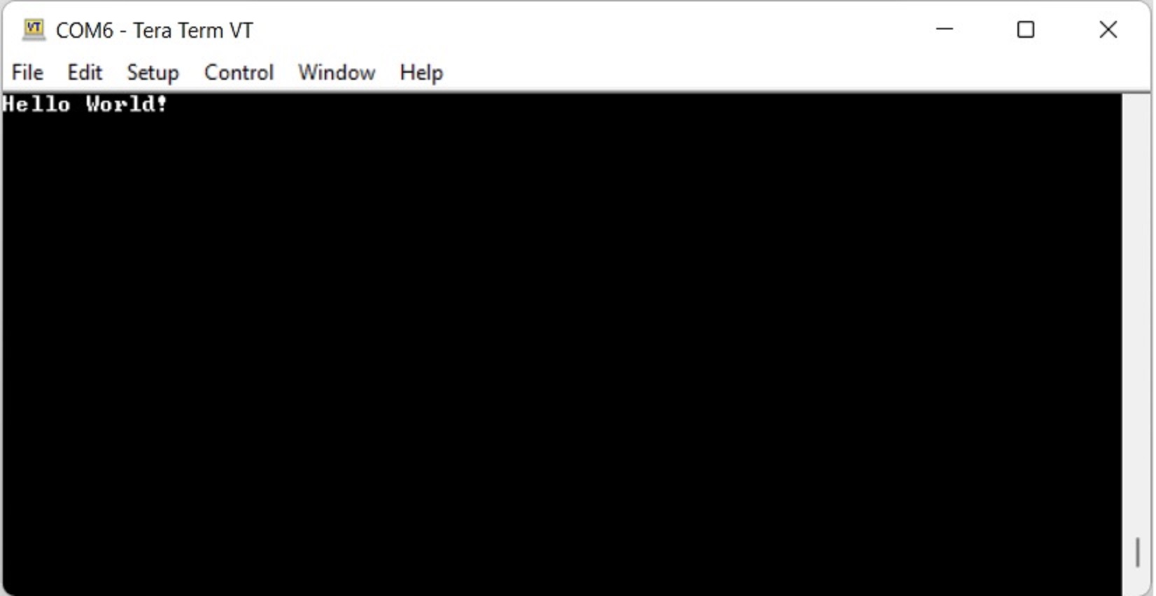 Hello World! from ibex_wb on Arty A7-35T
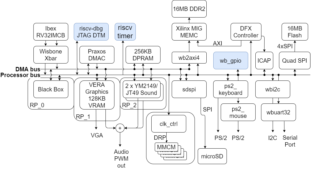 BoxLambda Architecture Block Diagram (Nexys version)
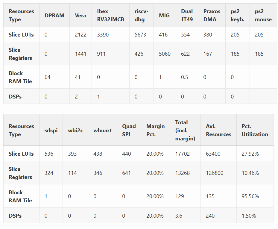
 Connecting to Target from Vivado on WSL
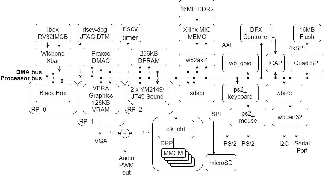
 BoxLambda Draft Architecture Block Diagram for Nexys A7-100T.
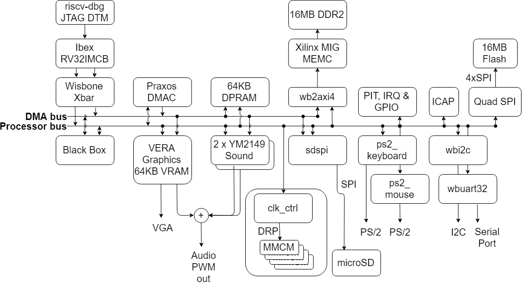 BoxLambda Draft Architecture Block Diagram for Arty A7-35T.