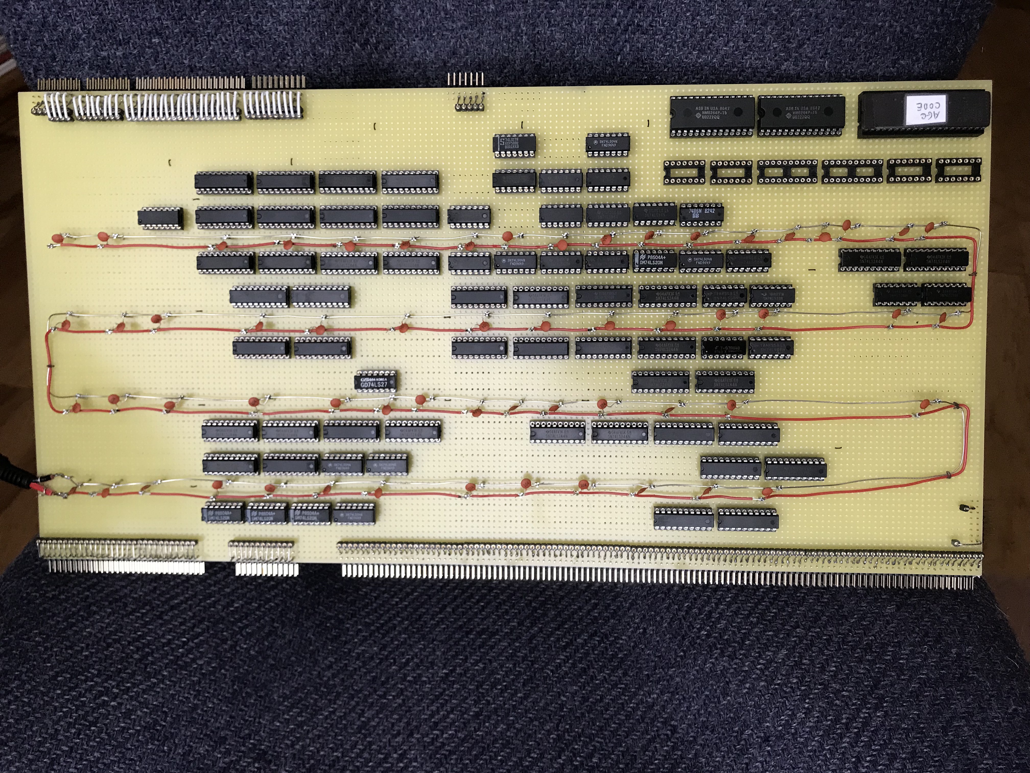
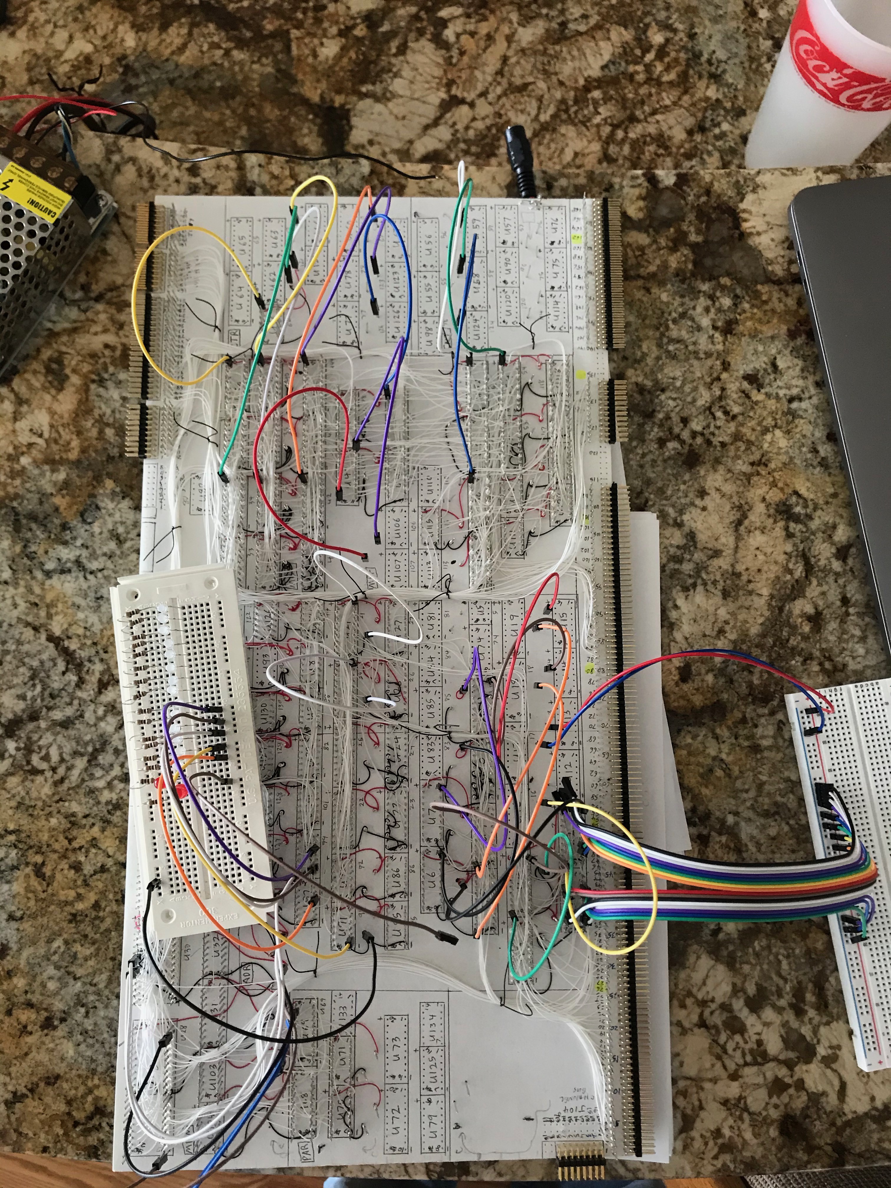
This is where I started. I added the code EPROM and RAM, then started adding various access registers before I became overwhelmed using just my simple 16-bit register viewed. I realized I needed the Display sub-system so I switched gears and have been working on that. Here are some pictures of where I am to date.


Even though I have the AGC Code EPROM plugged in, I will probably start with some simpler test programs I have created to test various commands that never seemed to come up in the AGC code. Some of that code contains the more complicated multiply and divide instructions. The documentation has good test case scenarios that I used to make sure they are working.
Here are some design notes that help understand the schematics.
Erasable/Fixed Memory: This module contains a single EPROM chip that contain the code which was generated using the modified assembler. This is a 16-bit data by 16-bit address chip that can handle all the code in the Luminary 099 program. There are also two RAM chips that implement the erasable memory.
The single 16-bit EPROM brings some simplification from a chip count, however it is more complicated from an implementation standpoint. The data lines are a bit reversed from what you might expect. The bytes are reversed and I did not attempt to change this as it is easier to read and verify in this configuration. From a hardware perspective, it is a simple matter to switch the byte's data lines. If the address is 0 then the first data word is 1687 hex. Given this, the data lines are as follows.
1 = D7 – D4
6 = D3 – D0
8 = D15 – D12
7 = D11 – D8
The address lines are as you would expect when dealing with the EPROM. For instance, address 4000 octal equals 800 hex which will give a data value of 0004 hex. The S-Record format is what is a bit strange. The data is defined a byte at a time. To see this data value in the S-Record file, double the address value. In the case of 4000, double 800 hex gives a value of 1000 hex. Looking at the S-Record values at this location you will see 00 04 38 2c.
Memory Buffer: This module encapsulates the G register. All data in and out of memory go through this register. The shifting when writing to addresses 20, 21, 22 and 23 occur in this module. Data arrives via the Write Bus and Direct Write Bus. The data read from fixed memory is checked for specific values; all zeros or GMZ, EQ3, EQ4 and EQ6. The EQ pulses check for the TC instructions that translate into the RELINT, INHINT and EXTEND instructions.
The determination of the four specific G register values results are straight forward except the combination of the CYR and SR. All the bits are the same except bits 14, 15 & 16. The table below shows the values.
| Bit | W20 | W21 | Equation |
| 14 | B15 | B16 | (!W21 * B16) + (!W20 * B15) |
| 15 | 1 | 0 | W21 |
| 16 | 0 | B16 | (!W21 * B16) |
Parity: This module in Block I was driven by control pulses within the Control Pulse Matrix. In Block II they realized you always generate parity when writing to memory and test parity when reading from memory. I kept the control pulses as internal pulses to drive this functionality. I chose to implement parity for the erasable ROM memory, but not for the fixed memory. It would be easy enough to implement this if you wanted to.
This functionality is implemented using two parity generator chips. This module contains the P register and PALM (parity alarm) single bit register.
Interrupts: This module implements three of the interrupts; the keyboard interrupt along with TIME3 and TIME4. The inhibit interrupts is also implemented in this module. A RPCell register maintains which interrupt has occurred. When an interrupt is processed, this module converts the specific interrupt into the memory address of the code's interrupt jump table. The address equals 04000 + RUPT # << 2. The addresses are (in octal).
4014 = RUPT3(TIME3)
4020 = RUPT4 (TIME4)
4024 = RUPT5 (KBD
Counters: This module implements four of the counters. The implemented counters and their octal addresses are as follows.
TIME2 = 24
TIME1 = 25
TIME3 = 26
TIME4 = 27
When counters TIME3 and TIME4 overflow, they generate an interrupt. When counter TIME1 overflows, it increments the TIME2 counter. The TIME2 counter should never overflow.
A counter address is generated when asked for by the RSCT control pulse. This is the address of the counter to increment (shown above).
Discussions
Become a Hackaday.io Member
Create an account to leave a comment. Already have an account? Log In.