-
Video system
08/22/2023 at 18:51 • 0 commentsThe Isetta video system will now be described.
GENERAL
The generated signal is a VGA signal with a maximum resolution of 640 x 480 pixels.
The timing is:
25.175 master clock
approx. 40nS per pixel (for 640 pixels/line)
approx. 32uS scanline
A whole scanline has a width of 800 pixels (only 640 pixels used)
A whole frame has a height of 525 scanlines (480 scanlines used).
Exact values can be found here.The isetta can work with maximum or reduced horizontal resolutions:
- 40nS per pixel (for 640 pixels per line)
- 80nS per pixel (for 320 pixels per line)
- 160nS per pixel (for 160 pixels per line)
In the vertical direction, scanlines can be repeated (to keep the pixels almost square, also when a lower horizontal resolution is used), giving:
- 480 lines, or
- 240 lines (480 divided by 2), or
- 120 lines (480 divided by 4)
There are 64 colors (but the color can not be freely chosen for every pixel).
HARDWARE PRINCIPLE
The Isetta processor runs with a cycle of 160nS (6.25 MHz). The video output is directly generated by the processor, so during every instruction, one or more pixels must be generated:
- 1 pixel/instruction (for 160 pixels per line)
- 2 pixels/instruction (for 320 pixels per line)
- 4 pixels/instruction (for 680 pixels per line)
Isetta contains a hardware timer that triggers an interrupt at the beginning of every scanline. At the beginning of the visual part of the screen, this interrupt transfers control to the microcode that has the video instructions to give screen output. It can also initiate the generation of the frame sync pulse (the line sync pulse is generated by the hardware timer). If the interrupt is outside the visible area, the interrupt code will only increment the line counter, and return to the interrupted program almost immediately.
A video instruction will get a single byte from the RAM, and gets color information, pixel information, and sometimes control information (flags) from that byte.
The microinstruction fetches this byte from the indicated RAM location.
The RAM is normally addressed with the (PC++) mode (Of course this requires that the PC that was used in the Z80 or 6502 program was saved when the interrupt is entered).The color information is 6 bits. The instruction can store the color in register T (foreground color) or in register A (background color).
Information about a pixel is only 1 bit. If that bit is 1, the color of the pixel comes from register A. If the bit is 0, the color comes from register T.
We now come to the basic byte formats that are used for the video system.
- Color definition:
Byte format: -cccccc-
The 6 color bits 'cccccc' can be transferred to the T (Foreground, FG) or A (Background, BG) register.
- 320 pixels/line :
Byte format: a------b
Two pixel bits 'ab' select the two pixels to be used in 320 pixels/line mode. These pixels are placed in the 4-bit 'pixel register' as 'bbaa'. The pixel register is loaded at every instruction, so the information is only available in the next cycle.
- 160 pixels/line :
This format is the same as the 320 pixels/line format, but in this case the bits a and b simply have the same value.
- 640 pixels/line :
Byte format for 4 pixels: --pppp--
Four pixel bits 'pppp' select four pixels to be used in the 640 pixels/line mode. These pixels are transferred to the DPH register, and the output of this register is connected to a multiplexer that selects the correct pixel to be displayed. The 'pppp' bits are in bit5, bit4, bit3 and bit2 of the byte. The pixel register is connected to other inputs of the same multiplexer.Byte format for 2 pixels: ab-----1
This 2-pixel byte must be loaded with a SHL (shift left) instruction, while shifting a '1' into bit0. That will put the bits in the 4-bit pixel register as '11ab'. The '11' section defines background color (in register A).
- Select pixel register or DPH register:
One of the bits in the microinstruction ( ctl_reg1 ) determines if the pixel information comes from the 4-bit pixel register or from the four '--pppp--' values in the DPH register. This is done in the cycle that follows the instruction that loaded the byte.
Note that there can be combinations of bytes:
- Color can be combined with 320 pixels/line, to 'accccccb'
- Color can be combined with 640 pixels/line, to 'abccccc1' (only 5 color bits here)
- For 640 pixels/line, 4 pixel and 2 pixel format can be combined to ab-pppp1 (defining 6 pixels)
APPLICATION OF THE VIDEO INSTRUCTIONS
At the start of the visible area, the processor should set the 'blank' signal (in the output port) to zero. This enables the video output, and selects the A or T register on the operand bus, based upon the pixel value (while this selection is normally determined by the microinstruction). During video output, the microinstruction can select A on the operand bus to force the color to background.
At the start of a video line, a table will be accessed that has the relevant information for this line:
- The start address of the video data. The SW can manipulate this address, e.g. having the next line point to the same data address, for 240 lines or 120 lines mode. The video data address will be placed in the PC.
- A pointer to the video instructions to use, that will determine the actual video mode for this line. So the video mode can be different for each line.
- A default value for the FG and BG color (for 640 pixels/line mode).
- For 40-char text mode, a byte that contains the row address of the character generator.
320-pixel/line Graphic mode
A normal 320-pixel/line can alternate between loading a new FG color and loading a new BG color. Every instruction will also provide the two 'bbaa' bits to the pixel register.
A <- (PC++) // load BG color and ab bits, display 'bbaa' in next cycle
T <- (PC++) // load FG color and ab bits, display 'bbaa' in next cycle
A <- (PC++)
T <- (PC++)
A <- (PC++)
T <- (PC++)
etc
640-pixel/line 2-color graphic mode
A 640-pixel/line can be used for 2-color graphic output. The FG and BG colors must already be present in the A and T registers:
DPH <- (PC++) // provide four --pppp-- bits
DPH <- (PC++) // provide next four --pppp-- bits
DPH <- (PC++) // provide next four --pppp-- bits
DPH <- (PC++) // provide next four --pppp-- bits
etc
40-char/line text mode
The 320-pixel/line graphic mode can also be used to display text.
But it is also possible to use a character definition bitmap somewhere in memory. We spread the definition of a single row (6 pixels) over 3 memory banks. These locations also contain the foreground color of the character.
The first instruction places the character code in DPL. The DPH register is already set to the correct row of the character (done before the start of the line). The video data can be the same for each row in a character. If we start the video data at address 0x0400, the behaviour will be similar to the text mode of the Commodore 64: Write an ASCII value in the range 0x0400-0x7FF and the character will appear on the screen.
dpl <- (pc++)  // char code.  DPH is set at beginning of line. Suppress pixels(with A/T select)
T <- (dph/dpl,bank1)  // pixels/color accccccb  (color specified in bitmap)
T <- (dph/dpl,bank2)  // pixels/color accccccb
T <- (dph/dpl,bank3)  // pixels/color accccccb
etc
2-color 80-char/line text mode
We use essentially the graphic mode for this. The 640 pixel/line mode will probably be used with 400 or 480 lines per screen, so this will take a lot of memory (But we can use a memory bank outside the normal 64kB area).
There is way to reduce the memory usage when text is used, by providing 6 pixels in a byte, in the ab-pppp1 format. A first instruction will load the byte and display the '11ab' bits in the next cycle. The next instruction will display the 'pppp' bits in its next cycle.
So the character is 8 pixels wide, but the first two pixels are '1' (background).
DPH <- (PC++)   // load ab-pppp1 and display 11ab in next cycle
NOP             // display pppp in next cycle
DPH <- (PC++)   // load ab-pppp1 and display 11ab in next cycle
NOP             // display pppp in next cycle
etc
Multicolor 80-char/line text mode
In this mode, the first instruction loads 2 pixels and a 5-bit color. The next instruction loads 4 pixels, together this are 6 pixels for the character. This repeats for the next characters. So every character can have a different color.
T <- shl(pc++)  // abccccc1, 2 pixels, shift, pixels 11ab, color ccccc1
DPH <- (pc++)   //  --pp pp--, load 4 pixels
T <- shl(pc++)
DPH <- (pc++)
etc
[ Edit 230830 The definition of the byte formats, and the application section, have changed. This log was made up-to-date. ]
-
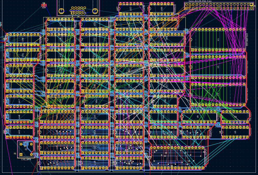
Started KiCad layout
08/06/2023 at 10:49 • 2 commentsThis is the first project where I use KiCad (version 7.0.2).
Schematic entry was quite smooth, but with the pcb layout I experienced some problems. It was difficult to arrange the components on a 0.1" grid. And since I do everything on a 0.1" or 0.05" grid, it is annoying that KiCad displays things like cursor position only in millimeters. [ Edit. You can set this to inches, see comments ].
Routing is not very difficult, but I miss certain functions. But it is possible that I do not yet know all commands for routing.
But don't get me wrong, I think the KiCad developers did a great job !
Here is the current state (you can click on the picture to get more detail) :
![]()
The lower part of the pcb is routed. For the rats nest I use several colors:
- red, VCC
- blue, GND
- light blue, databus
- green, address bus, micro-address bus, internal ALU signals
- magenta, microcode bus
- yellow, operand bus
- orange, result bus
- white, several control signals
This is far from finished, especially I/O components must still be added.
-
Update
07/21/2023 at 21:15 • 2 commentsIn the past months i've been working on the hardware design and the microcode.
The number of required IC's got too high in my opinion, so some hardware was removed, every removal costing some effort to implement the removed instruction in microcode. I removed the following items:
- The 74ac151 that calculated the V flag. Now, the two bit-7 adder inputs and the bit-7 adder output, needed to calculate the V flag, are connected to an input port (that has some unused inputs), and the value is saved after every addition/subtraction (or 6502 BIT instruction). When the V flag is tested, it is first calculated (by using the 3 bits to compose an opcode, and executing that opcode).
- The zero-calculation. This was composed of three 3-input NOR gates (74F27) and a 3-input AND gate (74ac11). The other gates in the 74ac11 could not be used somewhere else, so this saves 2 IC's. After a ALU operation, the result byte is now saved to a (memory-based) register called reg_z. When the Z flag is tested (for a BEQ or BNE instruction), an 0xFF value is added to this register (same as decrementing), and when a carry occurs, the value was non-zero. There also was a physical flag Z and a upd_z microcode bit that indicated that this flag had to be updated. Both are not needed any more, and the upd_z frees a microcode bit that will be used to double the amount of available (memory-resident) registers. But it costs one extra cycle at every instruction that updates the Z flag, and one extra cycle when the Z flag is tested.
- The shift-right multiplexers (2 x 74hc157) were removed. Shift-right is now done with a table in RAM (outside normal 64K section). After reset, some microcode constructs this table.
- There was a special 8-bit buffer to put a byte of microcode on the databus. It was intended for special microinstructions that could place this byte in RAM (at an auto-incrementing pc++ position). This would be convenient for moving boot-code to RAM directly after reset. But this can also be done without this buffer, costing one extra microinstruction per transferred byte, and some microcode to organize this.
- It was intended that the video section would have it's own RAM, such that video can be generated while the cpu is doing it's own thing. This will now be an option (additional pcb, called 'performance option' ), and the on-board video is bit-banged by the cpu ( 'economy version' ). It saves around 8 or 9 IC's.
Of course I've been thinking about the video generation. The on-board economy version will have a 6-bit color value in both the A and T register. A multiplexer will select which color is connected to the output. There can be a few video modes, and the video mode can be different for each line. The basic video modes are:
- 160 pixels/line. In every 160nS cycle, the A register will be filled with a new 6-bit color, providing 160 pixels per line, of 64 colors each. (it is just a special case of the 320 pixel/line mode).
- 320 pixels/line. In every 160nS cycle, the A register will get a new 6-bit color. The remaining two bits determine the color of the two 80nS pixels that will be displayed in this cycle. Each pixel is either the foreground color from the A register, or the background color from the T register.
- 80 column text mode. In an 'odd' 160nS cycle, 7 bits will be read, 4 bits will be 40nS pixels in the odd cycle, and 3 bits are 40nS pixels in the next ('even') 160nS cycle. The 4th pixel in this next cycle will be background color (blank pixel between characters). Again, each pixel is either the foreground color from the A register, or the background color from the T register. Since only 7 bits of the byte are used, there is one spare bit that indicates that a new foreground and background color will be loaded in the next two 160nS cycles (while displaying a space character).
During the verical blanking time, the cpu will be executing instructions. At the end of every line, it will get an interrupt, that counts the lines, organizes the vertical sync pulse, and checks if a line of video pixels must be written. (There is a hardware counter that generates the line interrupt).
This week I was working on the interrupt response time. I measured this time with the emulator while running the Apple Basic or TRS80 basic, and the maximum delay between two tests of the interrupt signal was quite long (more than 40 cycles). While most instructions checked the interrupt (by moving the IRQ signal to the F flag, and then jumping to the interrupt routine at the end of an instruction when F is active), there were a few instructions (like conditional jumps) that needed F for another purpose, or that had no opportunity to move the IRQ to the F flag (because moving to F flag does not go together with an ALU operation like ADD, SUB, AND, INC).
The last problem was solved by defining that, at the end of every instruction, the F flag should represent the IRQ state. So the microcode was changed to accomplish this.
The next thing to improve the response time, is to test the interrupt state not only at the end of an instruction, but also in the middle or at the beginning of an instruction (especially for instructions that have a lot of cycles). In this case, a special interrupt entry will be jumped to, that sets the PC one or two bytes back, so the same instruction will be repeated when the interrupt has ended. Of course, the interrupted instruction must not already have done actions that will cause misery when they are repeated.To be continued...
-
Another interesting BASIC to test the 8080 instructions
05/23/2023 at 18:52 • 1 commentSince the Isetta supports instructions of the Z80 processor, it also supports the famous 8080 processor, because the Z80 has the 8080 instruction set as a basis. The 8080 is interesting because it is the grandfather of almost all INTEL CPU's for personal computers of the past 40 years.
One of the very first personal computers was the Altair 8800 from the company MITS. It was built around the 8080 processor. Bill Gates, Paul Allen and Monte Davidoff created a BASIC interpreter for this computer, the Altair BASIC. It was called a 4KByte BASIC. But the actual program was smaller than 4K, because 4K was all memory that the Altair had ! There were only 790 bytes free for user programs ! Altair BASIC was the very first product of Microsoft !
So I used this Altair BASIC to test the 8080 instructions on the Javascript emulator of the Isetta processor. I found an Annotated disassembly and a binary version. And I really needed the disassembly, to understand a little of the program.
Subtract and compare
After the first tests, I found that for the 8080/Z80, the carry flag behaviour for the subtract and compare instructions is inverted w.r.t. the behaviour in the 6502. I created a new microinstruction that complements the carry flag for the 8080/Z80. In several situations, it can be executed at the same time as another microinstruction.
Parity flag
Altair Basic has a FCompare at 0A4C that compares two floating point numbers. It returns
one of the following values:- 0x00 for zero
- 0x01 for greater than zero
- 0xFF for less than zero
That's very logical. Now you can simply test the sign flag or zero flag to jump according to the result.
But in two instances, at 0B63 and 0C03, it is followed by a JP PO (jump on parity odd) instruction, that will jump if the result is greater than zero (as 0x01 is the only one of these three values that has an odd number of '1' bits in the byte)
On the 8080, (almost ?) all arithmetic and logic instructions that act on the accumulator will
set the P flag according to the parity.But on the Z80, the parity flag behaviour is different. Logic instructions will set the flag according to the parity, but the arithmetic instructions will set the flag when there is an overflow. And indeed, it has been reported on the Internet that the Altair Basic will not work on a replica Altair that has a Z80 processor instead of the 8080 in the original Altair.
So, although it is widely believed that the Z80 can run all programs intended for the 8080, this is not true because the behaviour of the P/V flag is different.
And on the Isetta it is also a problem because parity is not implemented at all.
The parity flag is tested with JP PO on only two occasions, at 0B66 and 0C04. Both instances are preceded by a call to FCompare at 0A4C. I replaced the calls to FCompare by a new subroutine, that does the following:
- Call the FCompare function at 0AC4
- Return if result is non-zero
- Save Accumulator
- Load Accumulator with 0xFF, and OR A to set the sign flag
- Restore Accumulator and return
Both JP PO instructions are now replaced by JP P (jump if positive). The parity flag is not needed any more (at least not for this BASIC).
A nasty bug
Strange thing were going on. The display of numbers displayed the first digit as a letter. And with another test program (TRS-80 Basic), identifiers were not recognized. After a few days, I found out that the carry flag was not cleared after an XOR A,A instruction. The microcode seemed ok, it said the carry was written (and at the same time a load operation was done). But for the carry-complement (for subtract and compare) I changed the behaviour such that writing the carry while doing a load resulted in a complement-carry ! Sometimes it is difficult to program your own contraptions.
Other changes to the BASIC
The code at the following positions was changed for character output and keyboard input:
- The code at 0377 that handles character output
- The code at 0382 that handles keyboard input
Another thing was, that this basic is full of self-modifying code. I found that when the program is initializing, it somehow seems to find out at which I/O ports the character I/O is, and writes the I/O addresses directly into the instructions that do the I/O ! So these initialisation code was changed to NOP's.
The initialization code is at the end of the program. After initialization, this code is overwritten by the user's program.
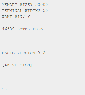
After all is done, we see the following:
![]()
At startup, the user must tell what the memory size is, and how many characters will fit on a line of his display (or printer). It then asks if you want certain functions to be available. If you say 'N', these functions will be overwritten by your application program (providing more free bytes).
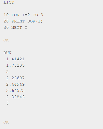
A small test program:
![]()
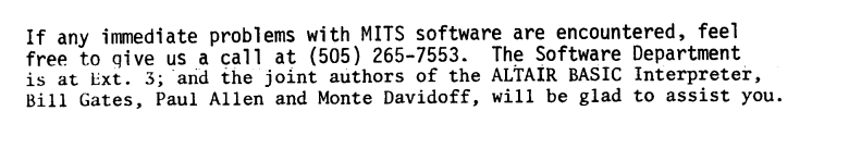
Yes, it does floating point ! If want to know what it can do look in the Altair BASIC reference manual. And if you program in this basic and encounter a problem, some help is never far away:
![]()
-
Javascript emulator runs Apple 1 BASIC
05/09/2023 at 18:43 • 0 commentsThe emulator is ready (in Javascript), and the microcode that makes Isetta a 6502 was also completed. The emulator mimics the operation of the hardware, so it needs the same microcode.
What could be better to test it, than the original BASIC of the Apple 1 ?
There were a few mistakes in the microcode, the BIT instruction did not set all flags correctly, and the LDX/LDY-immediate did not set the flags. And originally I thought I could do without the overflow flag, but the Apple BASIC uses it, so I changed my mind and also implemented this.
Here is the proof that it is working:
![]()
After the basic is loaded in the memory of the emulator, a few patches are done to enable keyboard-input and textarea-output. It is amazing that you must jump through several hoops to convert javascript-keystrokes in 'normal' ASCII.
-
First 6502 microcode
04/22/2023 at 10:16 • 0 commentsA first version of the microcode was made. The microcode is generated with a Javascript program. The script can be downloaded from the file section. An effort was made to make the microcode as clear as possible, the output will be a list of microcode instructions with a good explanation, for all 151 opcodes of the original 6502. It lookes like this:
---- 0xC8 INY reg_y ----
001900 3A84B3 3A84B3 to_t <- inc(reg_y),upd_nz
001902 008301 008301 next
001904 11B403 11B403 reg_y <- acc_t

---- 0x69 ADC imm ----
000D20 D1AB80 D1AB80 to_dpl <- (pc++),irq_to_f
000D22 5D46F0 008301 F:[to_a <- adc(acc_a, dpl),upd_nzc] T:[next]
000D24 000401 5D46F0 F:[interrupt] T:[to_a <- adc(acc_a, dpl),upd_nzc]
000D26 110400 110400 int2

---- 0x65 ADC zp ----
000CA0 D1AB80 D1AB80 to_dpl <- (pc++),irq_to_f
000CA2 5DC5F0 008301 F:[to_a <- adc(acc_a, (0|dpl)),upd_nzc] T:[next]
000CA4 000401 5DC5F0 F:[interrupt] T:[to_a <- adc(acc_a, (0|dpl)),upd_nzc]
000CA6 110400 110400 int2

---- 0x75 ADC zpx ----
000EA0 D18B80 D18B80 to_t <- (pc++),irq_to_f
000EA2 1DA402 1DA402 to_dpl <- add(acc_t, reg_x)
---- end of ea calculation ---
000EA4 5DC5F0 008301 F:[to_a <- adc(acc_a, (0|dpl)),upd_nzc] T:[next]
000EA6 000401 5DC5F0 F:[interrupt] T:[to_a <- adc(acc_a, (0|dpl)),upd_nzc]
000EA8 110400 110400 int2
You can easily generate the full microcode:
- Go to: this W3Schools page.
- Clear the text in the left window and paste the microcode-generator code there.
- Press Run
- The microcode will appear within a few seconds.
Some remarks about the notation:
- The first hex number on a line is the address in the microcode ROM
- The next two hex numbers are the microcode. These numbers are the same, except when conditional execution is used
- When there is no interrupt, only the T:[ ... ] sections are executed.
- When there is an interrupt, the F:[ ... ] sections are executed.
- 'next' is an indication that the next opcode will be loaded. Due to the pipeline effect, one extra instruction will be executed after 'next'.
- Depending on its role in the instruction, register A will be shown as 'to_a' or 'acc_a'. Same for register T.
It is easy to count the number of cycles for each opcode. Just count the lines up to the first instruction that contains 'next', then add one cycle for the instruction after 'next'. So the shown 'ADC zp' opcode takes 3 cycles.
The operation of some instructions will probably still be unclear to you. In that case, check the microcode script that contains a lot of comments about the used instructions.
In the microcode generator, there is a central role for the function 'ins6( a, b, c, d, e, f )'. The name 'ins6' stands for 'instruction with 6 components'. The six components are:
- a. Condition. An instruction to move a condition to the F flag, like c_to_f, z_to_f, or irq_to_f.
- b. Destination. Data destination, like to_t, to_a, to_dpl.
- c. ALU operation, like ld, adc, and, rol.
- d. Source 1, this can only be acc_a or acc_t. For single-operand instructions, source 1 is unused. For writing to memory it decides if A or T gets written.
- e. Source 2, this will in most cases be a memory location, like 'dir' (zpage location), 'ext' (full 64k range address in dph|dpl), 'pc_pp' ( (pc++) ), or a hardware register (dph, dpl, pch, pcl), or a register location in memory (like reg_s, reg_x), or a small constant lit0, lit2, lit8, lit32 for the values 0, 2, 8, 32. For writing to memory, source 2 is the destination address.
- f. Update flags. It is indicated as upd_nz, upd_c, upd_nzc. Any combination of N, Z, C flags is allowed.
The ins6 simply combines the control-wire values of its arguments, so it would not matter in which order the components are placed. But the comment-printing function 'pr_print' depends on the order of this components.
It is tempting to continue with writing the Z80 micro-instructions, but I will now first make a simulator to check if everything works as intended.
-
Control section details
04/15/2023 at 21:15 • 0 commentsIn this log I talk about the 24 control signals that come from the microcode. The names of all signals that come from the microcode register will start with CTL.
[ EDIT March 2024. Since the writing of this log, several details have changed, so this log is no longer fully accurate ]
The microcode will be organized in 3 bytes, the upper, middle, and lower control byte. The upper microcode has the longest description.
MICROCODE UPPER CONTROL BYTE
The first diagram shows the signals that select a condition and handles flags:
![]()
Flag update
Some instructions update flags, others don't. The signals CTL_UPD_C, CTL_UPD_Z and CTL_UPD_N indicate if the flags C, Z or N must be updated with a new value coming from the ALU_COUT, the ZERO detector at the output of the ALU, or bit 7 of the ALU output (R7, Result-bus bit7). If a flag is not updated, it will keep the same value.
There is no provision to read or write the flag bits as a full byte, like that is normally used in many 6502 designs. The microcode will have to read or write the flags one-by-one in order to push or pull the flags (or do EX AF,AF' for Z80).
Condition select
The signals CTL_C0, CTL_C1 and CTL_C2 select one of eight conditions. It is used for two different things:
- As a selector of the CONDITION carry-in signal of the ALU (adder or shift-right)
- As a selector for the FLAG_F for conditional execution. This second function is activated when CTL_WR_F is active (high). If CTL_WR_F is low, FLAG_F keeps the same value.
Early condition evaluation
There is one more important thing to say about the condition selection. Suppose that we want tot test for a condition, and execute a conditional micro-instruction based on that, this would be 3 micro-instructions (3 cycles):
- Select the relevant condition, like C, Z or N, (putting this condition in FLAG_F)
- Fetch the next micro-instruction based on the FLAG_F value
- Execute the micro-instruction that was selected with FLAG_F
Number 1 and 3 are really needed, but in number 2 we are just waiting for the next micro-instruction coming out of the pipeline, and if we can not do something useful in that cycle, it is a 'lost cycle'. But we can do something about that. By connecting the signals CTL_C0, CTL_C1, CTL_C2 and CTL_WR_F not to the microcode register, but directly to the microcode ROM output, we can evaluate the condition one cycle earlier (at the end of the fetch phase). We now get the following two-cycle sequence:
- Select the condition. The selection has actually been done in the previous cycle, so in this cycle the new micro-instruction, based on the FLAG_F value, will be fetched.
- Execute the micro-instruction that was selected with FLAG_F
So we just gained one cycle for micro-instructions that use conditional execution.
ALU CONTROL
![]()
The ALU control section must provide the control signals for the ALU. In the ALU log it is shown that the following control signals are needed:
- 4 bits DCBA controls for the upper logic unit
- 4 bits DCBA controls for the lower logic unit
- 2 bits Carry-input signals for added (ADD_CIN) and right-shift (SHR_CIN)
- 1 bit selection of shift-right unit CTL_SHR
So the ALU can be controlled with 11 signals. But we don't want to spend so many of the available micro-instruction bits for these. Fortunately, it is not difficult to bring this number of signals down to a reasonable amount.
Generating the DCBA control signals
The DCBA controls for the upper logic unit have bit A being '1' only in the case of a DEC instruction (and for complementing a value, but we don't use that). So bit A can be removed from the control wires and be regarded as a special case.
The DCBA controls for the lower logic unit only use the patterns 0000, 1010 and 0101. Of these, the 0101 is only used in a single case (SUB, Subtract), so if we handle that as a special case we only need a single control signal CTL_ALU0 for choosing between 0000 and 1010.
To handle the special cases, we have a decoder (U5) that decodes the CTL_ALU1, CTL_ALU2 and CTL_ALU3 lines into 8 separate cases. The output of the decoder is activated (high) when the ALT/ signal is low. It handles the DEC and SUB cases and will also control the right-shift (CTL_SHR) as a special case.
Group 0 and group 1
The ALU operations are divided in two groups, selected by CTL_ALU3:
- Group0, when CTL_ALU3 = 0
- Group1, when CTL_ALU3 = 1
Group1 is the easiest to understand, this encompasses all arithmetic instructions (although also some logical instructions are in this group). The multiplexers at the right side of the drawing will do the following:
- U1 will connect the CONDITION to the carry-input of the adder
- U2 will connect the carry-output of the adder to the ALU carry result
- U3 will update TC (temporary carry) with the value of the carry-output of the adder
- U4 will connect CTL_ALU2 to bit C of the upper logic unit, providing all 1xx0 functions
Group0 encompasses instructions where the adder is only used as pass-through, for some logic functions, for shift-right and for loading (moving) a value. This is also the group to use for writing a new value to FLAG_F. A single micro-instruction can write to FLAG_F and load a new value (at the same time). Multiplexer functions for group0 are:
- U1 will disconnect the carry-input of the adder from the CONDITION. If the condition is used to write FLAG_F or to provide carry-input to shift-right, the adder should pass-through any value unchanged, and having a signal on its carry-input would spoil the pass-through.
- U2 will connect databus bit D0 to the ALU carry result, for the case that a shift-right is done, where D0 is shifted out of the byte and can be put in the carry C.
- U3 will load TC with its own value, so it will not change. So when a byte was added to a low byte and this might have set TC, we can do some data move instructions afterwards, and still have the TC available to use it when adding something to the high byte.
- U4 will connect bit C of the upper logic unit to output 001 of the ALT decoder (U5). This makes the value 0000 appear twice in the range of codes. This is a useful code because it enables the LD (pass) function of the ALU. Having two LD functions means that we can combine it with two different special ALT cases (to be discussed later). When the output 001 of the U5 decoder is selected, we can use the ALT/ signal to switch between 0010 (RES function) and 0110 (EOR/XOR function). The RES function is a bitwise logical function, that resets a bit coming from the databus when a bit on the operand bus is set (useful for Z80).
Summary of upper control byte
The upper control byte has the five ALU controls in bits0-4 and the three condition selects in bits 5-7. The following diagram shows the ALU micro-instructions that are possible with the upper byte:
![]()
- The functions that need an active ALT are shown in red, and the control bits in the upper and lower logic units are also in red if they are modified by this ALT function.
- You can see in column 1 that the LD function can be combined with every condition (to be put in FLAG_F)
- In column A there is also a (LD) function but this does not have the benefits of the LD in group 0.
- All empty positions will also perform functions but these functions will in many cases not be useful.
MICROCODE MIDDLE CONTROL BYTE
This will provide the following control bits (explained below):
- bit7 CTL_SRC
- bit6 CTL_DST2
- bit5 CTL_DST1
- bit4 CTL_DST0
- bit3 CTL_WR_F (see condition select at the beginning of this log)
- bit2 CTL_REG3 (extension to reg0/reg1/reg2 in lower control byte)
- bit1 CTL_M1
- bit0 CTL_M0
Source and Destination
Most bits in this byte determine how the information flows in the CPU. A source and a destination are selected. The CTL_DST0, CTL_DST1 and CTL_DST2 determine the destination of a byte on the result bus:
- 0, Register T
- 1, DPH register
- 2, DPL register
- 3, Memory
- 4, Register A
- 5, PCH register (PCL will at the same time be loaded from DPH)
- 6, VRAM (Writes to video RAM)
- 7, Output (to be defined later)
The bit CTL_SRC determines the source for the databus. For destinations Memory and Output, the source is:
- CTL_SRC = 0, source is the lower control byte of the microcode register
- CTL_SRC = 1, source is the operand bus (with destination Memory, used for storing register A or T to memory)
For destinations other than Memory or Output, the source is:
- CTL_SRC = 0, source is a byte coming from the high or low address bus (see CTL_HI in lower control byte)
- CTL_SRC = 1, source is a byte coming from memory
Address
Almost all source and destination combinations need an address on the address bus. The address is determined by the CTL_M0 and CTL_M1 signals:
- 0, a register stored in memory, addressed by the CGL constant as low byte and a zero as high byte
- 1, a zero page address (for 6502), addressed by the DPL register, with high byte zero
- 2, the program address, addressed by PCH and PCL
- 3, a full 64k address, provided by DPH and DPL
When the program counter is used to address memory, it will also increment. But if it's only used to access its value (like for storing a return address), it is not incremented.
MICROCODE LOWER CONTROL BYTE
This will provide the following control bits (explained below):
- bit7 CTL_ACC_A (If high, A is on operand bus. If low, T is on operand bus)
- bit6 CTL_UPD_C (tells if C flag must be updated)
- bit5 CTL_UPD_Z (tells if Z flag must be updated)
- bit4 CTL_UPD_N (tells if N flag must be updated)
- bit3 CTL_HI
- bit2 CTL_REG2
- bit1 CTL_REG1
- bit0 CTL_REG0
When the source is coming from the high or low address bus, it comes from the high address bus if CTL_HI is '1', and from the low address bus if CTL_HI is '0'.
In the register addressing mode, the lower 3 bits specify 8 registers. If the CTL_HI bit is set, it specifies 8 other registers, but in this case there is an extra address bit that is provided by the Z80-exx flipflop. The result is that the upper 8 registers can be swapped for other registers by toggling this flipflop. It implements the alternative register set of the Z80.
Well, that's it. I hope I didn't forget a control bit.
The drawings in this log were made with Scheme-it.
-
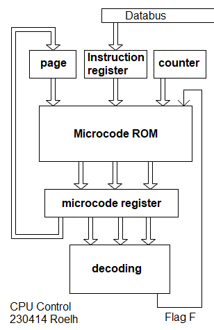
CPU control section
04/14/2023 at 20:45 • 0 commentsThe following diagram shows the principle of the control section:
![]()
START OF NEW INSTRUCTION
As said before, the processor is controlled by microcode. At the start of a new 6502 or Z80 instruction, the opcode of that instruction will be put in the 8-bit instruction register and the counter will be reset to zero. The counter has 4 bits, so for each opcode in the instruction register there can be a sequence of maximal 16 micro-instructions.
SEQUENCE
The Microcode ROM will deliver the 24-bit micro-instruction and store it in the microcode register at the end of the cycle. At the end of the cycle, the counter is incremented to prepare for fetching the next micro-instruction. In the next cycle, the micro-instruction is decoded (in the decoding block) and the micro-instruction is executed.
For each opcode, there is a unique sequence of micro-instructions that will be executed. At the end of this sequence there is a special micro-instruction called LD_IR that loads the new opcode in the instruction register, resets the counter, and sets the 4-bit page.
PIPELINE
Note that when the micro-instruction is executed, the following micro-instruction is already being looked up in the microcode ROM. This means, that when the decoding section decides that a new opcode must be put in the instruction register, the next micro-instruction is already read from the microcode ROM. So the LD_IR is not the last instruction in the sequence: The micro-instruction that follows LD_IR will also be executed. This is the pipeline effect.
CONDITIONAL EXECUTION
The control unit is capable of conditional execution of micro-instructions. At each location in the microcode ROM, there are actually two instructions stored. Which of these is fetched, is determined by a flag called F. If, for a certain instruction, we do not want it to be conditional, we simply store two identical instructions, so in that case it doesn't matter which one is executed.
PAGES
If we would only have 6502 instructions, the page register would not be needed because there are only 256 possible opcodes (of which many are unused). But a Z80 would need several pages, because in its basic set of 256 opcodes there are some that are followed by another opcode byte. It is expected that the Z80 can be handled in 5 pages (A basic page, index IX and index IY page, shift-and-bit page, and the 0xED page for the special Z80 instructions). So of the 16 available pages, 1 will be needed for the 6502 and 5 for the Z80. The page register can be changed by the LD_IR instruction.
-
Requirements for the control section
04/06/2023 at 20:21 • 0 commentsMicro-instructions... which instructions do we need ? Before the control section can be designed, we need a list of everything that we want to control with a microinstruction.
[ EDIT March 2024. Since the writing of this log, several details have changed, so this log is no longer fully accurate ]
We start with a short list of pseudo-code that will have to be supported, it tells how the information will flow and what the ALU does:
// Load Instruction Register with next opcode. It would be nice
// if it can also be loaded from another source. This micro-instruction must
// also specify which microcode page to use for the next opcode. Each microcode
// page has room for 256 opcodes of max. 16 microinstructions each.

    IR <- (PC++)

// Instructions with a single operand.
// op1 can be LOAD, INC, DEC, SHR

    dst_reg <- op1 (data_source)

// Instructions with two operands. Can use A or T register as first operand.
// op2 can be ADD, SUB, ADC, SBC, AND, OR, XOR

    dst_reg <- op2 (A, data_source)
    dst_reg <- op2 (T, data_source)

// Store instructions. Only A or T can be stored.

    mem(address) <- A
    mem(address) <- T
The dst_reg can be A, T, DPH, DPL, PCH. When PCH is written, DPH will be written to PCL
The data_source can be:
- a register (DPH, DPL, PCH, PCL),
- a small constant (CGL)
- a value read from a memory address.
A memory address can be:
- a register stored in memory, addressed by the CGL constant as low byte and a zero as high byte
- a zero page address (for 6502), addressed by the DPL register, with high byte zero
- a full 64k address, provided by DPH and DPL
- the program address, addressed by PCH and PCL. Automatic increment of PCH/PCL after it is used.
The register that is stored in memory sits in a special 64K memory area called SYS. It is addressed by the CGL constant (4 bits). The lower 3 bits specify 8 registers. If the 4th bit is set, it specifies 8 other registers, but in this case there is an extra address bit that is provided by the Z80-exx flipflop. The result is that the upper 8 registers can be swapped for other registers by toggling this flipflop. It implements the alternative register set of the Z80.
ALU FUNCTION
The control section has to tell the ALU what it should do:
Two-operand instructions like ADD, SUB, AND, OR, EOR
One-operand instructions like LD, INC, DEC, ASL, LSR, ROL, ROR
FLAGS
But the microinstruction has to specify more:
- which processor flags ( N, Z, C ) to update
- if the internal carry flag (TC, Temporary Carry) must be updated (see below)
- which value to use for the carry-input of the ALU and for the SHR block ( 0, 1, C, TC )
- which condition to use for conditional execution (see below)
The Temporary Carry is a flag that is used for address calculations, in situations where the programmer-visible C flag must not be changed.
CONDITIONAL EXECUTION
The control unit is capable of conditional execution of microinstructions. At each location in the ROM that stores the microinstruction, there are actually two instructions stored. Which of these is fetched, is determined by a flag called F. If, for a certain instruction, we do not want it to be conditional, we simply store two identical instructions, so it doesn't matter which one is executed.
This flag F can be modified by the microcode. For example, in a BCS (branch on carry set) instruction, the flag F will first get the same value as the C flag. The following microinstructions will now put the jump-address in the program counter when the F flag is '1'.
Another use is, that the Interrupt-signal can be copied to the F flag at the beginning of the microcode for an instruction. At the end of the microcode sequence, the F flag will then be tested, and if there was an interrupt, the instruction register (IR) will be loaded with the opcode of the instruction that handles the interrupt. (That will probably be an opcode in an other page.)
The F flag can be set to one of the following conditions:- N flag
- Z flag
- C flag
- TC flag
- databit D0
- databit D7
- Interrupt
- (unused)
Using databit D0 or D7 provides a way to do carry handling for shift instructions. D7 is also copied to F to do sign-extension of the offset for a branch (relative jump).
SPECIAL INSTRUCTIONS
Some special instructions will be required for writing to the video memory, providing fast block-copy instructions, and input/output instructions.
The Z80 has instructions that test, set or reset a bit in a register or memory location. So it will be good if there are some microinstructions to support this. This will be providing a bitmask from a CGL value, and providing RES instructions that reset a bit in the destination byte when the corresponding bit in the bitmask is set.
The provided set of 8 registers and 8 switchable registers might not be enough for some situations. So an extra address bit will be provided that doubles the amount of available registers, but this extra bit can not be used in combination with every microinstruction.
CONCLUSION
After fiddling around with all the requirements, I found that the number of bits in the microinstruction must be 24.
-
The ALU of Isetta
04/01/2023 at 14:35 • 1 commentWhich functions do we need in the ALU and how must that be arranged? Well, we need the usual ones:
Arithmetic:
- ADD (Add two bytes)
- SUB (Subtract one byte from the other)
- INC (Increment: Add 1 to a byte)
- DEC (Decrement: Subtract 1 from a byte)
Logic:
- bitwise AND
- bitwise OR
- bitwise XOR (called EOR for the 6502)
Shifts:
- Shift the bits in the byte one bit to the left (For ROL and ASL on the 6502)
- Shift the bits in the byte one bit to the right (For ROR and LSR on the 6502)
Pass:
- PASS Pass data from databus unmodified.
It must be possible to pass a byte from the databus to the output of the ALU, because otherwise it would not be possible to simply load a value in one of the registers (it is needed for LOAD functions).
The ADDER
The ADD function is easy to realize. There is a chip that can add two 4-bit values, it is called the 74AC283. If we use two of them, we can add two bytes that are present on the A and B input of the adder. The chip has a 'carry' input that can be connected to the Carry flag to provide ADC (Add with carry).
We need a way to connect the A-input of the adder to zero, this causes the B-input (databus) to be added to zero, passing the databus value to the output, providing the PASS function. If we set the carry-input of the adder to logic 1, this function will become INC.
If we connect the A-input of the adder to the value 0xFF (all 8 bits '1'), the adder will add the value 255 to the B-input (databus). But this is a value greater than 8 bits ! The 8th bit will be dropped and the result is that the databus value is decremented, so we now have DEC.
And we need a subtract function, SUB. This can be calculated by bitwise complementing (replacing 0 by 1, and 1 by 0) the B-input, and then ADD (while providing '1' on the carry input). The 'carry' input can be connected to the Carry flag to provide SBC (Subtract with carry).
Left shift can be done by adding a value to itself. The microcode will handle that, so the 6502 or Z80 functions to shift left will work as usual. The right shift needs a dedicated chip.
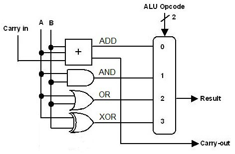
A simple way to do LOGIC functions
For providing logic functions, the easiest way to do that seems to be to build something like the following circuit:
![]()
This not only provides the logic functions, but also ADD. It is very easy to understand, the left side of the diagram calculates the ADD, AND, OR and XOR functions, and at the right side the ALU Opcode selects which of the four results will be used (with a 4-input multiplexer). It will work perfectly.
How many parts will be needed ?
Since this is an 8-bit ALU, we need 8 gates of each type. There are 4 gates in a chip, so calculating the three logic functions cost 6 chips. We need eight 1-bit multiplexers, there are two in a chip, so that cost 4 chips, and there are the two adder chips, for a total of 12 for the circuit above.
But there are more chips needed. For subtract, the B input must be complemented, that can be done with two 74HC86 XOR gate chips. And for INC or DEC we must be able to put a value of 0 or 0xFF on the A input. This can be done with two multiplexers 74HC157, that can connect the A-input either to the input bus or to the fixed value 0 or 0xFF. That is 4 chips for these special functions, bringing the total to 16 chips for the ALU.
Calculating Logic functions with less chips
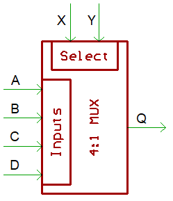
In the previous section we used a multiplexer. It has two inputs X and Y that select one of the inputs A, B, C or D and put the selected signal on its output Q:
![]()
The truth table of this device is:
X   Y   Q
----------
0   0   A
0   1   B
1   0   C
1   1   D
If we now regard X and Y as inputs and A, B, C and D as constants, we actually have a programmable logic gate, where the value on the four ABCD inputs determines which 1-bit function it performs on the values X and Y:
DCBA
0000  Always 0
1000  AND
1110  OR
0110  XOR
1100  pass value X
1010  pass value Y
0011  pass value X complemented
0101  pass value Y complemented
1111  Always 0xFF
This is also explained in this page of Dieter Mueller. So this simple device can do all required logic functions and provides a simple way to select which function it should perform. The same trick was used in the 8086 processor, described in this article by Ken Shirriff about the ALU of the 8086.
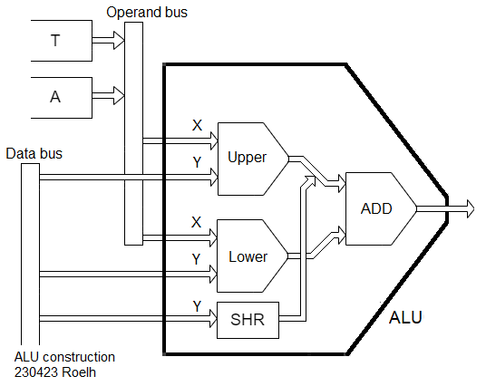
There are two of these devices in a 74HC153 or 74AC153 chip. So for 8 bits we need 4 chips ? That would be very nice, but unfortunately, it is not true. Both two internal multiplexers of this chip have the X wires and Y wires connected to each other, as common inputs. So we need 8 of those chips. But what to do with the now unused second device in each chip ? Well, we can build TWO logic units, that share the same inputs X and Y, and that each have their own Q outputs. We then connect both Q outputs to the input of the adder:
![]()
The two logic units are called Upper and Lower. The Upper and Lower logic unit each have their own ABCD control value. Now it is easy to have the extra functions that we need, a complement-circuit for subtraction (in lower logic unit), and a fixed value 0 or 0xFF (in upper logic unit).
The only function that is missing is the shift-right (For ROR and LSR on the 6502), so a SHR circuit that shifts the bits to the right can be used instead of the upper logic unit. For shifting right, the output of the lower logic unit must be zero. [edit 231025 : I later decided that there will not be a SHR unit, to save parts. SHR will be done in microcode, with a table in memory]
The adder will add the results of both logic units. This gives the following functions:
Upper      Lower
Logic      Logic
DCBA       DCBA
--------   --------
1100 (X)   1010 (Y)     ADD Y to X
1100 (X)   0101 (not Y) SUB Y from X (need Cin = 1)

0000 (0)   1010 (Y)     PASS Y (with CY: INC Y)
0000 (0)   0101 (not Y) CPL Y (bitwise complement Y)
1111 (FF)  1010 (Y)     DEC Y

1000       0000         AND
1110       0000         OR
0110       0000         XOR
Note that for all functions, we can swap the ABCD values of both logic units without changing the final result.
The function of the ALU is now controlled by the two 4-bit ABCD values. These two 4-bit values will be provided by the control section of the CPU.
In the control section of the CPU, there will be another multiplexer circuit that uses two control bits to select one of the following four sources for the carry-input of the adder:
- 0
- 1 (Needed for SUB and INC)
- C (Carry flag, needed for ADC and SBC)
- TC (Internal Temporary carry flag, used for address calculations)
This ALU is only 11 TTL chips (10 without the SHR unit), instead of the 16 for the simple design in the previous section.
We are in good company, the same ALU principle is used in the C74 6502 TTL design and in the Gigatron.
Isetta TTL computer
Retro computer built from TTL, with 6502 and Z80 instruction set. Includes video, sound and filesystem. No microprocessor or FPGA.