-
Project Finished !
02/18/2026 at 14:58 • 0 commentsNew software pack
In the file section, you find a new software pack sw_pack260212.zip. I has the beta version of SymbOS version 4.1 for the Isetta, and a new microcode version.
This software fully supports:
- the 1024kB Isetta, but also the 512kB version
- several languages (English, Dutch, German, Spanish, Turkish and Japanese)
- several character pages, the main one is based on CP-1252It supports PS/2 keyboard layouts for Brazil, France, Germany, Greece, Hungary, Italy, Japan, Netherlands, Poland, Portugal, Spain, Turkey, Ukraine, United Kingdom and USA.
The Isetta project can now be regarded as finished, although I expect that there will be a few software enhancements.
Isetta at MSX fair Nijmegen
On march 28th you can come to Beuningen-NL (near Nijmegen) to see Isetta ! Isetta will be at the SymbOS booth at the MSX fair (free entrance).
Jörn Mika (creator of SymbOS) and I will also be there.
See this link: https://manuel.msxnet.org/msx/beurs/?lang=enIsetta built by Walter Belgers
And here you see a very nice Isetta built by Walter Belgers from the Netherlands.
![]()
![]()
Perhaps not clearly mentioned before, Isetta can directly drive a speaker (but you can also use the 3.5 mm sound output).![]()
-
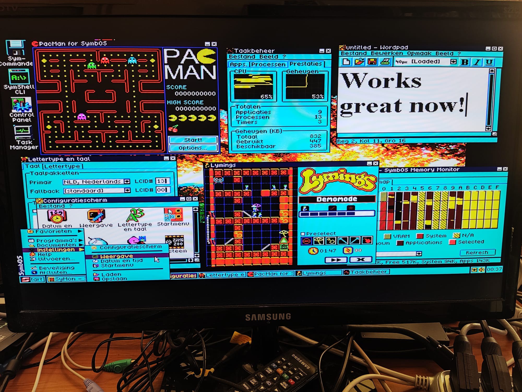
SymbOS has the full one Megabyte !
01/27/2026 at 08:34 • 0 commentsSince a few days, the SymbOS operating system can use the full megabyte of memory on Isetta. The adaption was done by Prodatron, the genius that designed and programmed SymbOS.
![]()
Here is a screenshot of the 1 MB system. At the lower right side you see the memory map, the numbers 0 - F are the sixteen 64K memory banks. The yellow banks from B - F are still available !
One megabyte is the maximum amount of memory that SymbOS can handle. This means that the Isetta version is now just as capable as the SymbOS versions for all other platforms.
If you take a close look, you will see that many of the menu items and texts are now in Dutch ! Symbos will soon have a new feature, the support for several languages other than English. It will then also work with PS/2 keyboards for those languages. The first supported languages are Dutch, German, Spanish, Turkish and Japanese (really). French, Italian and Greek will be the next ones.
-
A Detective Story
12/27/2025 at 15:40 • 0 comments"Just another day at the Sam Cruise Detective Agency. I hear the staccato rattle of Daisy at the old typewriter in the outer office: the band in my head starts to tune up. I reach for a strong coffee. Pulling up the blind I look out of the grimy window into the street below. Ordinary people going about their ordinary business, unaware of the intrigues on their doorsteps. What do they know of the Fat Man, or the mysterious goings on at No.19?. Luscious Lana wiggles past, a sly smile playing across her ruby red lips. A gust of wind disturbs the garbage on the sidewalk.
And then the phone rings... "
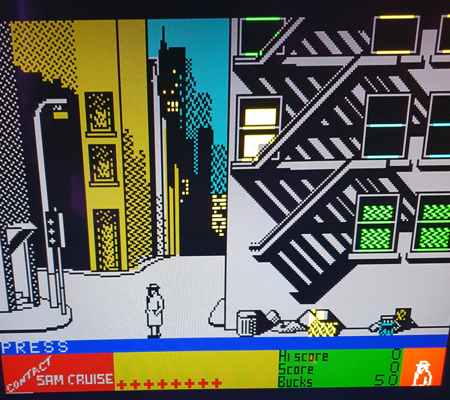
Since a few days, a new (old) game is running on Isetta: Contact Sam Cruise (CSC)
![]()
It's a ZX Spectrum game from 1986. You are the detective who has to solve a murder case. Very nice graphics.
![]()
Running ZX Spectrum games
Since a few months, Isetta boots the SymbOS operating system directly. That implied that there was no fast way to run Spectrum games from internal serial flash, as before, when also SymbOS had to be started from this flash chip.
But I now have a new way to start Spectrum games from the SD card. And I added the Sam Cruise game.While Manic Miner and The Great Escape directly approached the hardware through I/O ports, the Sam Cruise game relies on interrupt handling by the spectrum ROM. When a frame interrupt occurs, the ROM software increments a frame counter at 5C78 (that is used by CSC to start drawing a new frame), and it reads the keyboard matrix, converts to ascii and put that on location 5C08, where CSC reads it to decide which command you entered.
The games can be entered in assembly , and can then be assembled with WinApe (Amstrad simulator and assembler) on a PC, resulting in a ".com" file. I made a special include file "zx_incl.asm" for this, that is a software layer that lets Isetta behave as a ZX Spectrum.
It switches the screen to ZX Spectrum mode, converts ps/2 keyboard signals to ascii, and handles an interrupt as described above. For games that read the keyboard matrix directly through an INPUT port, it simulates the ZX keyboard matrix.
Note that on Isetta, IN and OUT instructions do not simply transfer bytes on the databus. They call a sequence of microinstructions that can do almost anything.In general, ZX programs run without modification. But Manic Miner ran a lot too fast, due to the fast LDIR that Isetta has. I created a second LDIR (opcode ED B4) that has the same speed as on a real Z80 and used that. Now, Manic Miner has normal speed. And in a few games I disabled the automatic joystick detection.
More spectrum games (in assembly) can be found here: https://gitlab.com/z80-source-code-software/other-systems/
How to run a Spectrum game
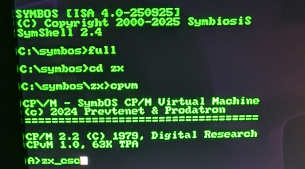
On the Isetta computer, start the SymShell by double clicking on it's icon.
If you like, select a full screen with the "full" command.![]()
Change the directory (with CD command) to the ZX directory where the .com file and cpvm.com are.
Then type "cpvm" to start the CP/M operating system,
and in CP/M, type the name of the .com file (you can omit the .com part), to start it.
![]()
The following games are available:
zx_mm.com // Manic Miner
zx_tge.com // The Great Escape
zx_csc.com // Contact Sam CruiseAlso, the full assembly code of these games is provided. It includes the software adaption layer that lets Isetta behave as a ZX spectrum (Video, keyboard and sound). This will also enable you to run other ZX Spectrum programs.
New software pack in file section
Today I uploaded a new software pack to the file section of this project, sw_pack251227.zip.
It has several new things:Symisa.pak // An improved SymbOS version that starts programs faster
Symbos.ini // Was missing in previous pack, causing programs that refused to start
isetta_rpi // Improved automatic test
zx // New directory with ZX Spectrum games
ucode251203 // New microcode needed for new ZX games and improved SymbOSIt is not needed to re-write all microcode. Just compare each page with the Verify command, and only re-program that page if there was a difference.
[edit: It seems Manic Miner works on the 1024k version but not on the 512k version. Have to investigate this. ]
-
One Megabyte !
11/29/2025 at 21:20 • 0 commentsThe SymbOS operating system runs fine on Isetta. But when you have several programs open, and use a few of it's advanced options, the 384kByte available memory on a 512kB system is in many cases not enough.
Therefore, I added another 512 kByte RAM to Isetta. The bankswitching system got an extra chip to handle the extra address bit, and a quick pcb redesign was done. The pcb was built, and a low-level memory test proved that the extra RAM was working.
Work to let SymbOS use the extra RAM is still in progress, and hopefully can be finished soon.
If you order a kit, you will get the 1024 kByte version from now on.
-
More documentation online
10/05/2025 at 07:57 • 0 comments
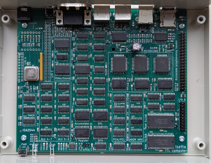
In the Hackaday file section, I now placed the almost-latest version of the schematic, and 3 assembly drawings that will make it easy to find the components on the pcb when you build it. For convenience, the typenumbers of the IC's are printed on the pcb.
The new pcb's (ISA2532) have arrived from my sponsor PcbWay. As always, the quality is very good and they deliver quite fast.
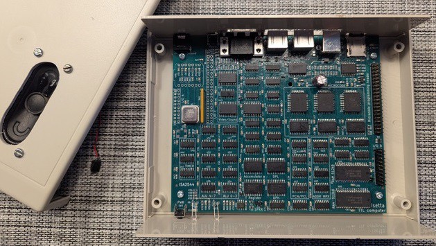
Builders of the KIT will now receive this pcb, so there is no need any more for the modifications with all the wires. The pcb was tested by building an Isetta with it, and it works perfectly.The SymbOS version for Isetta is now practically bug-free.
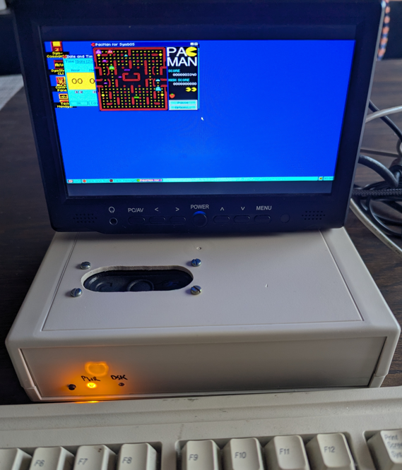
SymbOS has a shutdown command, that switches VGA screen and the power LED off. After pressing the button at the front, it will start-up again.
The real-time clock/calendar is now also working. It keeps running during shutdown, and during ZX-Spectrum or other applications.
On october 11th/12th, Isetta will be at the SymbOS stand in the Nixdorf Museum in Paderborn (Germany):
https://www.hnf.de/veranstaltungen/events/date/2025/10/11/cal/event/tx_cal_phpicalendar/retro-computer-festival-1.htmlFor all of you who want to build one, I sell pcb's on my new Envionic website (not a HTTPS connection possible yet).
-
Third PCB design finished
07/30/2025 at 08:40 • 0 commentsThe new pcb design was finished. I did not send it yet for production, because experience says, that within ten minutes of the final submit for production, I think of something that I forgot in the design. So I just wait a few days before ordering.
What changed (w.r.t. ISA2442 version):- The wire modifications, as on prev version, are no longer needed
- slightly changed form factor, to better fit in the housing
- Have a 1.5 W sound amplifier on board, can now directly connect a speaker. The
output for an amplifier is also still on board.
- Due to speaker dimensions, a bigger housing is used, RM2055M (instead of RM2055S)
- Have a 'wakeup' button at the front. (A SymbOs command can put Isetta asleep). The power
LED will be off while Isetta is asleep.
- Several changes to improve EMC behaviour
- Amount of Microcode flash ROM can be doubled, now 32 instead of 16 microcode pages.
(The option to use 8-cycle instructions was removed for this.)
- Max number of consecutive microcode cycles is now 512 (was 256). Now it is easier
to display 640 pixels per line (two pixels per cycle, so 320 consecutive cycles)
- The selection between 640 or 320 pixels per line is simpler now (uses ctl_upd_n)
- The 4 blinkenlights were removed
- Added a LED to indicate file read/write
- Changed the optional WiFi module to XIAO ESP32S3 (WiFi + Bluetooth BLE)
- The WiFi module has an option to add LoRaWan
- One extra IC used. And one for the sound amplifier.New Option connectors:
- I/O A: 20 pin connector. Bus for parallel input/output. Has 8 datalines, 3 address lines.
- I/O B: 20 pin connector. Supports 4 input and 4 output bits. Also useable for alternative power
supply (and battery backup). This option can also select a lower CPU speed
for less power consumption.
- I/O C: 40 pin connector. A board to give more video modes can be connected here.- I/O D: 20 pin connector. Connects to RPi. This was "I/O C" on prev version. Removed some unused signals.
This is the 3D impression of KiCad:
![]()
-
We have Sound !!
06/10/2025 at 09:24 • 2 commentsFinally, the PSG (Programmable Sound Generator AY-3-8910) is coming to life. It was harder than I thought. But it now has the 3 channels for tone or noise, with independent frequency and volume control. Only the the envelope generator is not present yet [edit: a month later, envelope was also working]. The sound is generated by microcode, no actual AY-3-8910 is used, but the sound is controlled in the same way as on a real sound chip.
It generates the typical sound of the eighties computer games.
It can now provide sound for the SymbOs operating system ! And here you see the first Youtube video of Isetta running SymbOs (made by Prodatron):
(The start-up screen of Isetta will have to be modified, it's quite a mess at the moment.)
A new version of the Isetta programming manual is now in the file section. It includes the commands to control the sound generator.
OPERATION
There are four 1 kB sound buffers, one for each of the three channels, and a fourth one for noise.
The squarewave sounds are generated in an unrolled loop. So if a wave has 5 samples 'high' and 5 samples 'low', to generate one period there will be two sequences that each put samples in the buffer, with each having five "(pc++) <- T" micro-instructions in a row. (Note the program counter is used as auto-incrementing pointer to the buffer).
The value in T is the required amplitude for this sound (positive value for high samples, negative value for low samples). So there is no separate volume-control stage, like the real PSG has.
At each scanline interrupt, a byte-sized sample is taken from each of the four buffers, the four samples are added and sent to the D/A converter (resistor array RN1). So the sample frequency is the same as the VGA line frequency, 31.25 kHz.
To control this, there are two Z80-output ports. One to select a AY-3-8910 register, and another one to write a byte to that register. The Z80 output ports can also be used by the 6502 processor.
EFFICIENCY
For each channel, producing samples takes around 3 cycles per sample. (The unrolled loop produces 8 samples on average, single cycle per sample, with also 16 cycles overhead).
For a full 525-line frame, this is 1575 cycles per channel. Noise has it's own channel, so there are 4 channels, together taking 6300 cycles each frame.
In each frame, 120 lines are for the CPU, minus interrupt it's around 350 usable cycles per line. Per frame, this is 120 * 350 = 42000 available cycles. So the sound takes 15% of the CPU time. For frequencies higher than 1kHz, there are just a few samples produced in each loop, so there is more overhead.LINKS
There are several very nice articles about sound generation.
Want to know everything about synthesizers:
https://www.soundonsound.com/series/synth-secrets-sound-sound
Building the AY-3-8910 fully from TTL chips:
https://github.com/mengstr/Discrete-AY-3-8910
Very good description of the AY-3-8910:
https://www.cpcwiki.eu/index.php/PSG
Article about Linear-feedback shift registers, used to generate noise:
https://en.wikipedia.org/wiki/Linear-feedback_shift_register
The Isetta noise generator comes from this article. It's a 16-bit Galois type, quite simple:
       unsigned msb = (int16_t) lfsr < 0;   /* Get MSB (i.e., the output bit). */
        lfsr <<= 1;                          /* Shift register */
        if (msb)                             /* If the output bit is 1, */
            lfsr ^= 0x002Du;                 /*  apply toggle mask. */
Sound generation in the Novasaur TTL computer:
https://hackaday.io/project/164212-novasaur-cpm-ttl-retrocomputer/log/184708-roll-your-own-sid-chip
Interactive demo, shows harmonics of square waves and triangle waves:
https://www.desmos.com/calculator/emfmoefwqu
A suitable IC for driving a small speaker: LM4862, info HERE. Or use LM4991 (cheaper). Small Speaker could be 665-ASE03008MRLW150R. Or 179-CMS-30204-18L250. Or 497-SM500308-1.
-
Do-It-Yourself KIT available
05/21/2025 at 17:45 • 0 commentsKIT Available
The first Isetta kit was successfully built by Vadim (see picture):
![]()
And the second kit was built by Hans-Jürgen in Germany.
In [this log] you can see all ins and outs of the kit. Of course, with the kit, you will receive the latest schematics and software versions. [ edit: You can order your kit at the new Envionic website. ]
On the first pcb, a few modifications had to be done (the wires that you see on the pictures). But there is now a new pcb design where these modifications are not needed.
SymbOS
Good progress was made on the SymbOS implementation. The most serious bugs are fixed now. Currently I am working on the microcode for a sound generator, that will work similar to the AY-3-8910, and that can also be controlled by SymbOS.
-
Come and see Isetta running Symbos
04/27/2025 at 20:23 • 0 commentsOn may, 10th you can see Isetta running SymbOs !
Isetta will be at the "MSX Vriendenclub Mariënberg", together with Prodatron (designer of SymbOs), and myself.
https://raymondmsx.nl/home_mvm_eng.html English
https://m-v-m.lookpages.nl/home/ DutchPlace:
Buurtgebouw de Grendel
Wicher Hentostraat 17
7692 AL MariënbergTime: may, 10th 2025, from 10 a.m. till 4 p.m.
As a first time visitor, the meeting is free.
It would be nice if you send me a reply or PM if you want to come.
-
Programming manual, microcode and Blitter
03/12/2025 at 12:10 • 0 commentsPROGRAMMING MANUAL
An Isetta Programming Manual was made, that describes all features that are available to the assembly program.
You can find it in the File Section.It describes most of the I/O ports.
It also describes the video system, bankswitching, ports used for the Blitter, and describes a debugger that I made.MICROCODE INTRO
One of my plans was, to have some microcode support for writing to the screen.
Writing to the screen, in Z80 (or 6502) assembly language, can be very tedious. The screen is pixel based. There are several complications:
- in 640x400 mode, there are two pixels per byte
- we might have graphics encoded as 2 bits per pixel (4 colors), this must be converted to 4 bits per pixel
- We might have transparent pixels (for sprites). So sometimes, in a byte, one nibble must be written but the other stays the same.
- the upper and lower half of the screen are in different memory banks
- perhaps the 4-bit color pixels must be converted to another 4-bit color codeA Z80 assembly program to do this will be difficult to write, especially because it should be quite fast (to get the screen written in an acceptable time).
MICROCODE FEATURES
To get a good performance, it would be better to write screen handling in microcode. On Isetta, programming in microcode has the following features:
- A microcode instruction is 24 bits, and is totally different from a Z80 or 6502 instruction.
- While the main purpose of the microcode is, to implement Z80 or 6502 instructions, it can also be used to do other functions.
- A 24-bit micro-instruction can be fetched from microcode flash memory while a data byte is transferred to/from data memory (Harvard style). A micro-instruction always executes in a single cycle (80 nS).
- The 24-bit instructions are addressed by the instruction register (8 bit), a step counter (4 bit), a page register (4 bit), and the flag F (1 bit).
- The micro-instructions can read and write flags, and have conditional execution, that lets the F flag choose between two micro-instructions.
- During execution of a Z80/6502 instruction, when the required steps are done, a micro-instruction will load the instruction register (IR) from an address that is in the program counter (PC++), reset the step counter to 0, and might set the page register to a new value.
- If, at the end of the 16 steps, the instruction register (IR) is not loaded again, the IR will automatically increment, because the lower 4 bits of the instruction register is also a counter. So a sequence of micro-instructions can be 256 cycles long. If IR is still not loaded, it will go back to the first of these 256 steps.
- If the instruction register is loaded, it does not have to be loaded from the PC address. It can also be loaded with a constant (to jump to a fixed next instruction), or can be loaded from a register in memory. It is possible to write simple programs without using the program counter.MICROCODE DETAILS
What do the micro-instructions do, more in detail ?
1) Read the next 24-bit micro-instruction (pipelined), from one of two 'tracks' chosen by the F flag.
2) Determine memory address and memory bank. Memory address can come from:
- the data pointer (DPH/DPL), or
- the program counter (PC) with optional auto-increment, or
- a small fixed value (included in the 24-bit instruction). This is divided in two ranges (selected by microcode):
- A) A fixed range of 64 bytes
- B) A selection between two other ranges of 64 bytes. Selection is done by the output bit EXX. The BC, DE and HL registers of the Z80 are stored in this range.There is an option to set the lowest address bit to 1. This is useful to read the MSB of a word, without having to increment the pointer (of course, the word must be aligned). Another option forces the address bits 8 - 15 to zero, useful for zero page addressing.
3) Read a 8 bit data value from memory (except when writing of course), and put the result on the databus (Literal values must be stored in memory before they can be used).
4) One of the following:
- Do ALU operation with inputs databus and a register (A or T), write result to a register
- Write 8-bit register A (accumulator) or T (temp) to memory
- Write to an output location or read from input location
- jump to another microcode sequence (16 pages of 256 sequences each), by writing the databus value to the IR register, and selecting the new microcode page. The jump takes an extra cycle before it is effective.5) Microcode can select if one of the flags F, C or N must be written. 3 bits select what is written to F.
6) Write register A or T to video output, when that is enabled (one 6-bit pixel or two 4-bit pixels per cycle)
7) The flag "F" selects from which track the micro-instructions are read. Used to implement
conditionals in microcode, without using jumpsAll these 7 actions are done TOGETHER IN THE SAME CYCLE, with 12.5 million cycles per second.
The most important ALU operations are:
one operand: ld inc dec asl rol lsr ror (ld passes the databus operand unchanged)
two operand: add sub adc sbc and or xor res ( res (reset) means: ( X and not Y), used for Z80 RES instruction )
The ALU functions have several options for the carry input (3 bits select the carry input). The ALU operation is selected by 5 other bits.The possible registers to write to, are:
A (Accumulator)
T (Temporary)
DPL data pointer low
DPH data pointer high
PCH program counter high (At same time, PCL is loaded with old PCH value)
BNK memory bank registerThe flags are:
F selects from which track the micro-instructions are read
C Carry (available to Z80/6502 programs)
N Negative (also called S, sign) (available to Z80/6502 programs)
TC Temporary carry. Not visible to Z80/6502 instructions. Available after every instruction.
DTC Delayed version of TC, for accessing a TC that was produced a few cycles ago.Instructions asl, rol are implemented by connecting both adder inputs to the databus (done by the logic units).
Instructions lsr, ror are implemented with a 256-byte table in RAM, filled by Isetta directly after reset.Note that since the datapointer (DPH/DPL) and program counter (PCH/PCL) can only address the memory, it seems that their value is not accessible (for instance for storing a return address in a CALL/JSR instruction). However, registers DPL, PCH, PCL are accessible, using a trick described in log 13.
Note that for operations with memory data, most RISC processors need two cycles because they do either a memory access or an ALU function. For such situations, Isetta takes only one cycle (memory read and ALU function in one cycle), and can be considered being a 25 MIPS processor (however, with 8 bit data size).
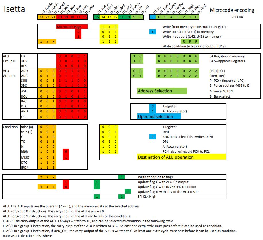
MICROCODE ENCODING
![]()
(The picture becomes slightly larger when you click it).
Some more details of the microcode encoding:
The main instruction type is determined by the 3-bit (yellow) destination selection.
An instruction can be in group 0 or in group 1. The group is determined by microcode bit 19 (ctl_alu3).
For group 0 instructions, the flag F can be written at the same time, with any condition, independent of the main instruction type.
Near the top of the overview, you see the instruction to write to the instruction register. You see that there is a 5-bit microcode page written, while the Isetta has only 16 pages of microcode instructions.
Normally, when writing to the instruction register, the next sequence will start at step 0 (from 16 steps). But when the lowest page bit (ctl_alu0) is set, it starts at step 8 of a sequence. So, when an instruction sequence is 8 steps or less, we can use the upper 8 steps for another 8-step sequence.The flag C (Carry) can written with an inverted condition. The main use of this, is write C with the inverted carry, to complement the carry flag. This was needed for the Z80, as described in this log . It is also used with condition 'bit0/' (bit0 of the result in the previous cycle) to write bit0 to the carry, together with a right-shift operation, to put the bit that was 'shifted out' into the carry flag. It can also be used to write C with a fixed 0 or 1 value.
There are two features for efficient reading from the SPI bus (for the onboard serial flash and the micro-SD card):
1) The ROL (rotate-left), instruction is used as a shift register to convert the serial SPI data to a parallel byte. Use the DPL register as source and also as destination for the instruction. But instead of shifting the carry into the byte, let the condition select the MISO signal from the SPI bus.
2) By making ctl_upd_c and ctl_wr_f both 1, the SPI clock will be high. This can be done at the same time as another instruction. But keep in mind that the value in C and F will be destroyed.
Together, these two features make it possible to read from the SPI bus with only two cycles per bit.The bankselect system is described in [this log].
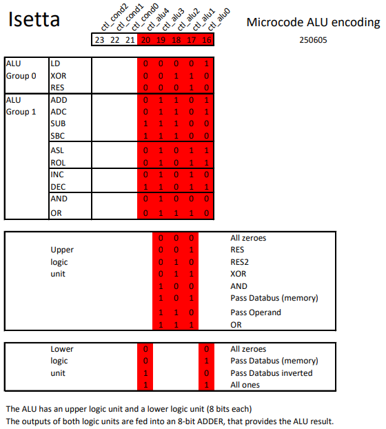
MICROCODE ALU INSTRUCTION ENCODING
The above picture gives an almost complete description of the heart of Isetta. But it does not describe the exact function of the five ALU control bits. So I describe that here:
![]()
The upper and lower logic units are described in project log #2. The control system has been a little simplified, but the principle is the same. The three control signals of the upper logic unit are the DCBA control signals, with the A signal always being 0. For the lower unit DCBA signals, B is equal to D and A is equal to C.
The function RES2 has not been discussed before. It is the same as RES, but with its operands swapped.
MICROCODE ADVANTAGES
When the program should run very fast, using microcode on Isetta helps a lot, because:
- The program counter can be used as second data pointer, eliminating many datapointer load instructions
- The T register can be used as second accumulator
- In a Z80/6502 program, only the hardware registers A and PCH/PCL are transferred from one instruction to another. But in microcode, all hardware registers A, T, PCH/PCL, DPH, DPL are available to the program.
- A Z80/6502 needs, for every instruction, a cycle to fetch the opcode from memory. These cycles are eliminated when programming in microcode. (a real Z80 takes even two cycles to fetch the opcode).
- By putting a selector value in the instruction register, CASE statements can be very fast
- In many cases, conditional jumps are eliminated due to the two-track microcode, so they take no time- In many cases, Z80/6502 instructions take cycles to write the flags correctly, even when these flags are not used. In microcode, you only have to write flags if that is needed for your program.
MICROCODE DISADVANTAGES
- The microcode is in parallel flash memory, and a programming device is needed to change it
- The microcode must check the interrupt-request signal regularly. This interrupt occurs every 400 cycles. It must always be serviced, otherwise the functions for screen output, keyboard and mouse input will not work correctly (But checking the interrupt request can be done in zero cycles).
- Not very memory efficient. A micro-instruction, on its two 'tracks', takes 6 bytes (2 x 24 bits). And several micro-instructions might be needed to do the work of a single Z80 or 6502 instruction.
INTRODUCING THE BLITTERAfter glorifying the microcode, it won't be a surprise that I wrote screen functions in it.
The Blitter (Wikipedia) is a microcoded unit that is specialized in writing to rectangular sections of the Hires screen.
To use this, you first setup the parameters, using special OUTPUT ports. After that, you start the blitter by writing the action code to the P_BLITCTRL output port.Most commands require three kinds of parameters: (most parameters are 16 bits)
- memory source base address, coordinates, line-length
- screen coordinates
- rectangle size
A few commands use FILL1 and FILL2 that both specify a color.The Blitter supports the following actions (not all of them fully working yet):
D_BMCOPY ; COPY source to screen
D_BMCOPYCNV ; COPY source to screen, converting SymbOs color numbers to Isetta color numbers.
D_BMSKIP ; Copy source to screen, except where source has color 0 (transparent)
D_BMSAVE ; Save from screen to source memory address
D_BMTEXT ; TEXT write a character from a font map to the screen. Font map is 1bpp.
D_BMFILL ; Fill a screen rectangle, alternating colors FILL1 and FILL2 (in most cases they are the same)
D_BMFXOR ; Fill a screen rectangle using XOR operator, alternating colors FILL1 and FILL2Most of these use the format of two 16-color pixels per byte (4bpp).
The COPY and SKIP will possibly also support four 4-color pixels per byte (2bpp) as source.The blitter is fully described in the Isetta Hardware Manual, that you can find it in the File Section.
MOUSE
I also have more code for the mouse now... I have a mouse pointer on the screen, that I can move with my mouse (Taken for granted nowadays, but it will not work without hardware or code that implements it).
Before the mouse pointer graphic is placed, a D_BMSAVE is used to save the background. Then, the mouse pointer is copied to screen using D_BMSKIP.
When the mouse is moved, the background is restored with a D_BMCOPY action, and then the mouse pointer is placed at the new position.OK.... you can conclude that I didn't spend a lot of my free time watching TV.
Isetta TTL computer
TTL Retro computer runs 6502 and Z80 code. Has video, sound and filesystem. Runs a Windows-like OS. No microprocessor or FPGA.