 Chris
Chris-
Battery Mystery Solved (and more wire bonding by hand)
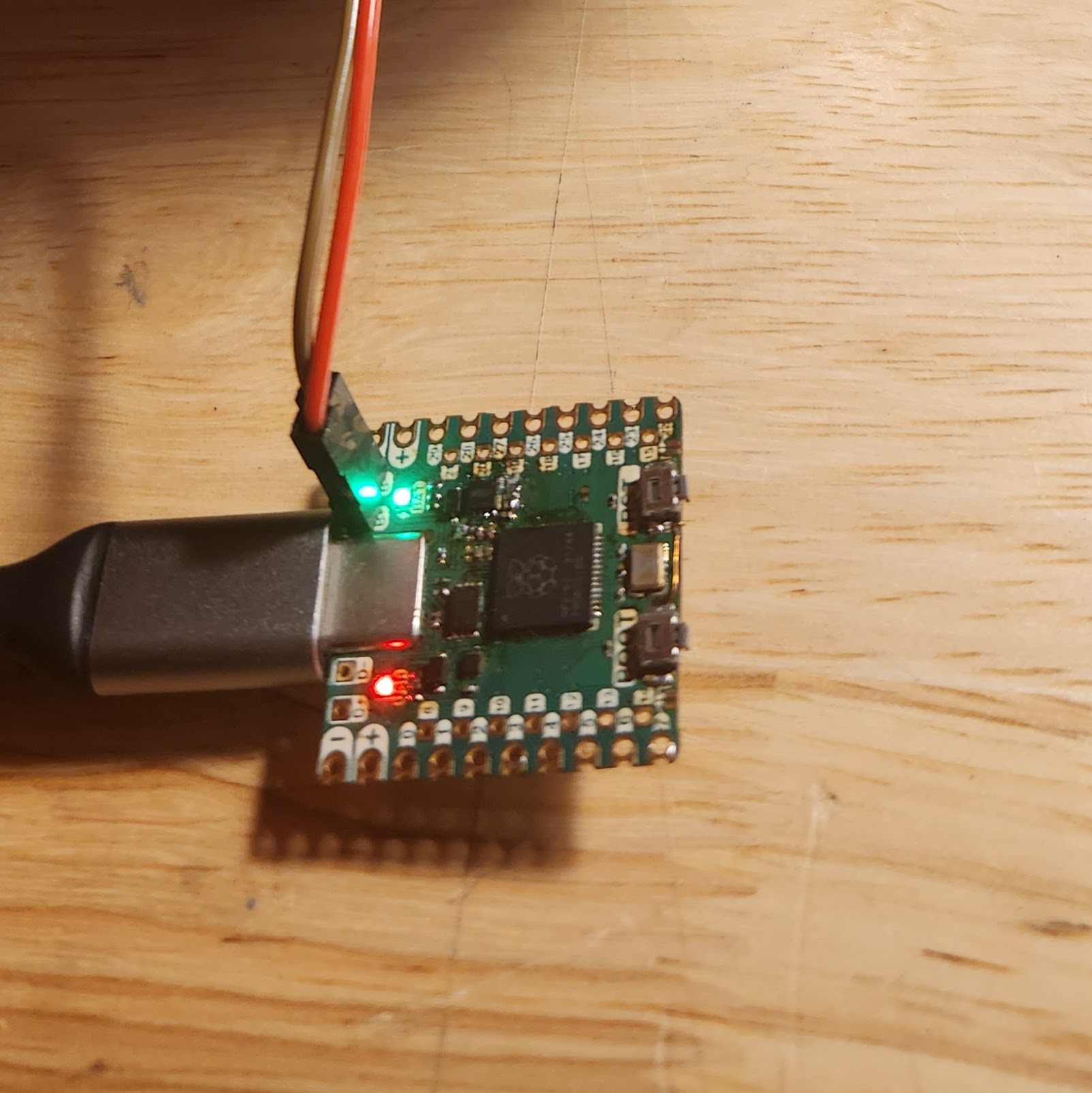
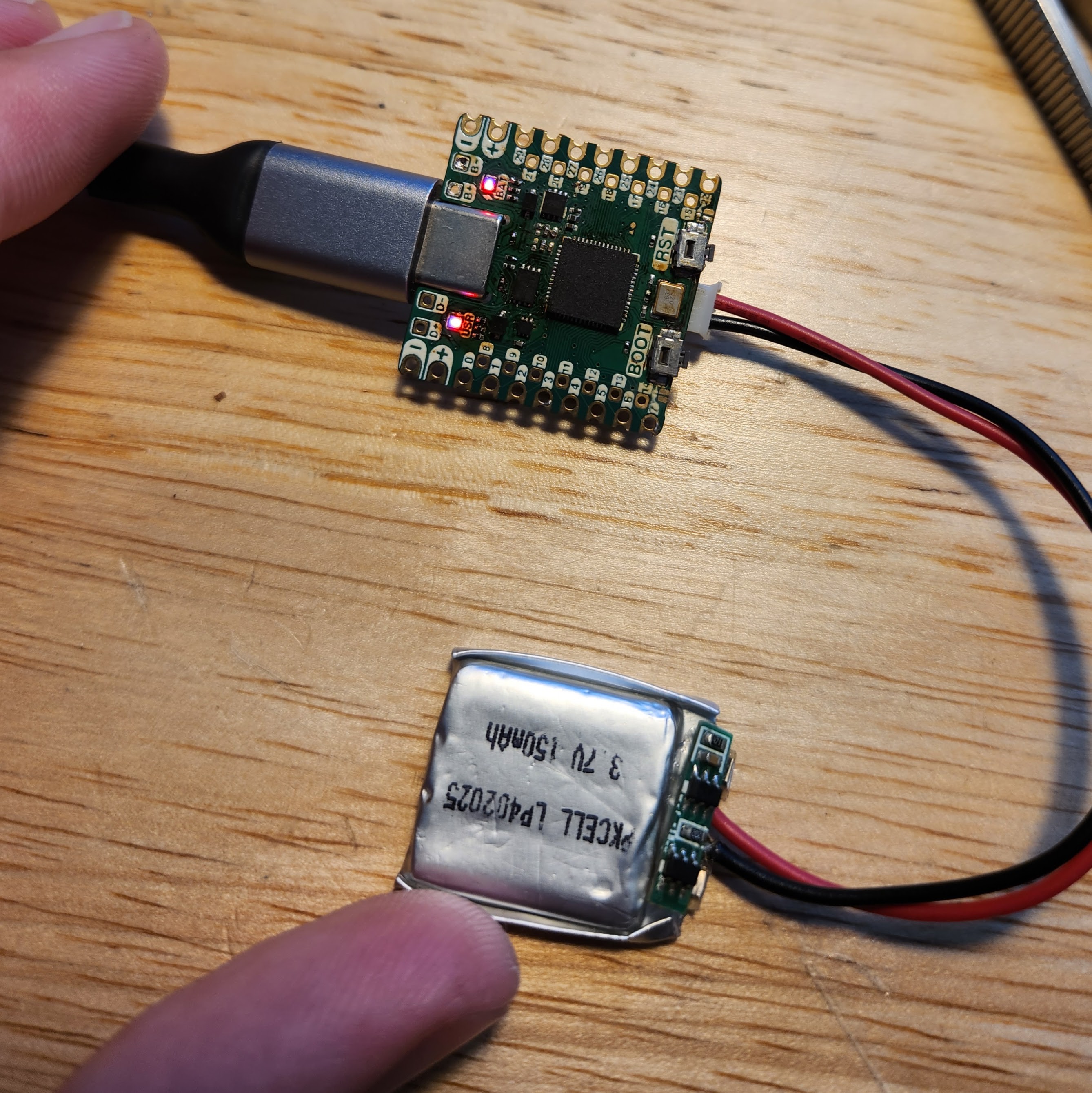
01/29/2024 at 01:21 • 0 commentsA short log with lots of eye candy, but perhaps one of the most triumphant logs yet! In short, I have had trouble with my charging IC for the past few months. First, it wouldn't charge all the way, and the light would remain forever red. Second, it would stay green (reporting fully charged) even with no battery connected. This is undesired behavior which was not present on Rev. 2 of the boards, which only suffered from the former issue.
I realized that if I want the DONE and CHRG light to both remain off while there is no battery connected, I need to remove the suggested capacitor at battery input.
![]()
I guess it makes sense that the chip behaves this way. From what I can tell, the IC is essentially charging the capacitor to a little over 4V and then reporting DONE. Based on some probably erroneous calculations, the capacitor is being charged at about 3 uA and has a DC impedance of about 1.32 MOhms.
This chip does have a low current "trickle charge" meant to revive dead cells. It's possible that 3 uA is enough for the chip to operate in that regime and enable it's constant current supply into the capacitor.
Either way, I get my desired behavior when I remove the input capacitor. This seems like a bad idea, because it is. Without this capacitor, the CHRG and DONE light flip out when I press my finger to the contacts while the battery is disconnected and who knows what sort of instabilities that could lead to. I wonder if I can just use a TVS diode to kill any transients. I found a 0201 TVS diode with a leakage current of just 0.2 uA. Maybe that will be low enough as to not trigger the charging IC while still providing some transient protection.How did I figure all of this stuff out? I breadboarded! How do you breadboard components that could fit through the eye of a needle? Just check out the pictures below...
![]()
![]()
![]()
![]()
-
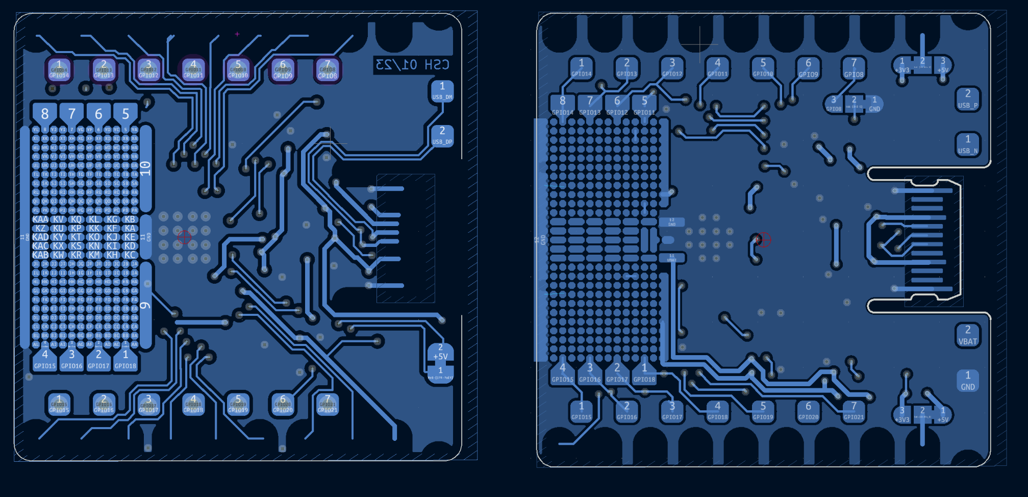
CRAPi Rev. 3 is Complete (thank you PCBWay)
11/28/2023 at 04:47 • 2 commentsThat's right, Rev. 3 is basically complete and the board is almost ready for public consumption! There are a few different changes that I will get to but first:
A huge thank you to PCBWay for sponsoring this run of pcbs!While PCBWay sponsored this revision of the CRAPi board, all of the following opinions are my own.
A rep from PCBWay reached out to me after my last post and thanks to his incredible generosity I was able to check out their services. I had never used PCBWay before so I didn't know what to expect, but right off the bat I noticed that the customer service was impeccable. They have a great intake system that let's you correspond with the representative responsible for your boards directly from within the website (as opposed to an email chain). My absolute favorite part of their website was the real time tracking of the PCB production stages. It's really cool to know exactly what stage of the production process your board is in and know when progress is being made.
Really the only negative aspect (which isn't really negative at all) of the proofing process was the final cost/capability assessment. PCBWay takes a very professional approach in their proofing process and if you mis-specify your required manufacturing capabilities (trace width, drill diameter, etc.) they will ensure that those specifications are corrected and that your PCBs match your gerbers as closely as possible. This is in contrast to my experience with JLCPCB, who simply approved my design and sent it off for a best effort approach on their production line, resulting in different via diameters and trace widths than what I specified in my design.
The proofing process resulted in a significant increase in the cost of the boards which was a bit shocking. Given that these boards were sponsored I choose to proceed with their recommended process specifications but in the future I would most likely work more closely with my representative to strike a balance between cost and specifications. It's clear that there is just a higher level of professionalism with PCBWay!
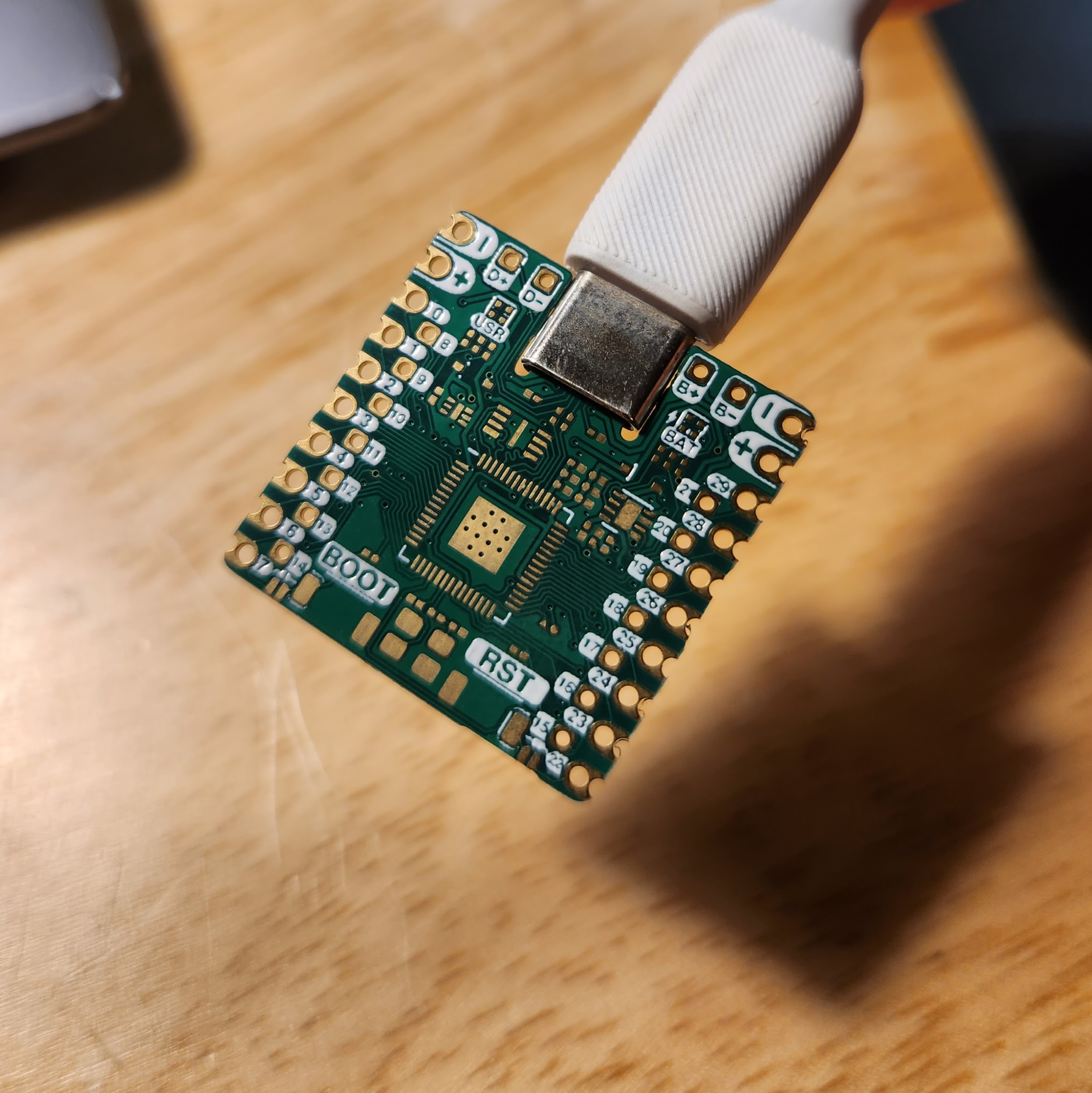
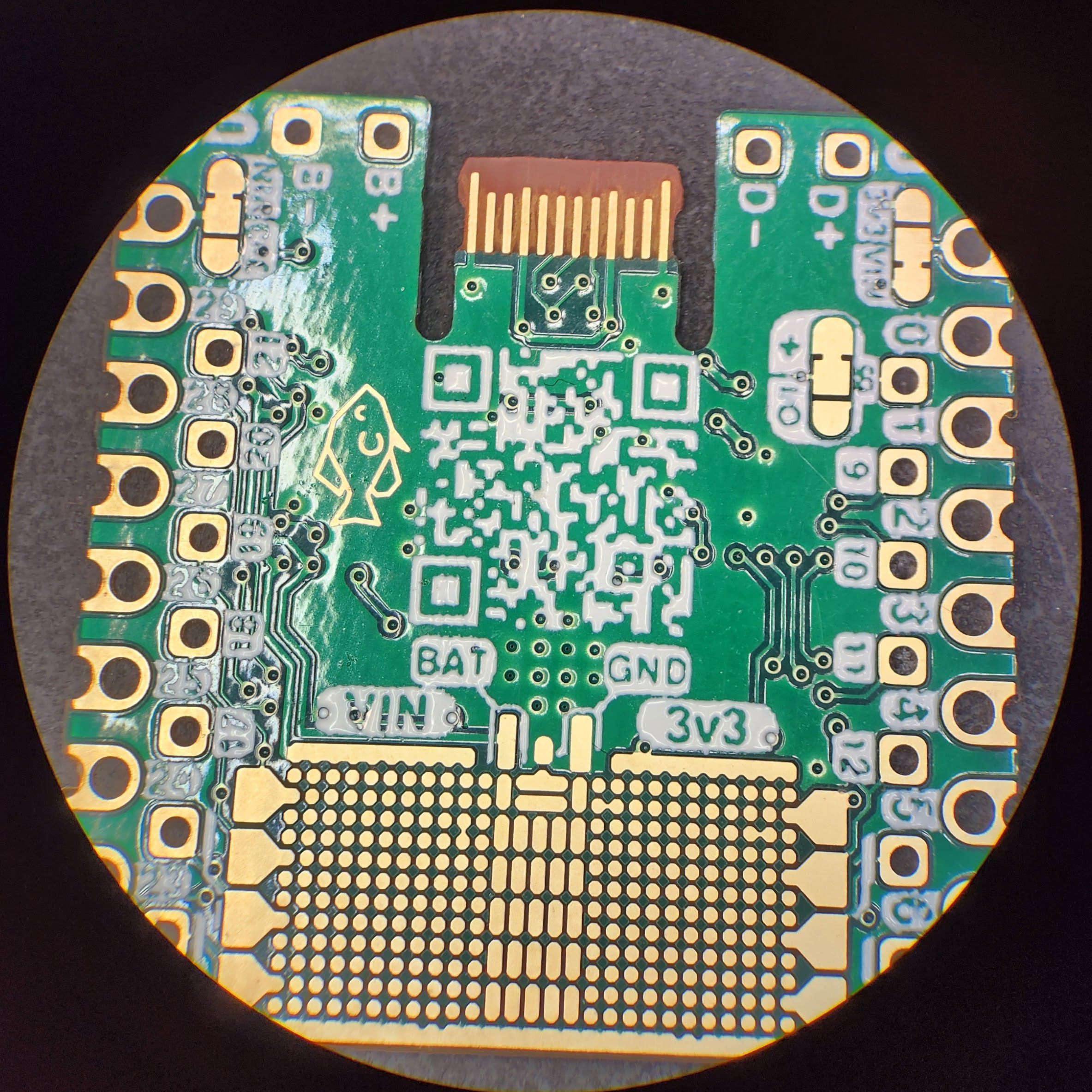
Once that boards were done they arrived via DHL in just a few days. Incredible! I think they turned out very nicely.![]()
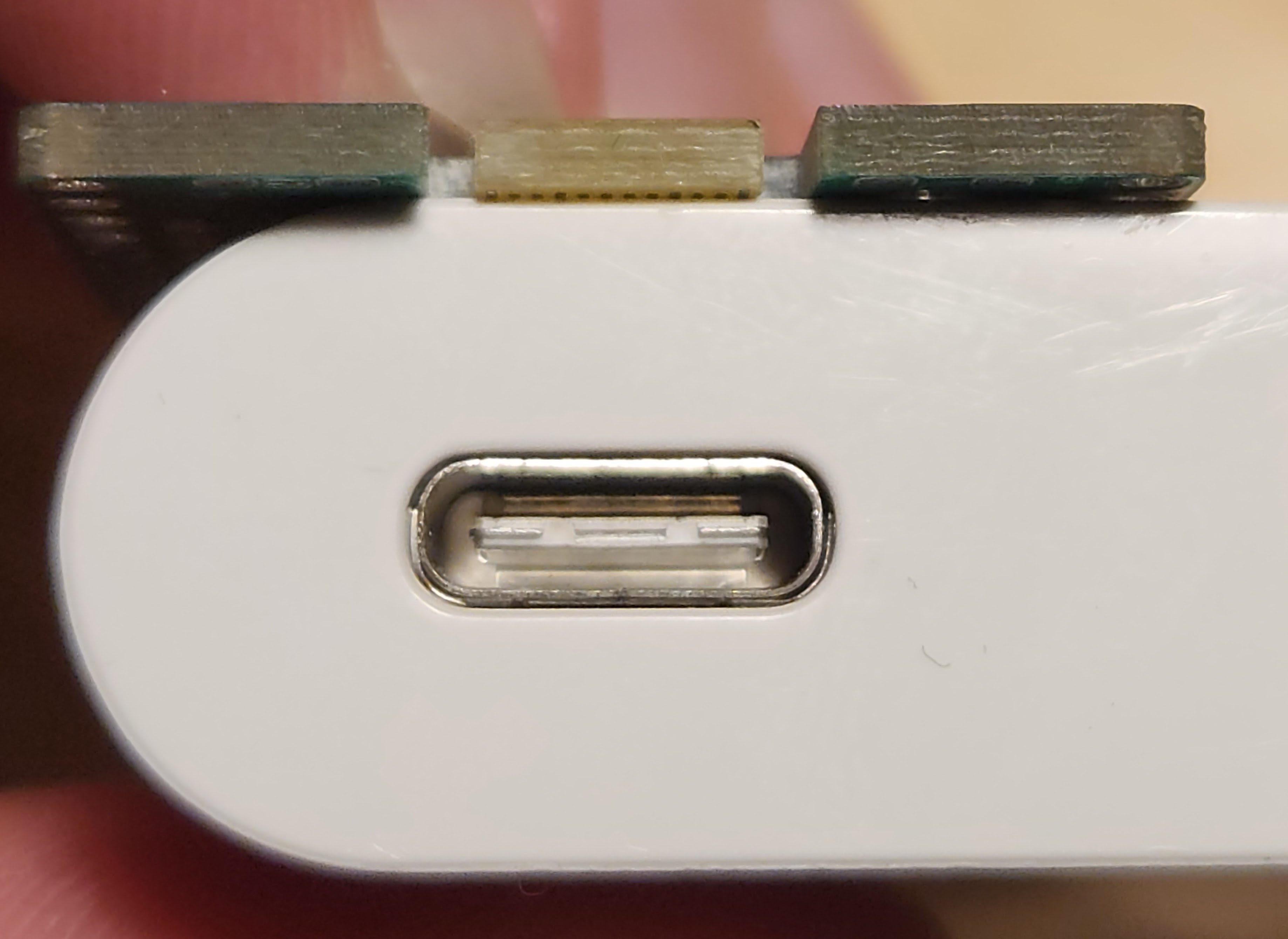
This time around I was curious about how the thickness of the PCB would effect the retention force of the USB connector. The green boards are the 0.6 mm that I have used for the previous revisions and the blue board is 0.8 mm. The USB-C specification is 0.7 mm. The blue boards were almost impossible to disconnect accidentally. The force required to unplug it was almost too high. It also appears that the contacts on the blue board slowly get mushed down after repeated connections. I need to do some more repetitive testing before I decide on a final thickness and weight the costs and benefits of the thicker board.
![]()
PCBWay also did a superb job routing the small detents into the side of the USB-C connector. Previous revisions that used the JLC boards were far less crisp and the increase in quality is evident in the improved retention force of even the 0.6 mm thickness.
![]()
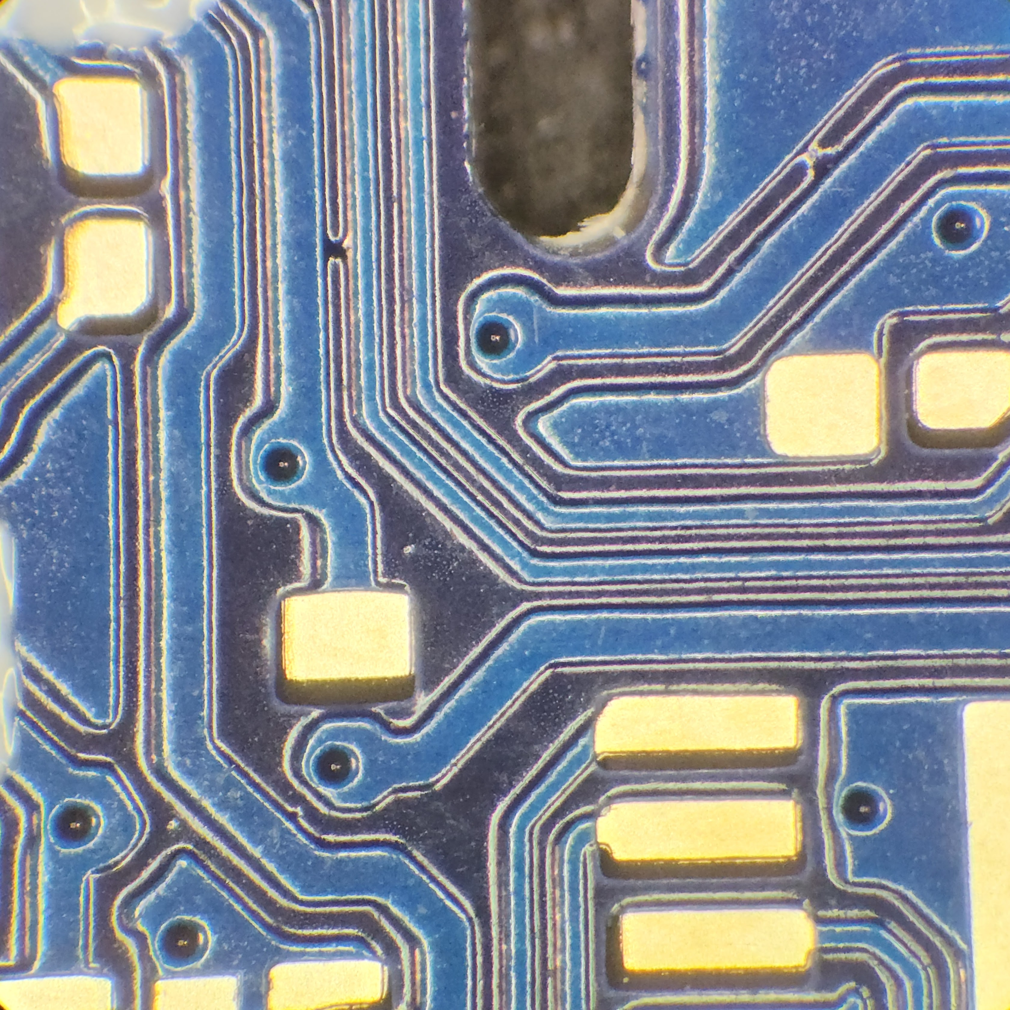
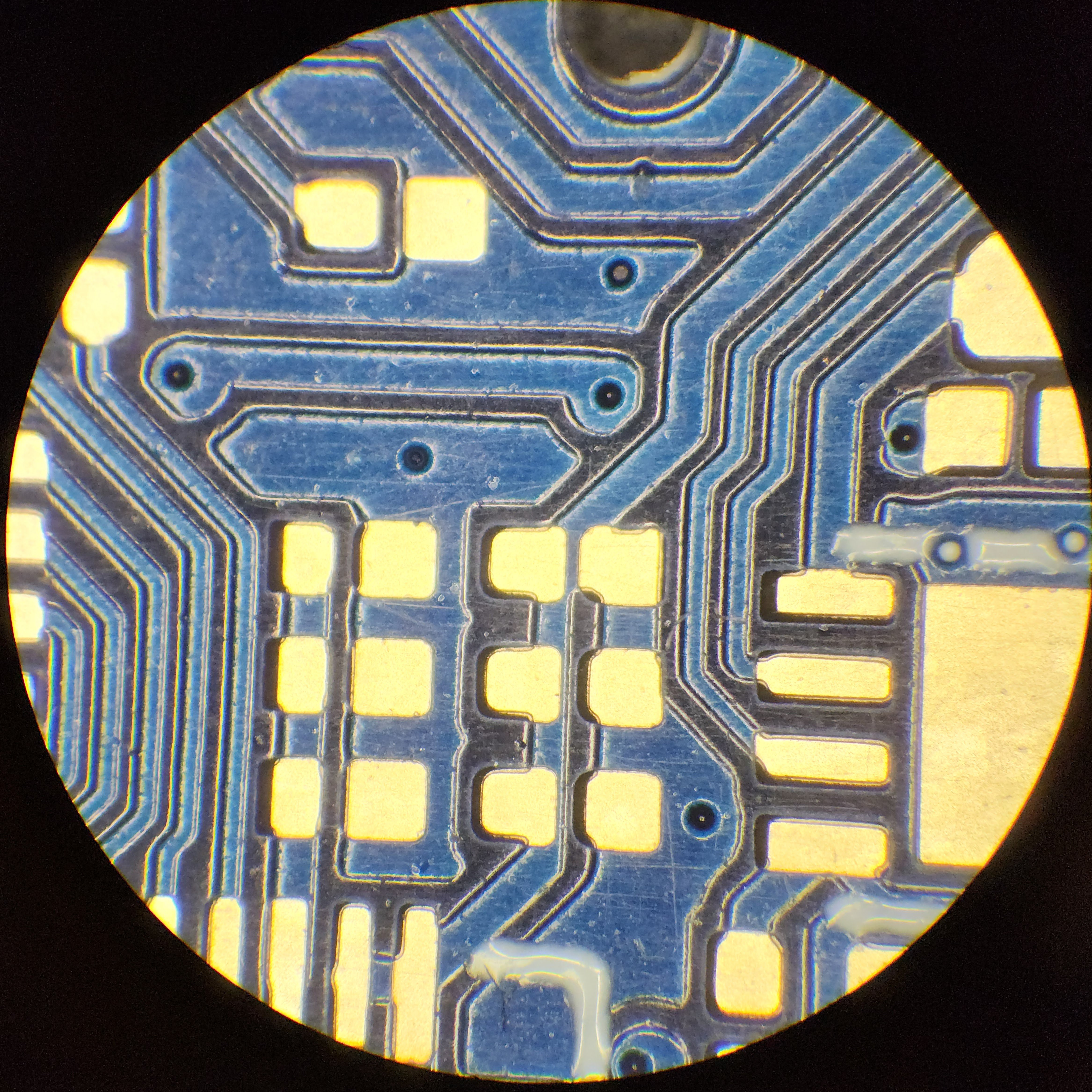
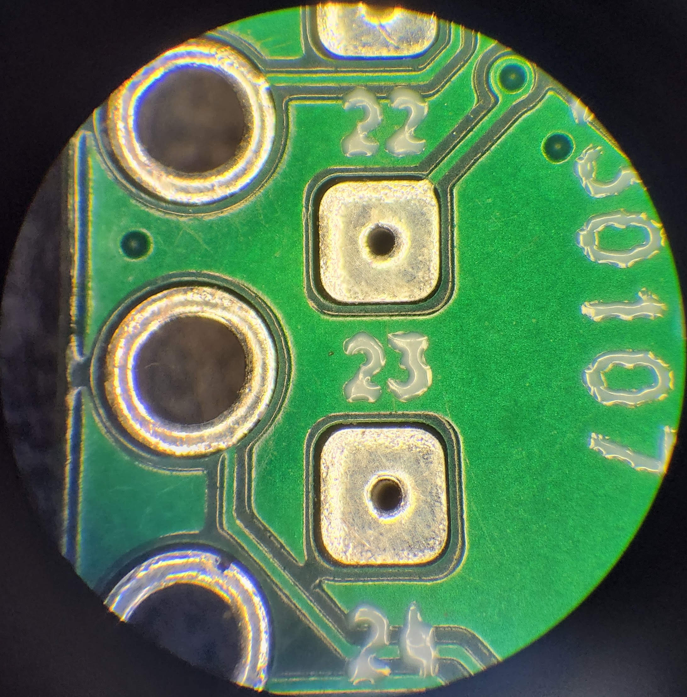
Really the only criticism of their build quality was a slight mismatch on the registration of the vias. The vias uniformly off-center from their desired locations across the entire PCB. It's quite possible there could have been an issue with my gerbers, or that I am simply pushing the limits of their production capability. Nevertheless, they were all consistently covered with soldermask and this slight registration mismatch didn't cause any problems.
![]()
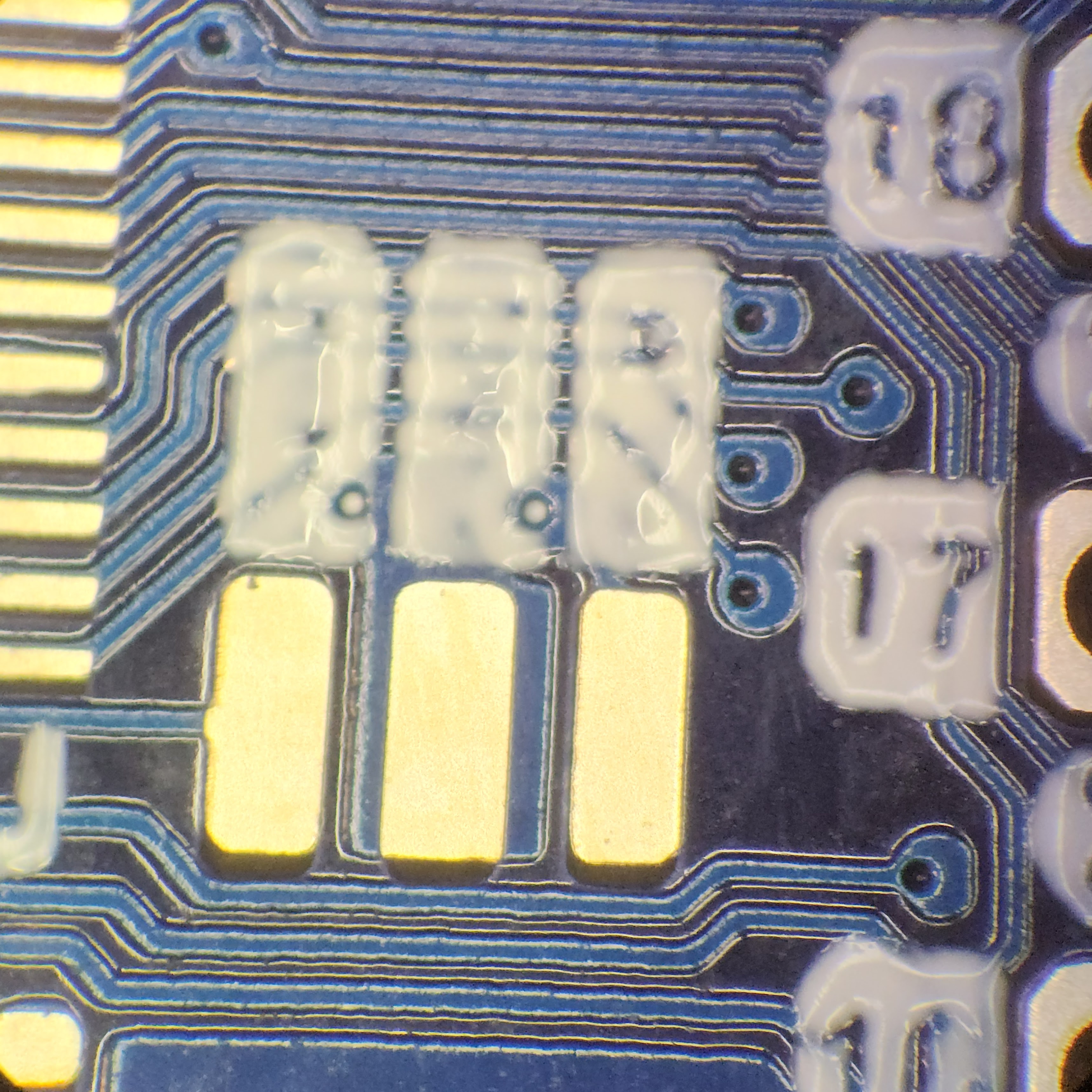
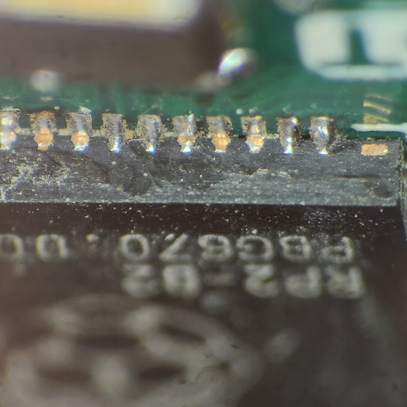
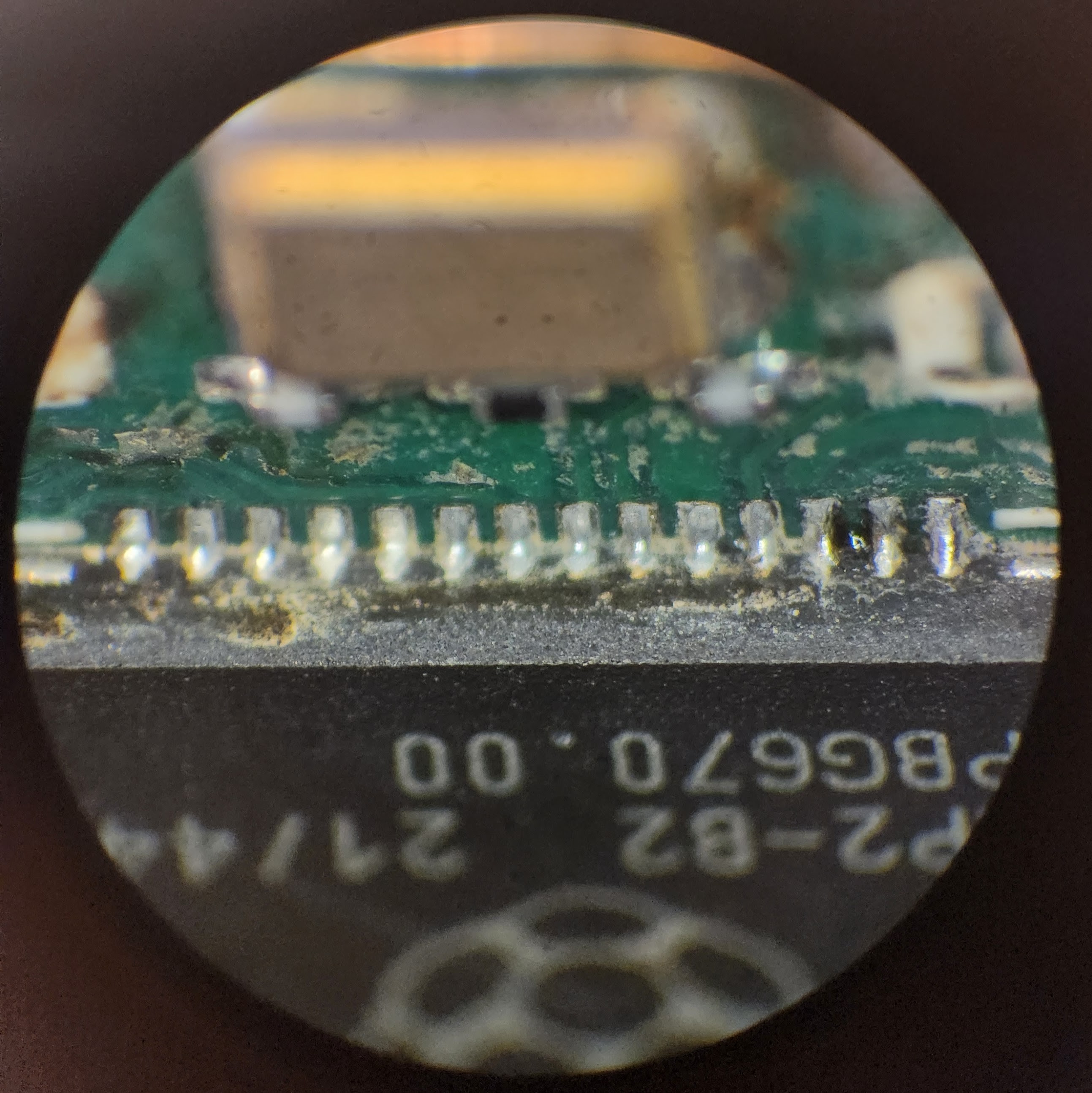
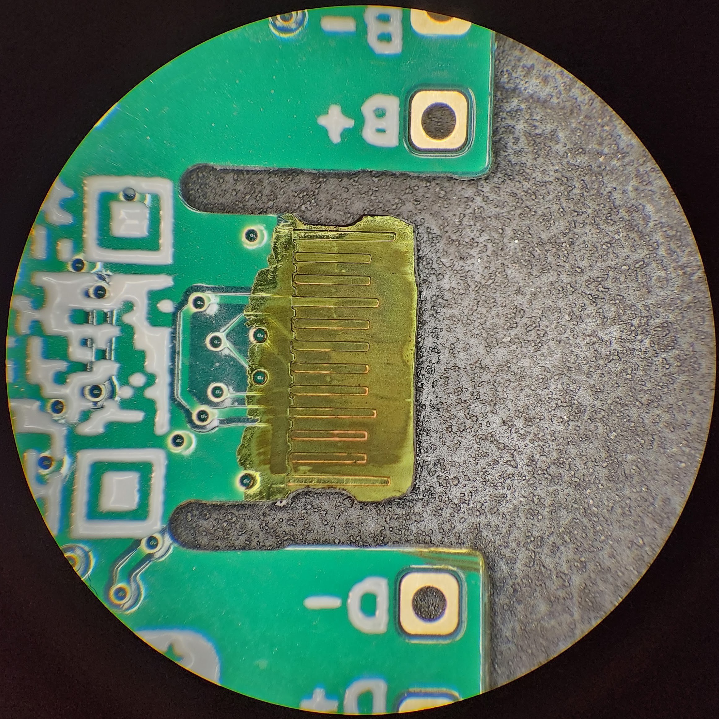
I was curious about the quality of PCBWay's silkscreen. I didn't have expectations because I am working at the limit of the typical liquid photo imaging (LPI) silkscreening process. Next time I order PCBs I am going to make sure to select the direct legend printing option so that all my labels can finally be read. That option is a flat 80 dollars so unless I am ordering a bunch of boards it hasn't been worth it, yet. The legends below are supposed to be labeling the debug header...
![]()
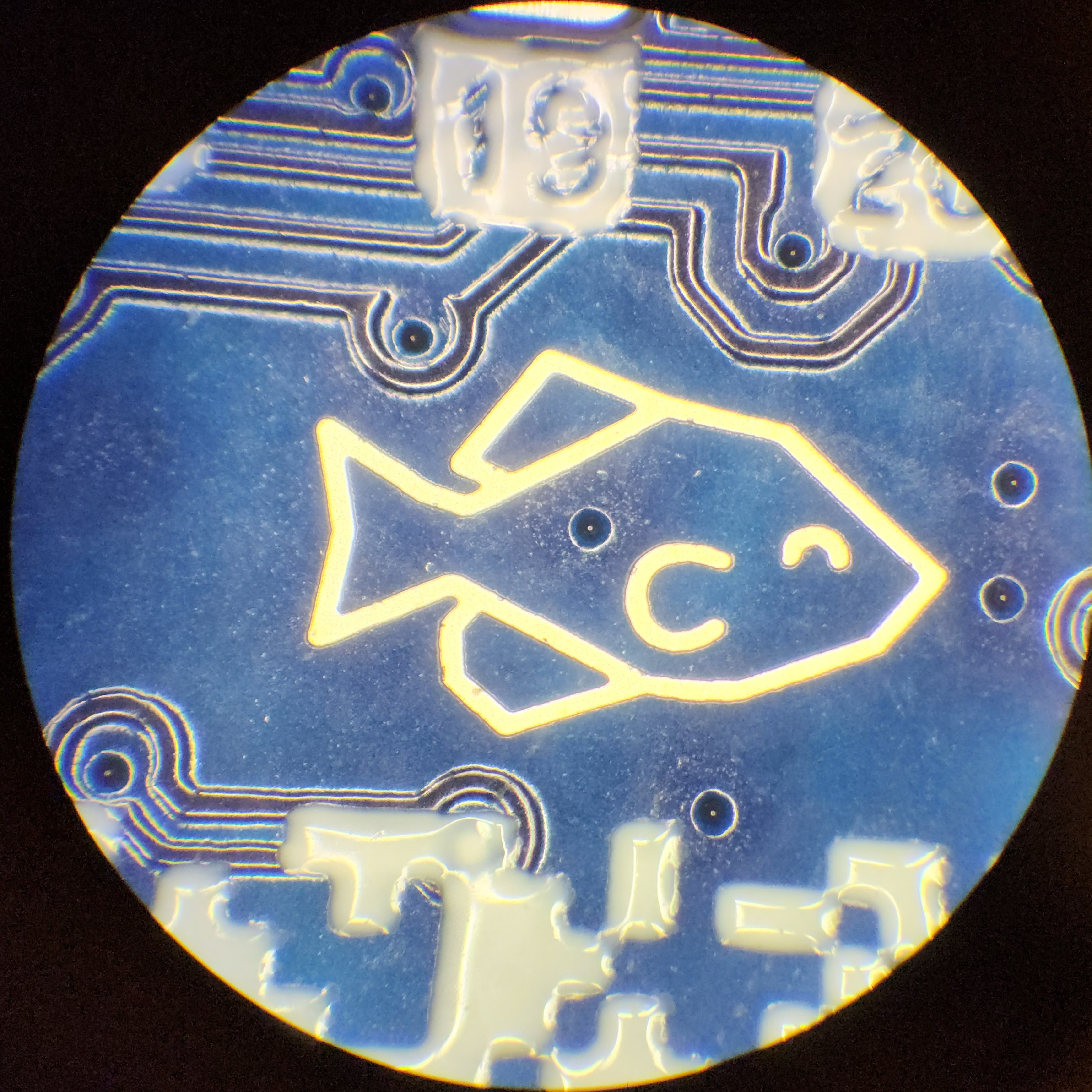
The solder mask capability on the other hand is impeccable, as expected. Look at that happy little crappy!
![]()
So overall I am very happy with the quality of the boards that I received and of course I would like to extend a huge thank you to PCBWay, again. I will definitely be ordering from them in the future and I encourage you to check them out. I plan on selling these boards so I am also very interested to trying out their PCB Assembly service.
What changed and where are we now?
There were a few major changes that came along with Rev. 3:
- A better Protogrid
- 20 mil spacing is much more usable and targets SOIC-8 packages
- Larger pads that wont fall off and are hand solderable
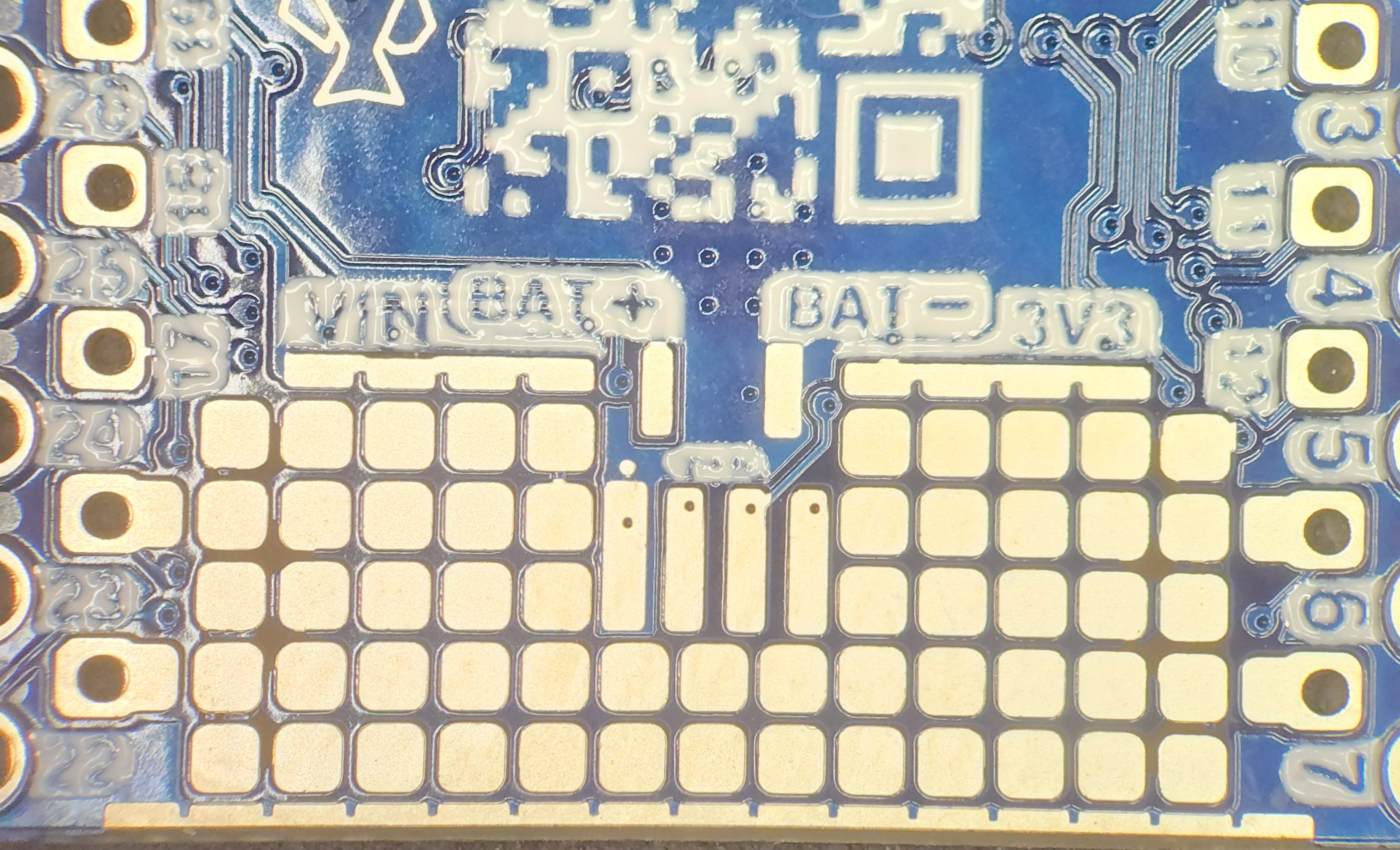
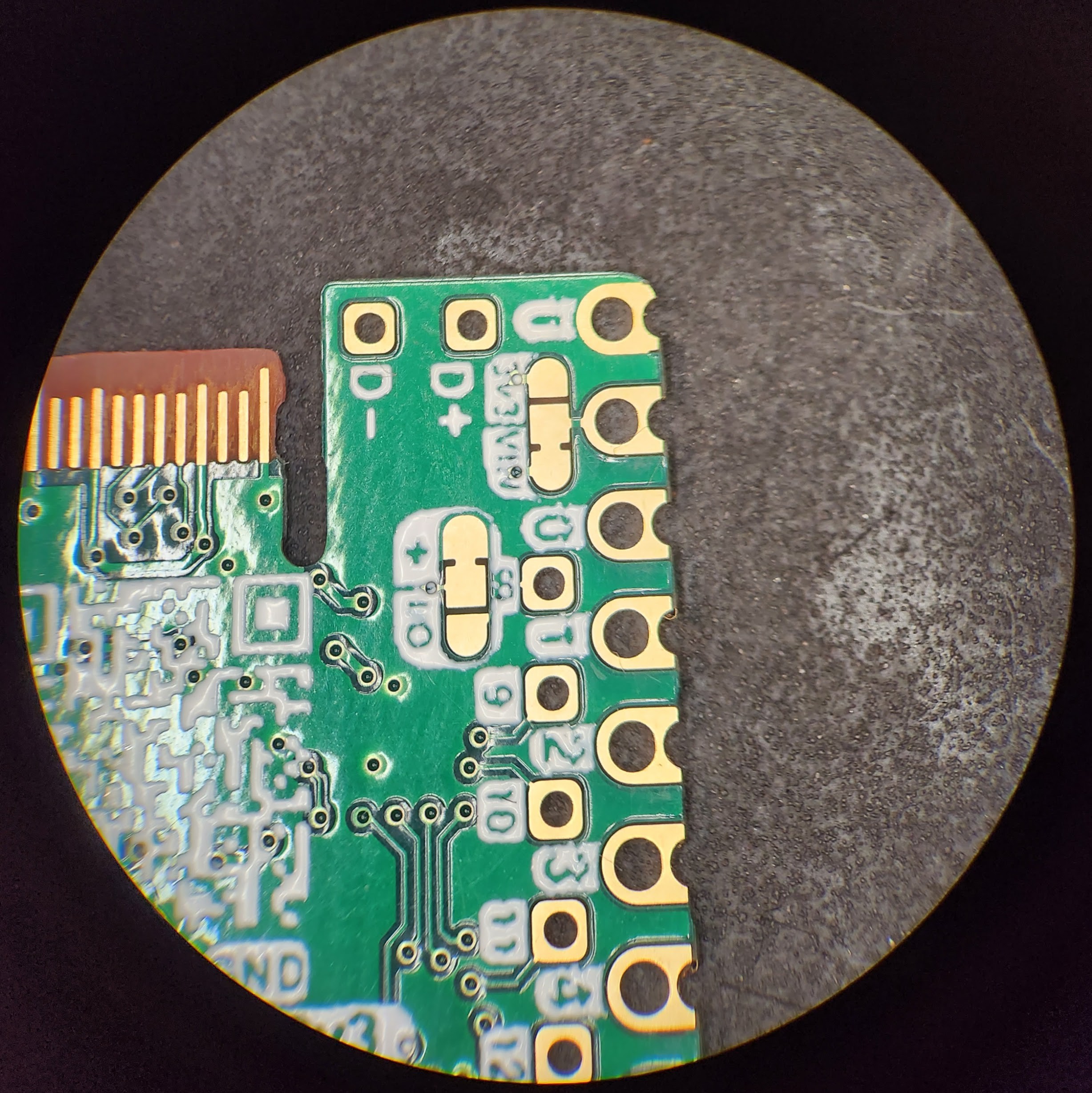
- A Qwiic connector foot print
![]()
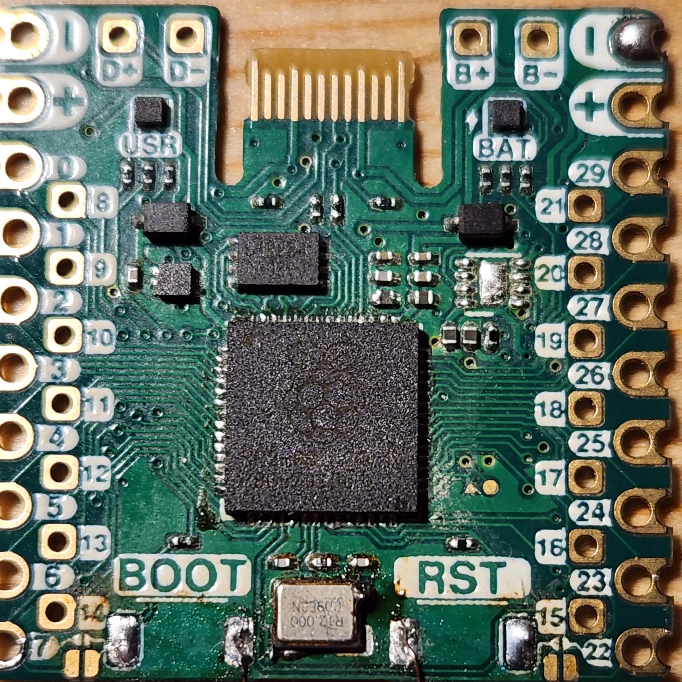
- Raspberry Pi Pico compatible debugging foot print
- I managed to jam in the same footprint that the Pico uses for the debugging port, which makes this board compatiable with the Raspberry Pi Debug Probe connectors.
- An improvement of the two tiny little testpoints I had before.
![]()
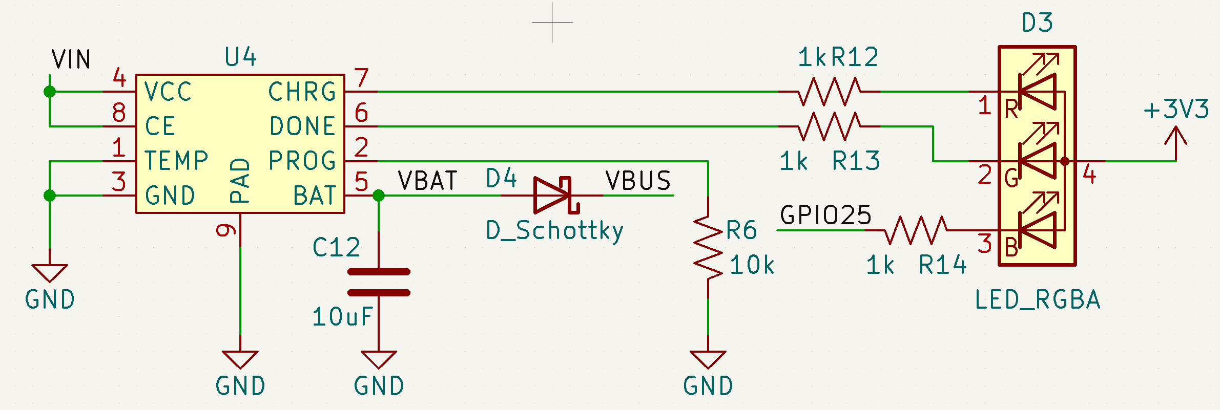
- More efficient power switching / battery charger
- The addition of a P-FET in an ideal-diode-like configuration means we are dropping a fraction of the voltage we were with the previous schottky-based approach.
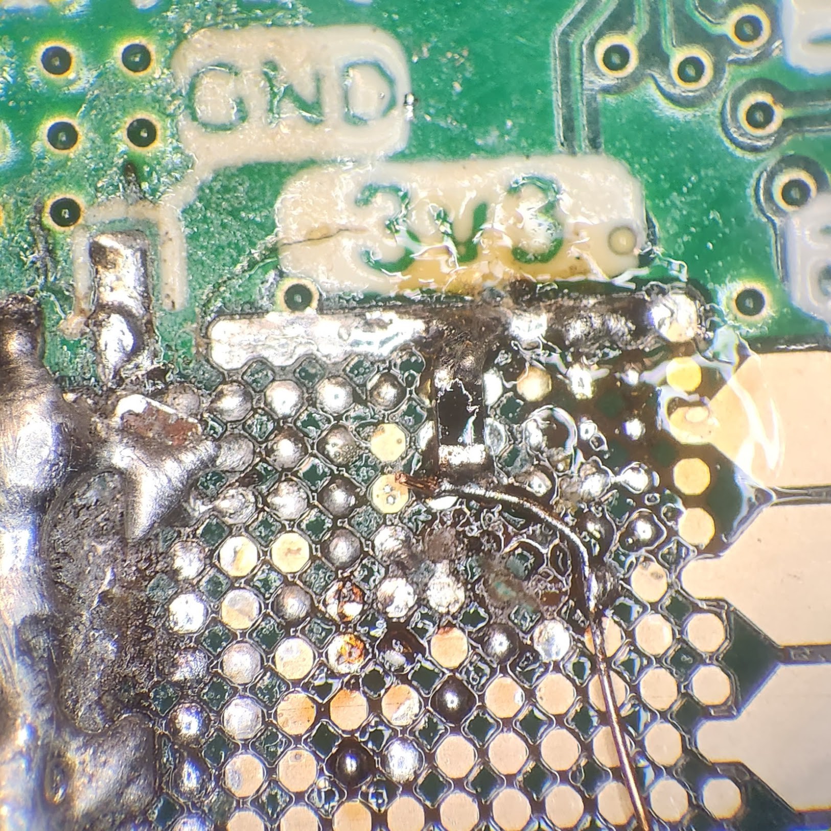
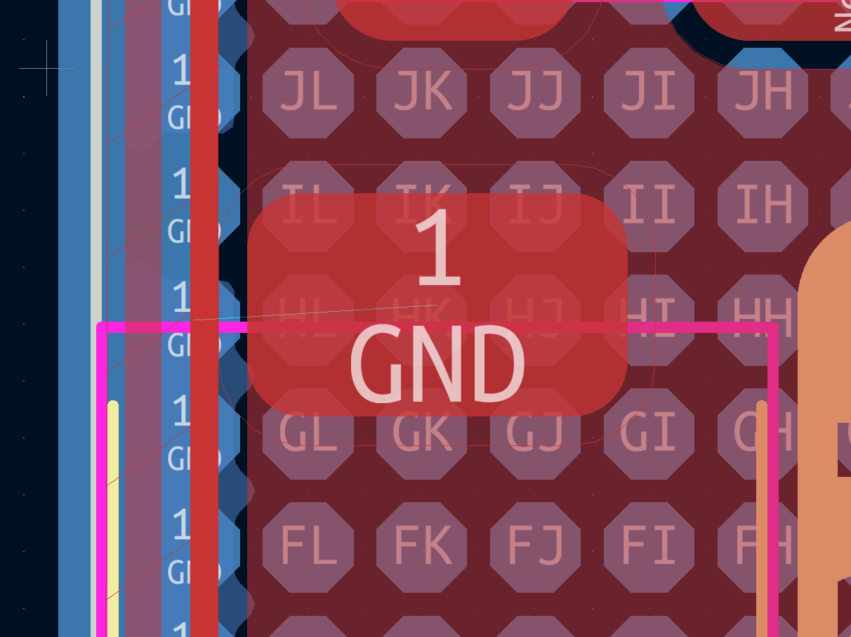
I think the next spin of the boards should be ready for public consumption. I did have one major mistake because I forgot to re-enable some DRC settings and accidently shorted 3.3V to ground. Some quick work with a razor took care of that though. At least it's an easy fix!
![]()
![]()
As this project enters its second year I want to thank everyone who has been following along. Sometimes it feels like we are asymtotically approaching completeness but I think the end is in sight!
- A better Protogrid
-
(Feels Like) Wire Bonding By Hand
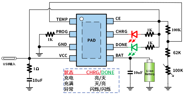
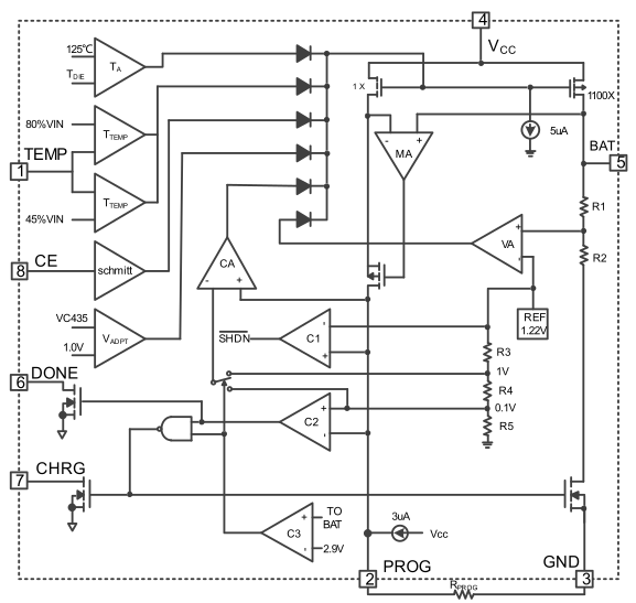
10/08/2023 at 20:03 • 5 commentsI think I finally figured out my LiPo Charging woes! As a reminder, the LiPo IC would not fully charge the connected battery when a Schottky diode was present at the LiPo's output. This diode allows the CRAPi board to switch between USB and battery power with minimal fuss.
I figured adding a LiPo charger would make the CRAPi board way more useful, plus it would help fledgling dev board give the big boys a run for their money. Looking at you Adafruit and Pimoroni.
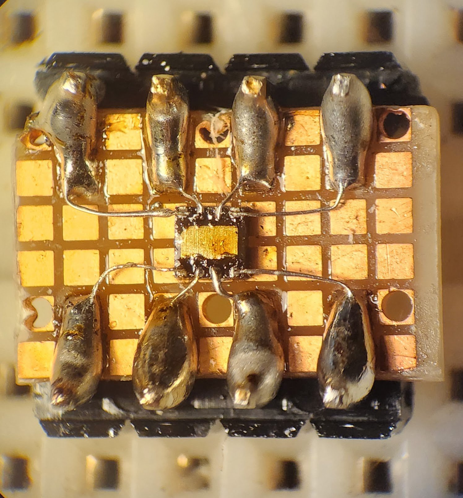
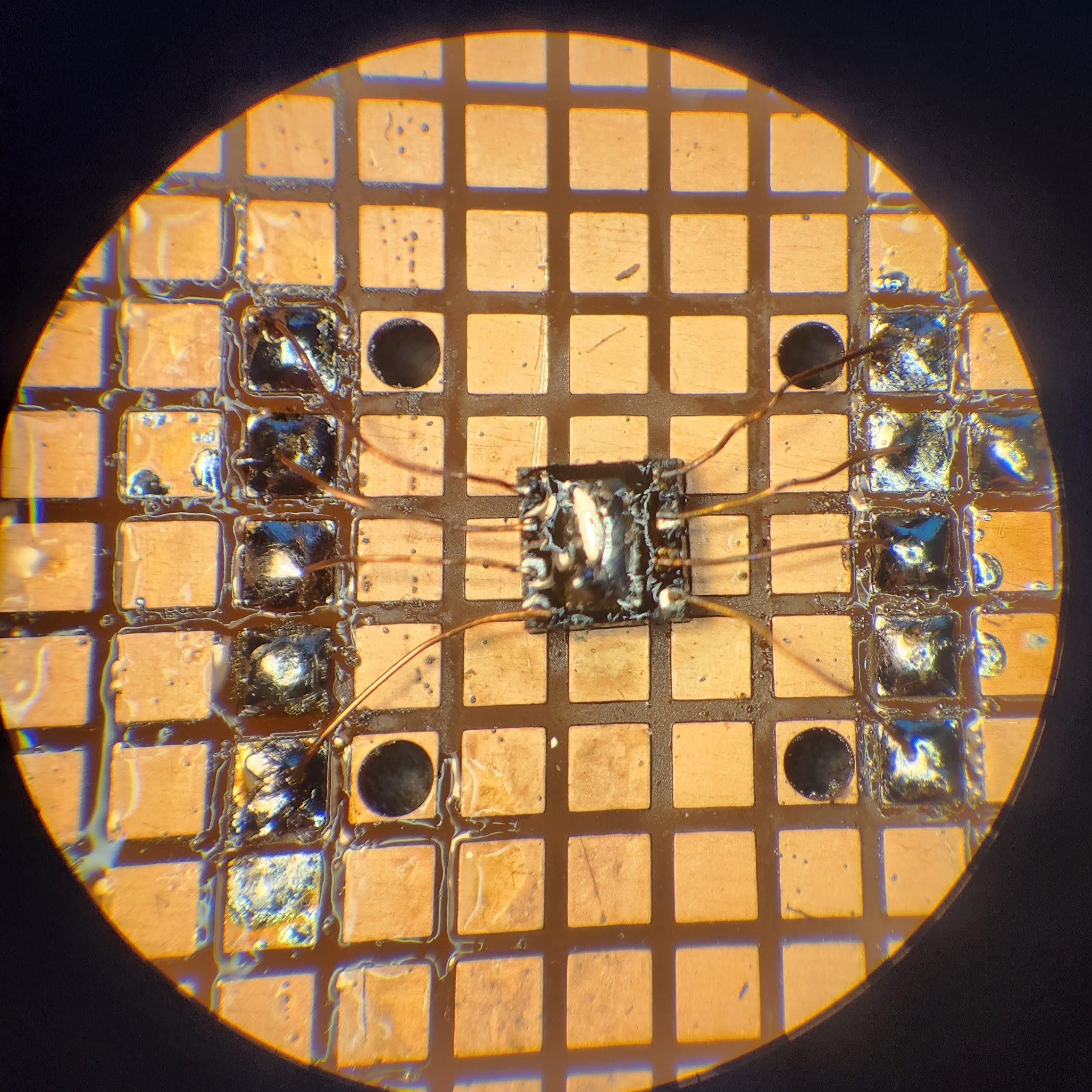
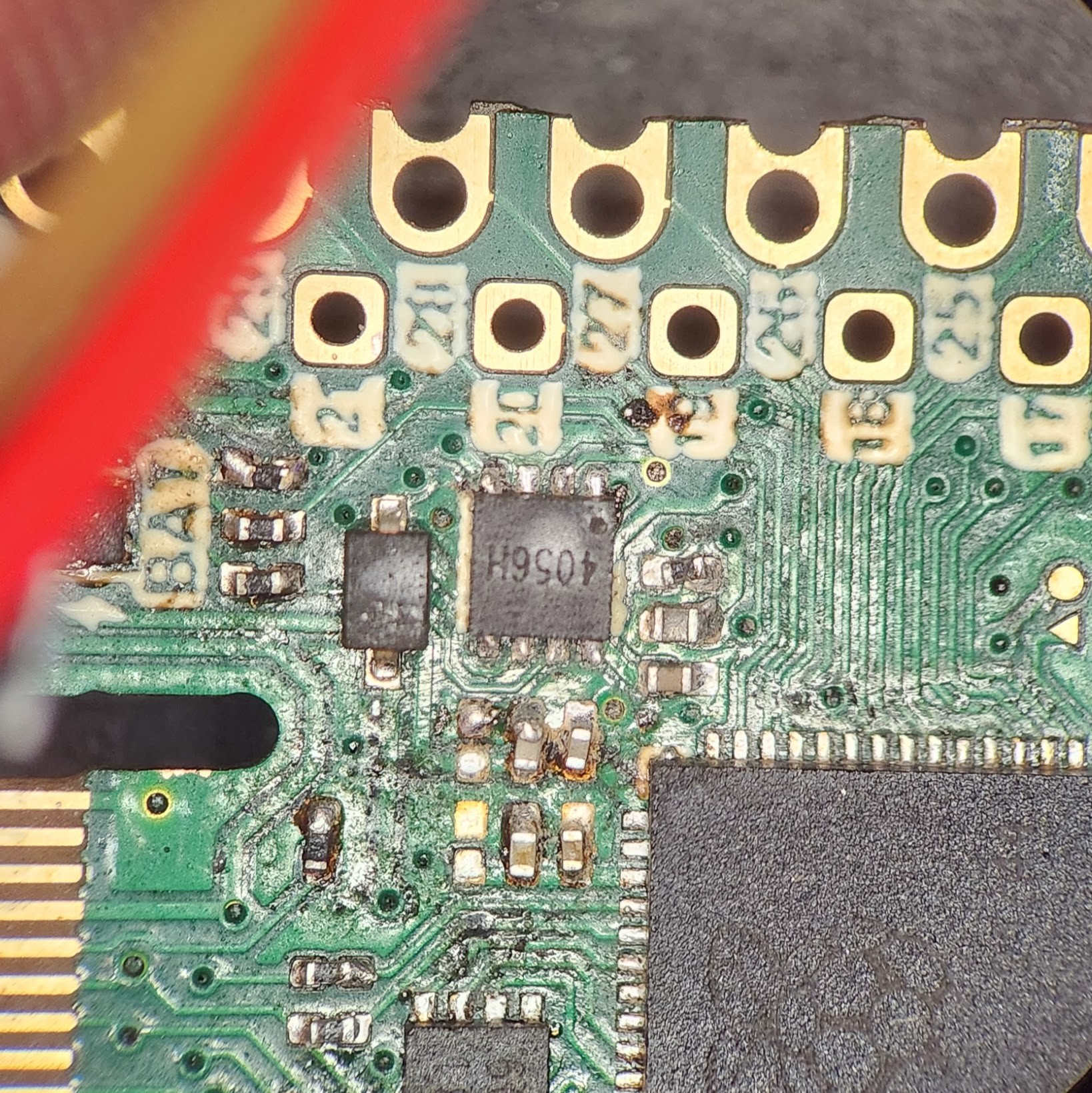
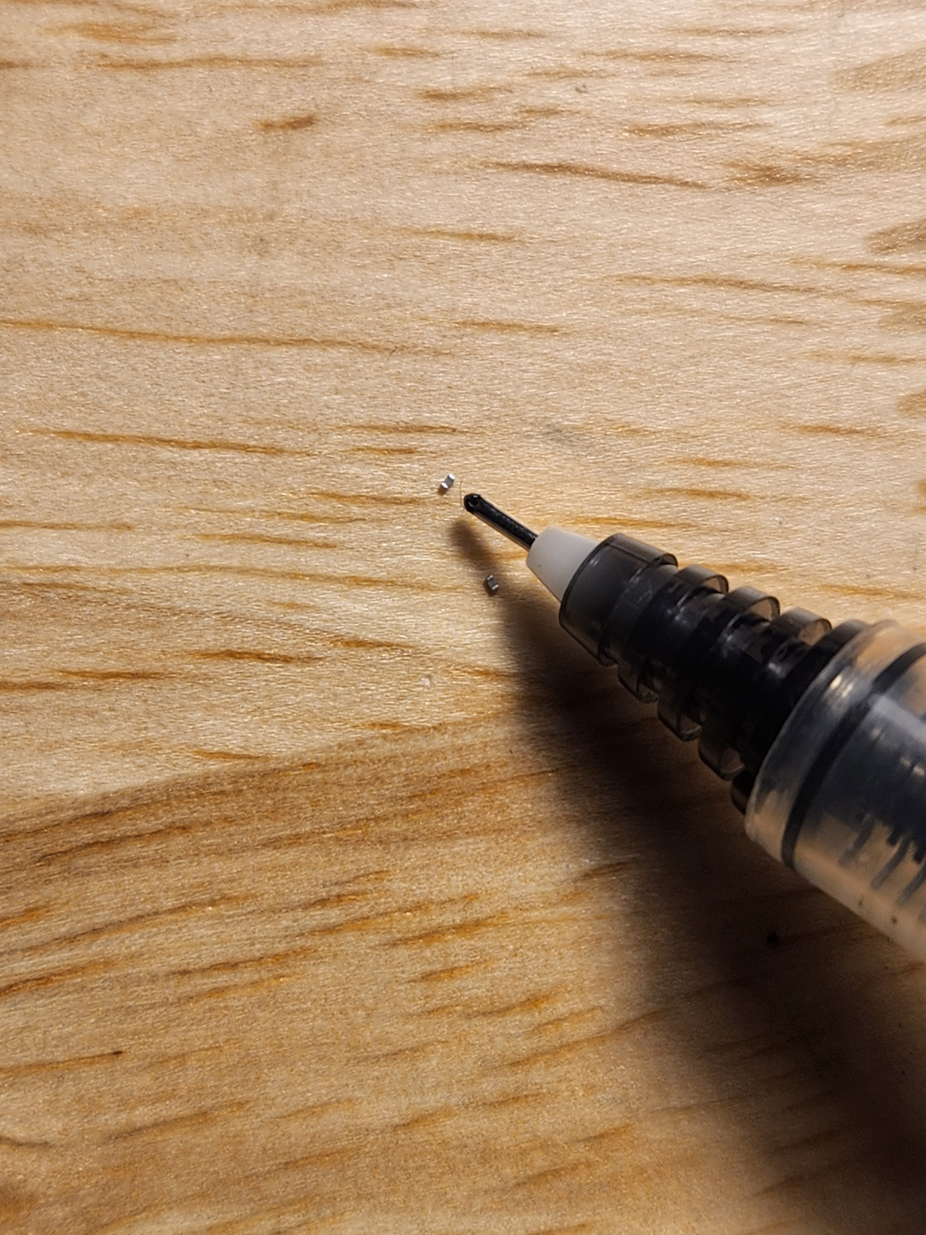
This was supposed to just be another IC and a few passives. Instead, I ended up dead-bugging a chip measuring 1.5mm x 1.5mm. With the hope of troubleshooting the circuit directly.
Yep. Check out the picture below. It really did feel like wire bonding!
![]()
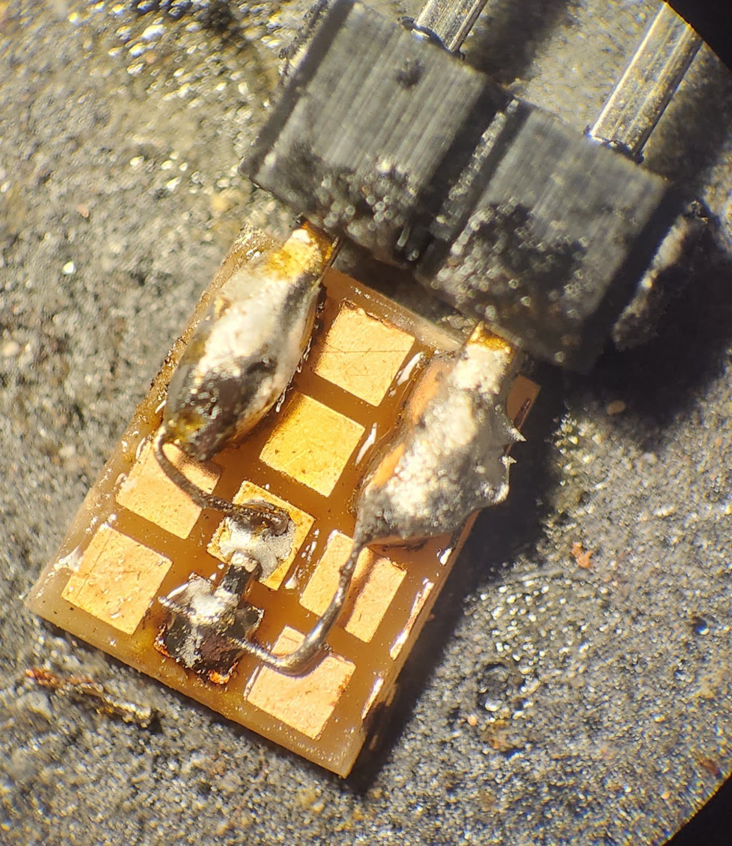
The copper wires are once again the strands from those cheap jumper cables. They are super thin and readily accessible. Unlike magnet wire, they don't have any insulation on them which I like. It means that I don't have to mess around burning varnish and the crust that comes with it. There isn't really much of a danger of shorts either, the wire is so thin that you can just route it around in midair and it stays put.Here is a partial picture of the completed circuit. After the strong start with just the chip I was a little disappointed I couldn't do a better job on the rest of the circuit but I didn't have all night...
![]()
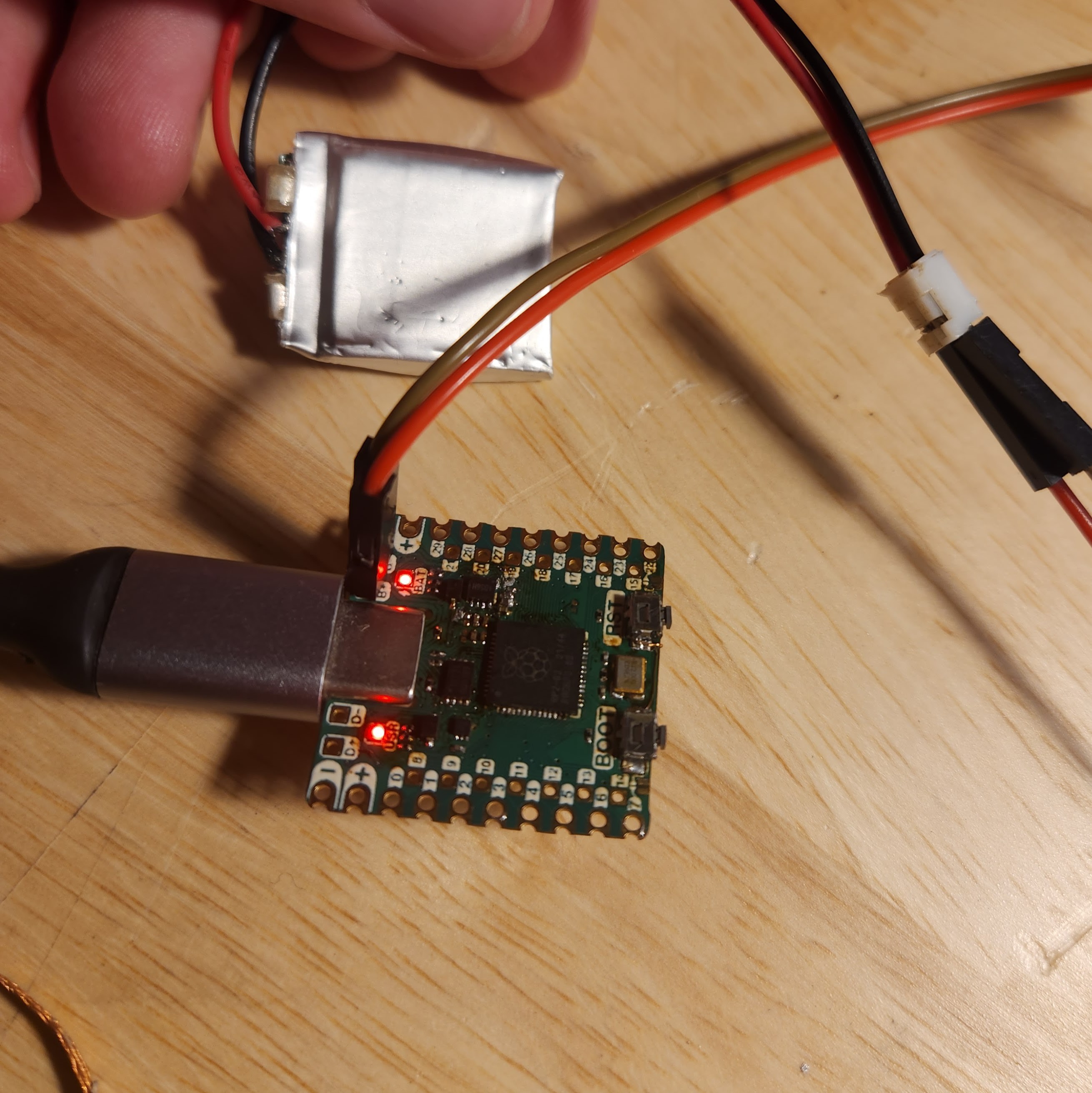
The fun part is that circuit did in fact work. I measured almost 100 mA flowing into the battery when I plugged it in! With the circuit working my next plan was to start messing around with diodes and dummy loads and what not and use this as my test bench.
After sleeping on it (and asking a smarter friend) I realized that would be a dumb idea. The diode really shouldn't have anything to do with it so there must be another issue.![]()
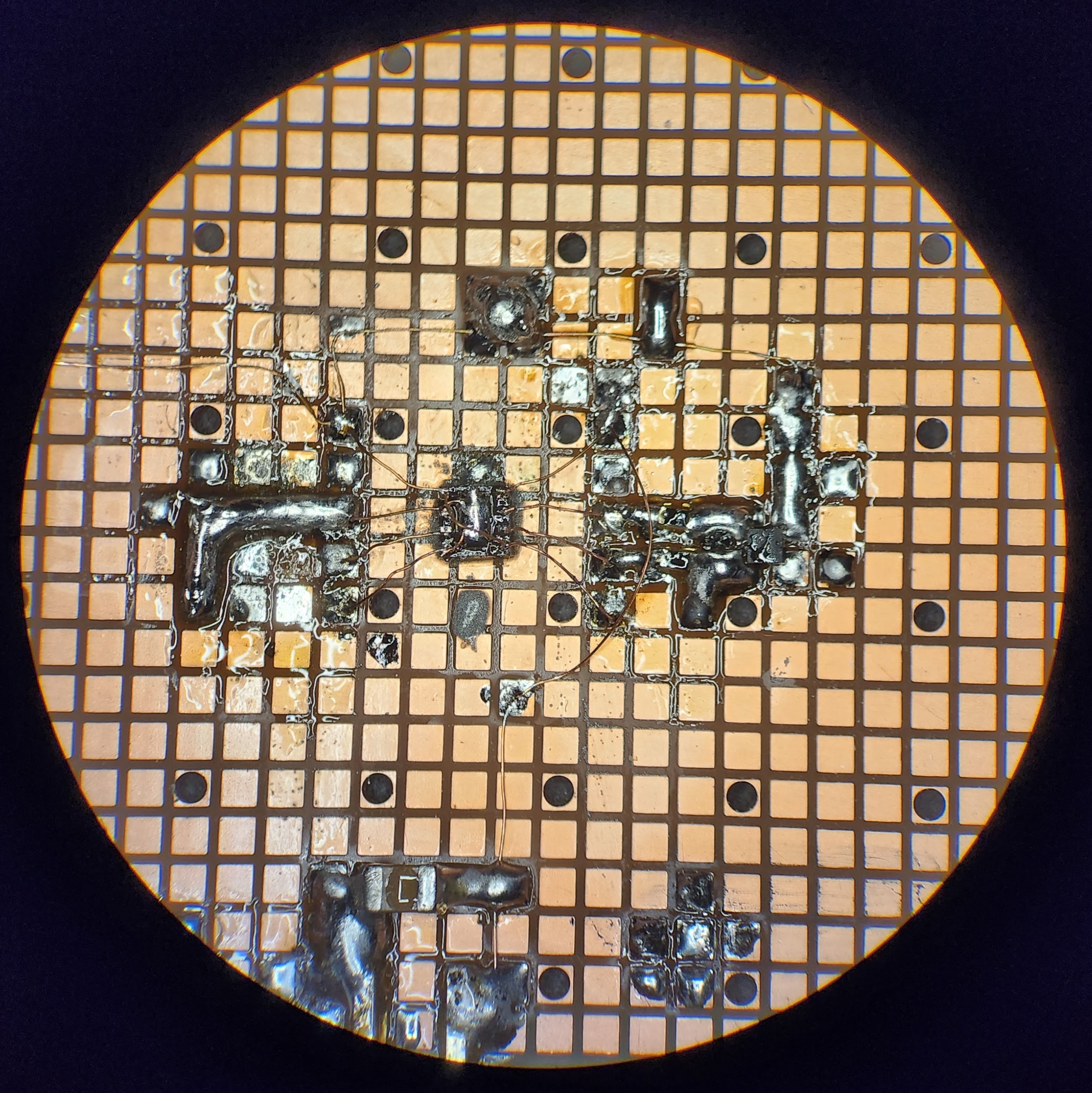
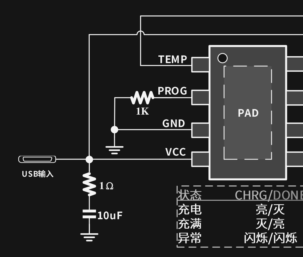
It occurred to me that I didn't actually put a 1 Ohm stabilizing resistor or a 10 uF capacitor on the input. I figured the traces on the board would be high enough resistance to replace the 1 Ohm and that the capacitance already on the 5V bus would be good enough that I could just slap down a 4.7 uF cap and call it a day.
Well after messing around with the capacitors close to the charging IC and observing some interesting and inconsistent behavior I realized that those components were probably included in the datasheet for a reason!So instead of messing around with my crappy dead-bugged circuit I chose to just bodge the proper capacitors and resistor onto my test-board directly.
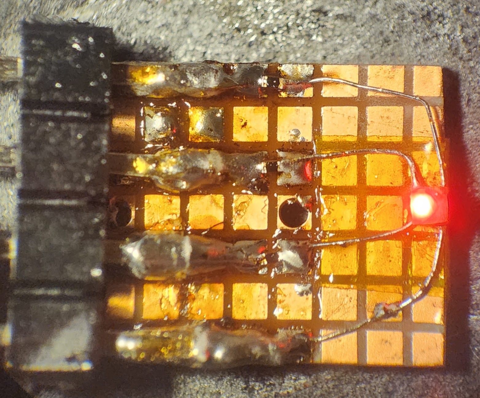
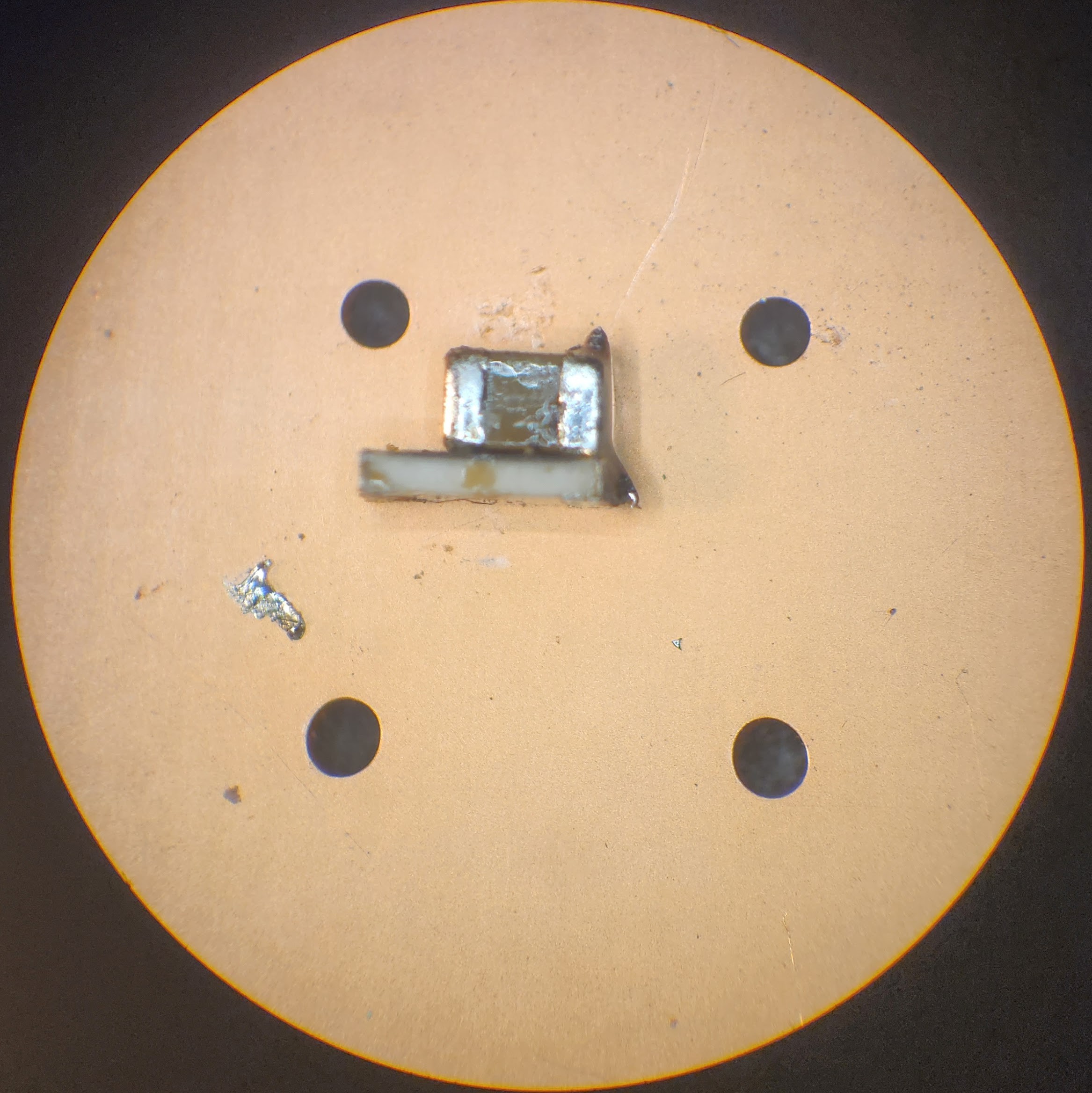
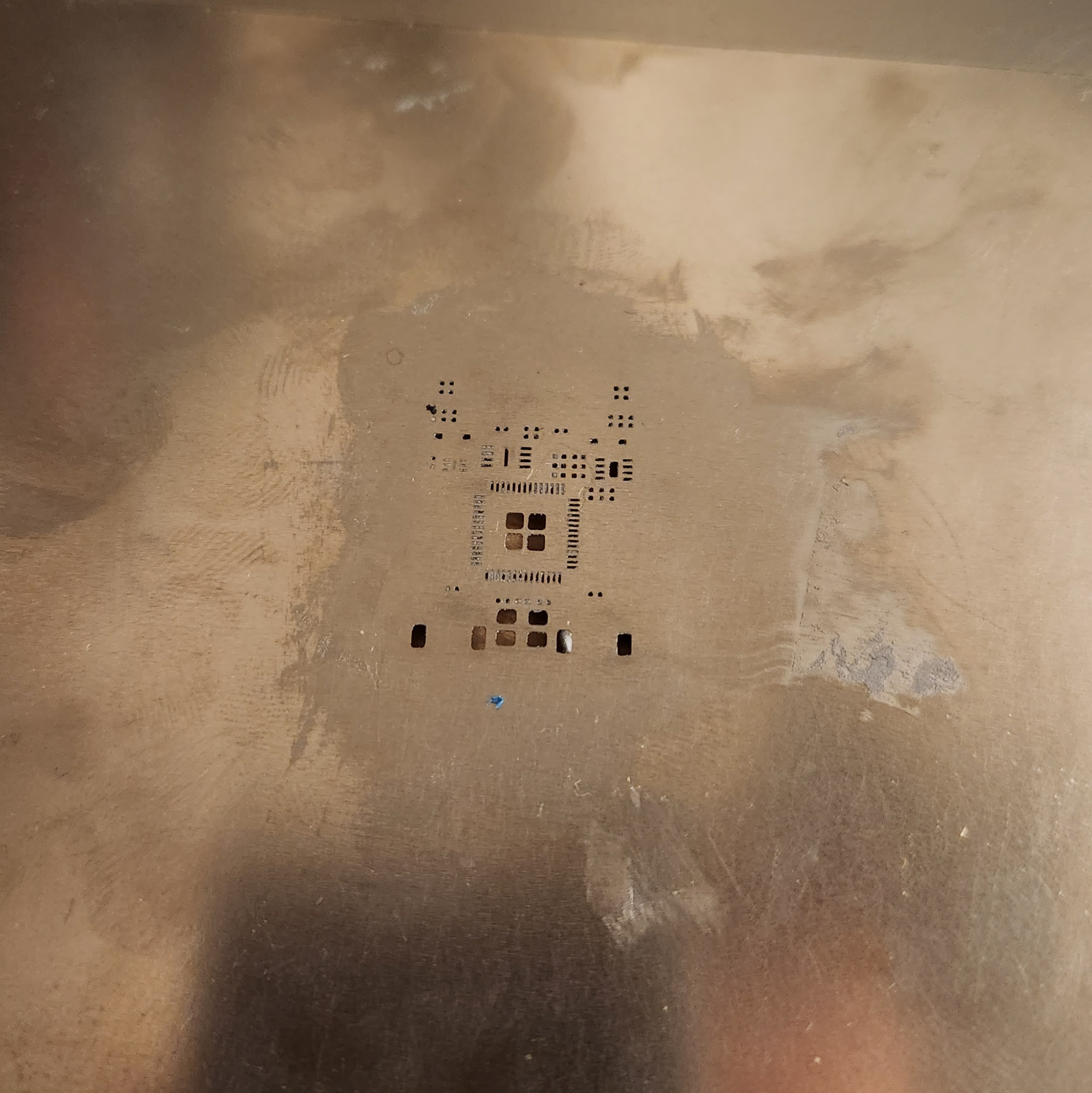
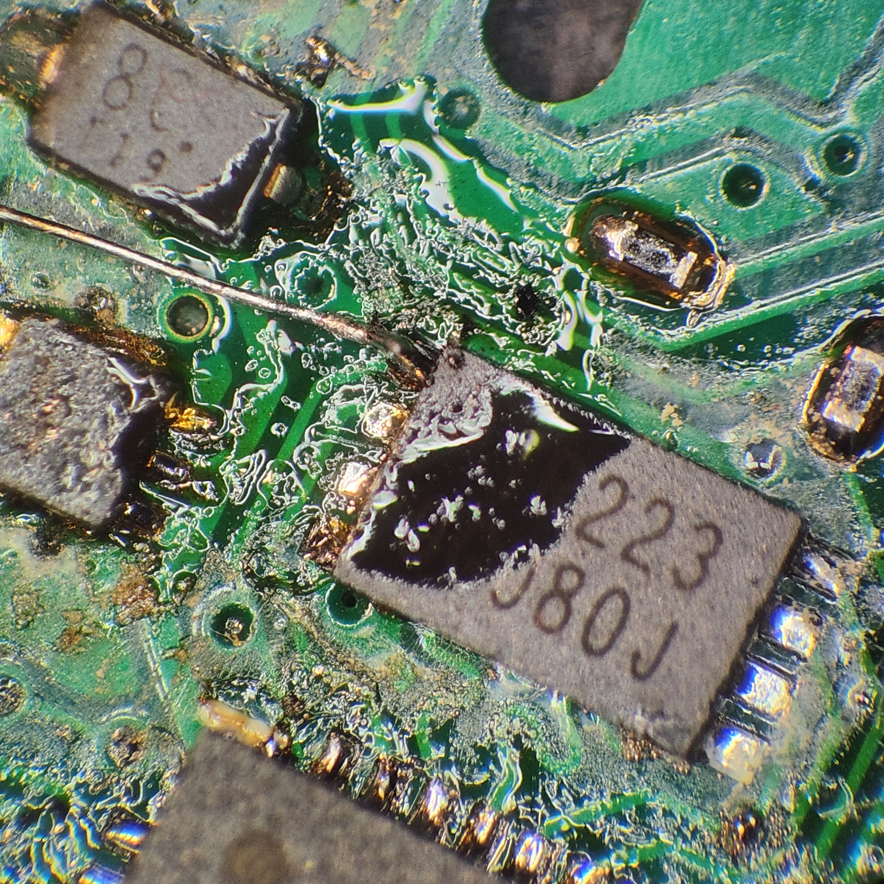
First I stacked a resistor and capacitor on top of each other and soldered their two ends together. The rest was just some time with some very very thin wire and the microscope.
![]()

Remember, datasheets give you example circuits for a reason.
SUCCESS!
This is probably my favorite bodge I have made to the CRAPi board so far just because it's sort of cool to look at. You can see that I added the recommended capacitance to the battery input as well as the recommended capacitance and resistance to the VCC of the charging IC.
Sure enough, after making this addition to the circuit the battery charged up all the way no problem, even with the diode. That leads me to think that there was just some weird instability or oscillation that was happen in the charging IC. This particular IC also has a trickle charge mode that attempts to revive dead batteries with < 1 mA charging currents if it detects an under-volted battery. I suspect that this has something to do with the problem as well, but without the time to stick the problematic circuit on a scope I won't know for sure. Oh well!
Sometimes you just have to move on.Next steps.
This was pretty much the final technical issue with this version of the CRAPi board. I've already updated the Rev. 3 PCB to include more capacitance and the (apparently) very important stabilizing resistor. I am nearly done updating the silkscreen to clearer and more descriptive of the "hidden features" of the CRAPi board.
I've also gotten rid of the (apparently unproblematic) Schottkey diode to handle the power switching. I replaced it with a nice little P-FET. The Schottkey diode was like powering the CRAPi board through a 2 Ohm resistor so it was just burning power. The P-FET has an on-resistance of only 100 milliohms. Is that improvement worth adding another chip to the BOM? I'm not sure! But it does feel better.
After I update the ProtoGrid Rev. 3 will be ready!
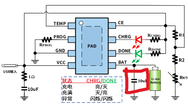
EDIT: Including block diagram and example circuit for for further discussion on charging woes.![]()
![]()
-
Rev. 3 in Progress
09/10/2023 at 05:28 • 0 commentsThis is was going to be a way more in depth post about Rev. 3 updates but then my laptop died and nothing saved so I guess I will just type up a quick version for now.
There are a few main things that I need to change in Rev. 3. The biggest issue so far is that the battery charge never charges the battery fully. It only gets to 3.9 V. After some thinking and some tinkering I figured out the problem, and this was a great learning moment!Battery Charging Woes
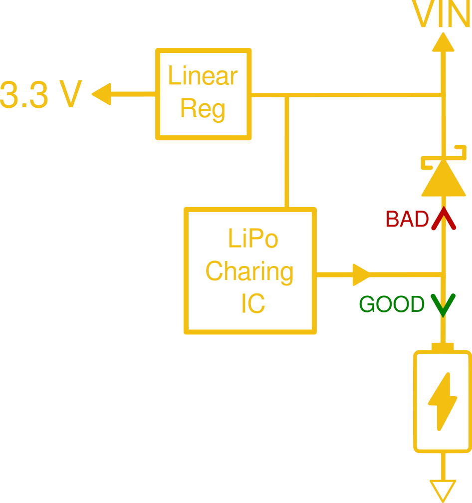
To handle the power switching between USB and battery, I threw a diode in front of the battery. That way VIN wouldn't go to the battery directly but when USB wasn't connected it would be the battery powering the system via the linear regulator. The problem?
What happens when the battery is no longer the path of least resistance.
![]()
That's right, at a certain point in the charging the diode became the preferential current path meaning the battery never increased fully charged. After looking at the data sheet for the diode it worked out to a forward drop equivalent to about 2 Ohms. The fact that the impedance of the battery was high than 2 Ohms seemed strange to me but thinking about the crappy contacts and connectors it made sense.
I was able to confirm this theory but removing the diode and letting the battery charge up. Sure enough, that worked! I got the green light!

The battery charging solution
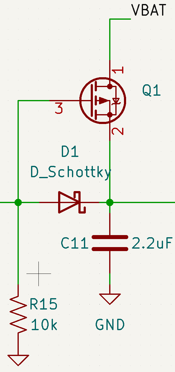
I poked around a little bit and realized that I just need to stop being lazy. The more correct way to handle this power off is with a P-FET and resistor.
![]()
The idea here is that the P-FET acts like a Normally Closed switch. It will happily conduct until you hook up a VIN that pulls the gate higher than the source (P-FET are weird) and the P-FET opens, protecting the battery. I think this is something called an "ideal diode" configuration, or something like that.
Anyway! Figuring this out was honestly the easy part. The hard part was
1. Integrating ANOTHER chip and resistor onto this board.
2. Finding a small, cheap, and least crappy P-FET I could find.
In this case the "crappiness" is defined as the On Resistance of the FET. This parameter was especially important to me because when running on battery power you are running all the current through the FET. So if there is a super high on resistance that is basically just burning power.
Assuming an average current draw of 10 mA (just to make the math easy), using a diode in the configuration above gives a drop of about 2 Ohms. I managed to find a P-FET for cheaper than the diode with an on resistance of just 100 milliohms! Now we are talking!
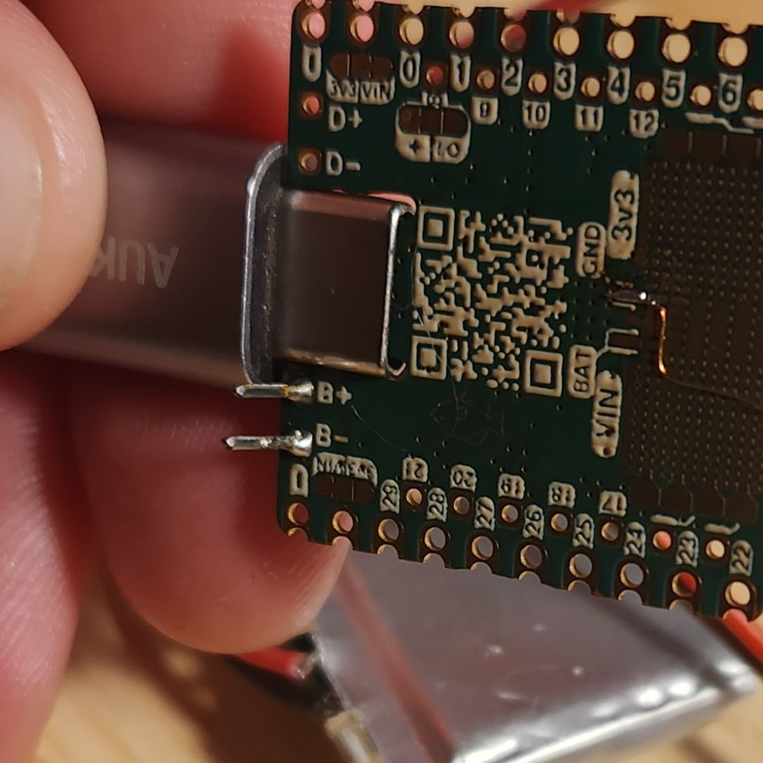
The next hardest part was just integrating it into the board! Thankfully I managed to do it without too much frustration. You can see the P-FET and extra resistor on the right hand side of the image below. This thing is TINY. Just 1.3mm by 1mm! What a time to be alive!![]()
That's all for now. Slowly I am moving towards Rev. 3! Like I've mentioned before, I will be trying PCBWay for the next round of boards and I am super excited to get some more microscope pictures!
-
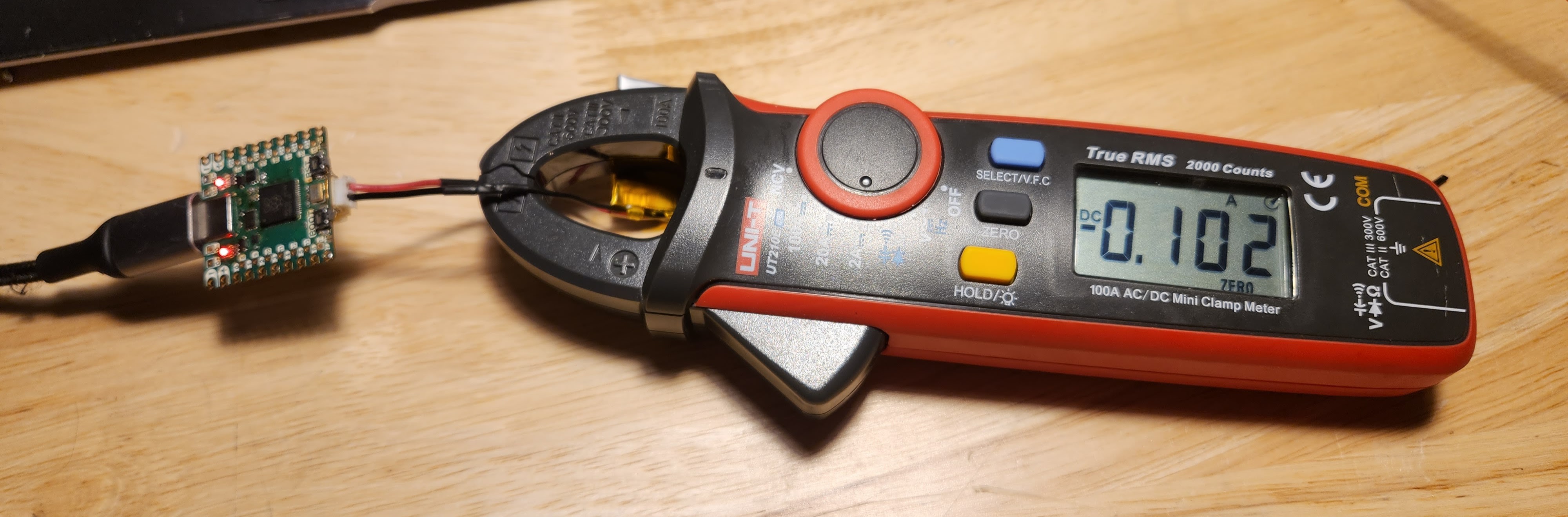
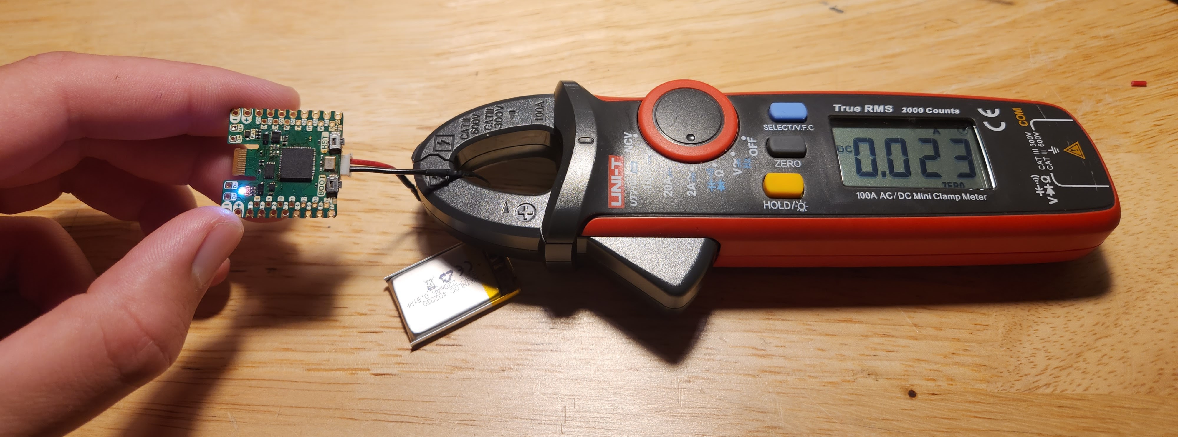
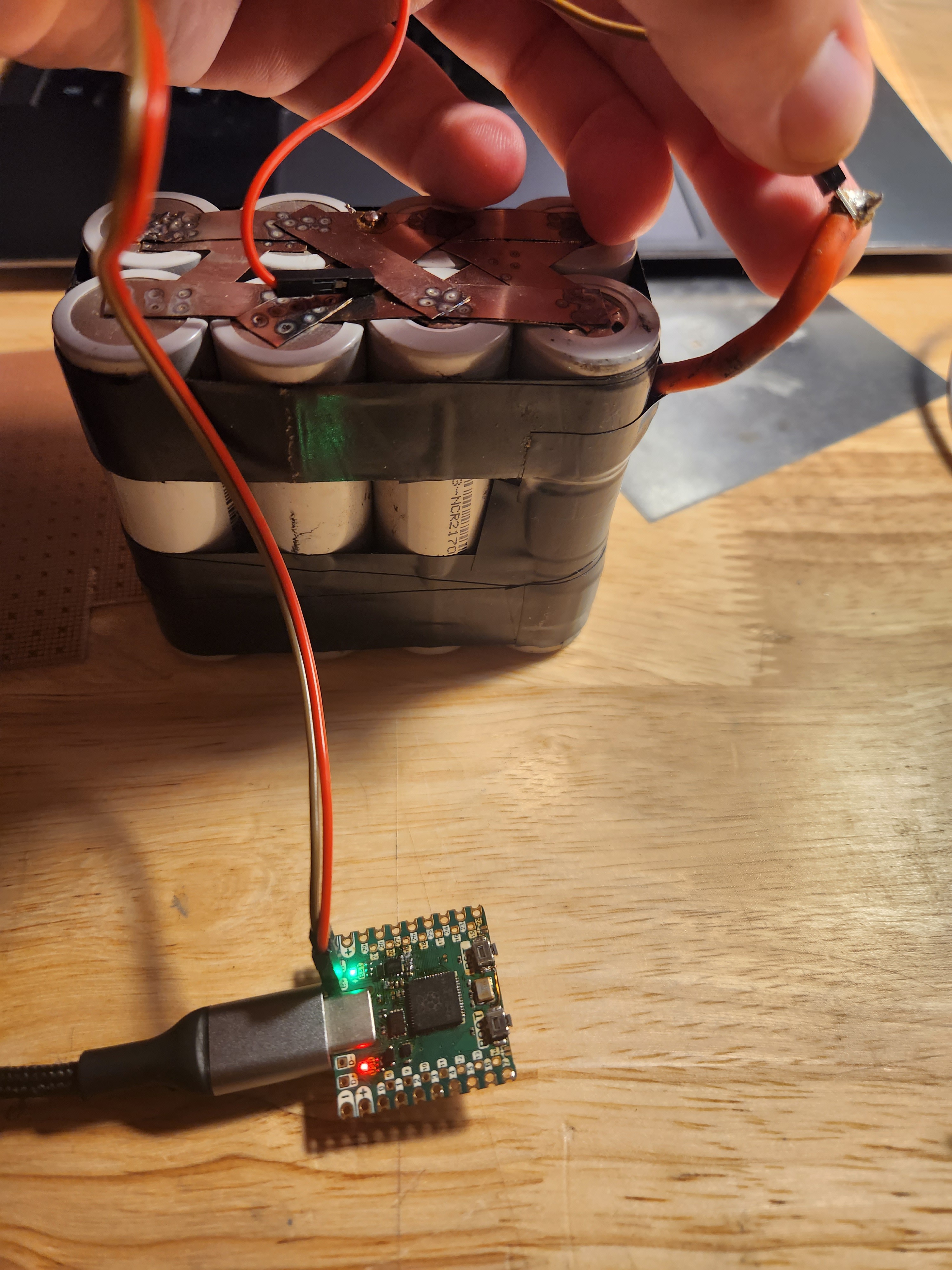
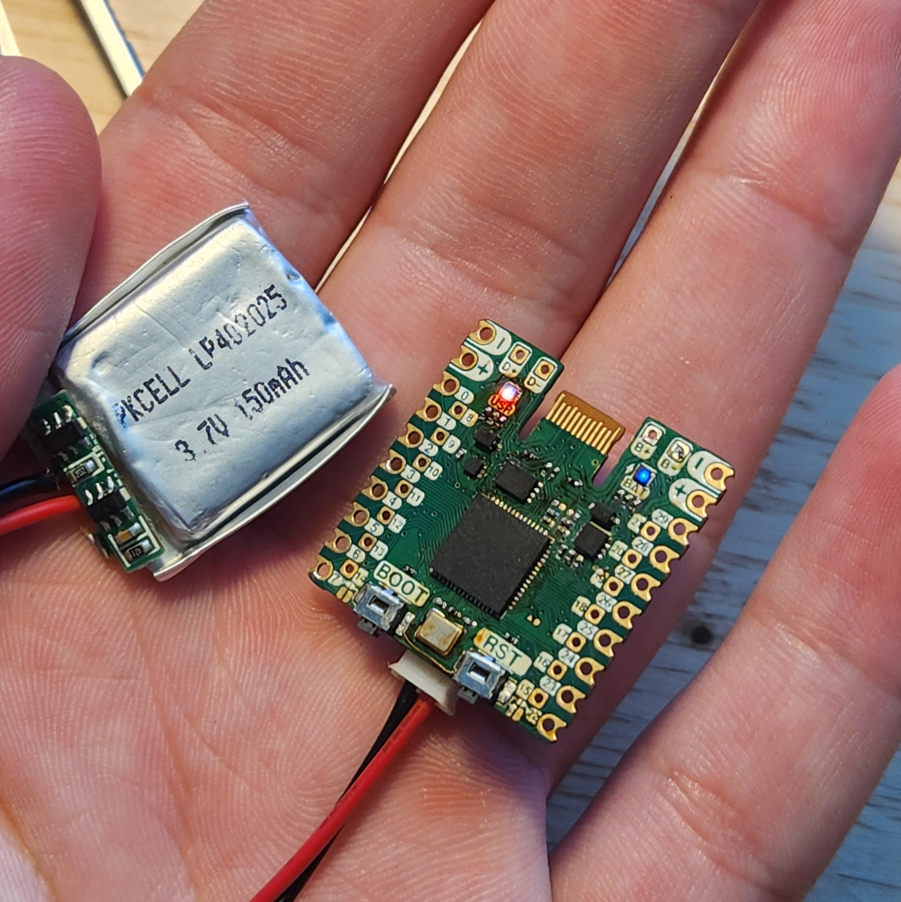
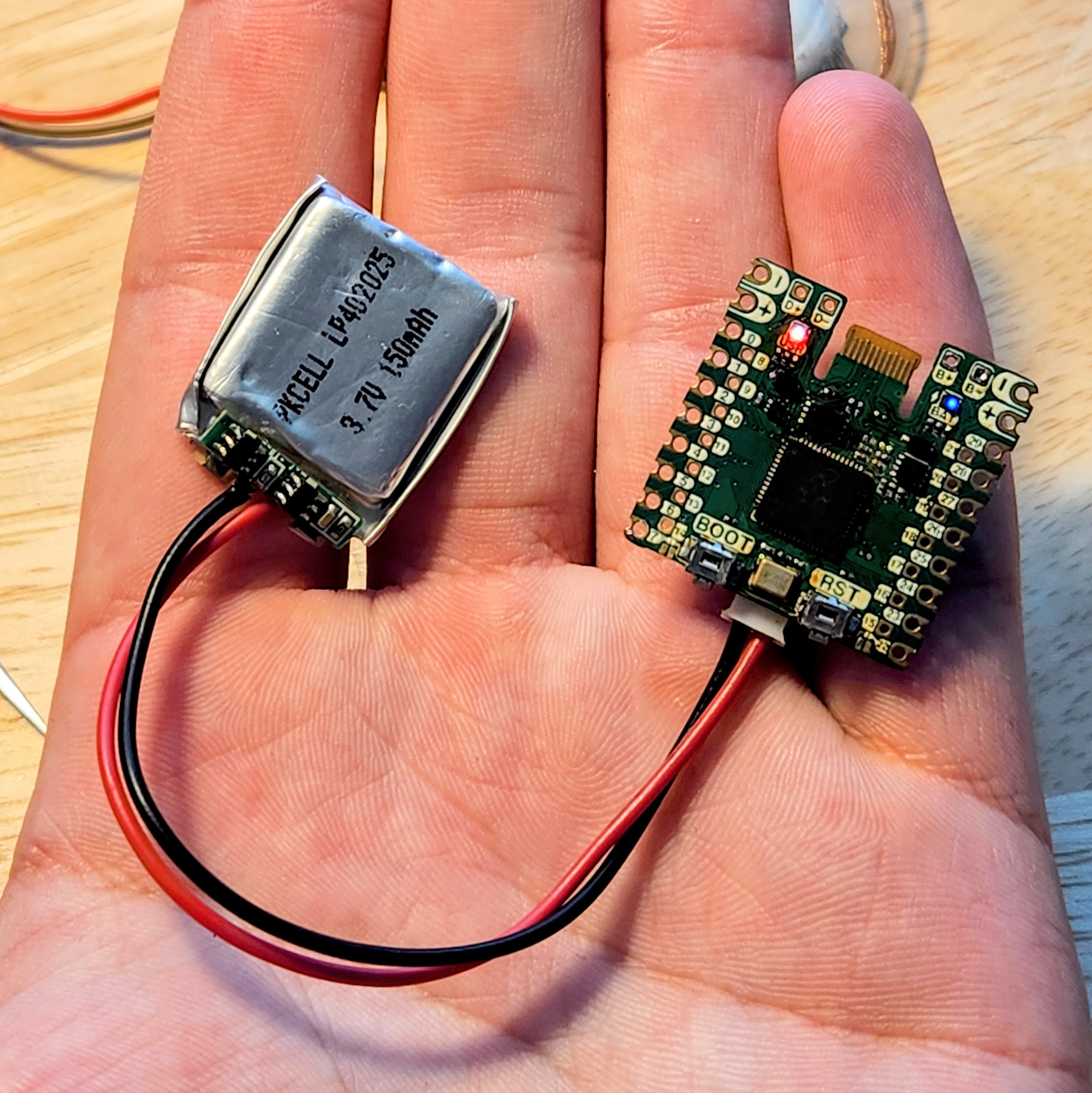
Rev. 2 - LiPo Current Testing and Questions
08/16/2023 at 16:20 • 0 commentsJust a quick log today. The last log had me checking my biggest "creeped" feature, as it were: the LiPo Charger.
I bought a less sketchy LiPo cell and borrowed a suitably accurate clamp meter from a friend.
![]()
Don't let labeling on the meter fool you! The firmware on the meter had been reconfigured to measure 6000 counts rather than 2000. Considering that the charging IC was configured for 100 mA charge rate I would call this a win!
This setup is also convenient for power draw measuring too. Sitting idle with an install of CircuitPython and with the R, G and B LEDs turned on, current draw measured anywhere from ~25 mA to ~35 mA, which seems to be in the ball park for the RP2040. Eventually I would like some more power logging / bench marking.
![]()
I also wanted to look into an issue that I mentioned in my last log.
For some reason, if you unplug the USB cable while charging the battery, and then try to immediately plug it back in, the charger does not respond: no indicator light and no current flow. If I wait for a while, running off battery power (so no power cycle) and try plugging in the USB again, then it will charge as normal.
I know that these chargers can normally have some sort of hysteresis but 1+ minute seems a little strange. I am wondering if the Schottky is messing with the LiPo charger some how... maybe I should investigate a more graceful switching option for Rev. 3 of the board.
If anyone has any ideas for this issue I would love to hear your input!
-
LiPo Charging - First Try!
08/14/2023 at 03:13 • 0 commentsThe last log on Rev. 2 got a bit into the weeds. That's my bad. Another product of my late night brain but hopefully you got the gist... These posts always take way longer than I think to write because I keep thinking of things I want to include!
Anyway, hopefully this log will be less rambly because today I tested out the last core feature of the CRAPi2040 board: LiPo Charging.Spoiler: I nailed it first try :D
Nothing ever works first try so this is sort of a big deal for me.
![]()
Here's an up close, but crusty, shot of the LiPo circuity. Sorry about that.I was pretty deliberate in the choice in my charging IC. I had two primary criteria:
- Small as possible
- Constant Current and Constant Voltage Charging.
This random chip that I picked from LCSC does both of those things... Well, I am 100% it does the "being small" part well. Only about 80% sure on the CC feature as the entire sheet was in Chinese and the PDF translation on Google refused to work for some reason. I got around that by using that cool live camera translation thing on my phone.
As a side note, this was my first experience with LCSC and it definitely has it's uses. If you can fill in the blanks in some of the translations you can find some really niche stuff. The main reason I went to LCSC is because Digikey didn't have any appropriately minuscule LiPo charging ICs. The shipping was reasonable too considering it's an ocean away. If you are looking for something very particular and haven't already, checkout LCSC!
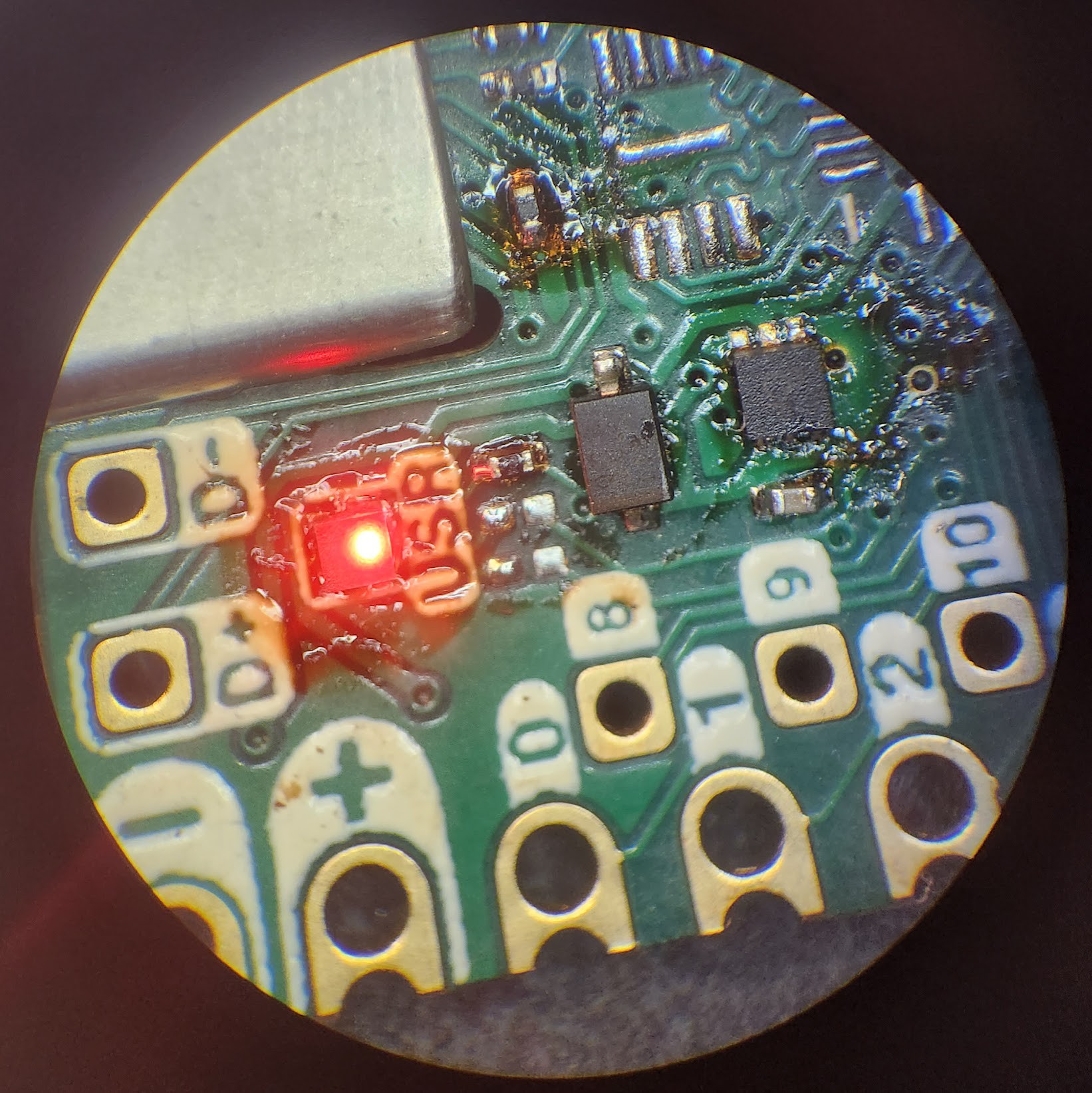
Here's the picture of success that made my day!
![]()
Look at those two beautiful RED LEDS!
The first red LED is the power but the second red LED is the charging indicator!! The bad boy popped right on the second I hooked up that beat up LiPo. Also, if it wasn't clear. That second LED (labeled as BAT), is RGB. The R and the G is hooked as the status LED for charing and the B is hooked up to pin 25 so that code meant to run on the Raspberry Pi Pico will port over well.
I wasn't patient enough to let scary LiPo try to charge all the way, so I jammed some jumpers onto some batteries that were already fully charged to see if I could get that green LED to show it's face.![]()
And there it is! YES. AMAZING. That feels so good. And by the way, this is only a 1 cell charger. The connection above is just testing one set of batteries in a 2S4P string.
![]()
Green Green Green Baby!
This also shows off one of the changes that I made to the Thads in Rev. 2 that I don't think I have mentioned yet. On Rev. 1 of the CRAPi board I had these really really tiny plated through holes which probably were sort of useless for getting solder to flow through.
![]()
![]()
In the second revision of the board. I made the holes way bigger. This is for two reasons:
- It will probably help when soldering the Thads to other boards
- AND they are the perfect size for those bread board jumpers that everyone uses.
The picture below sort of shows what I am talking about from the bottom view. The holes are just just tight enough to use as a friction fit but that's probably a bad idea. Also note the 0.1 inch spacing!
![]()
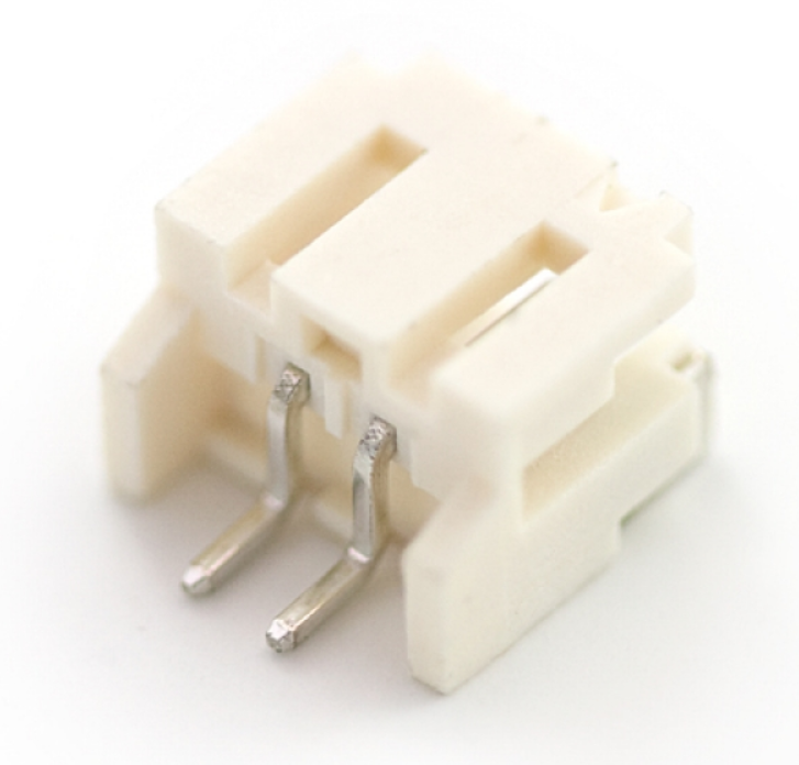
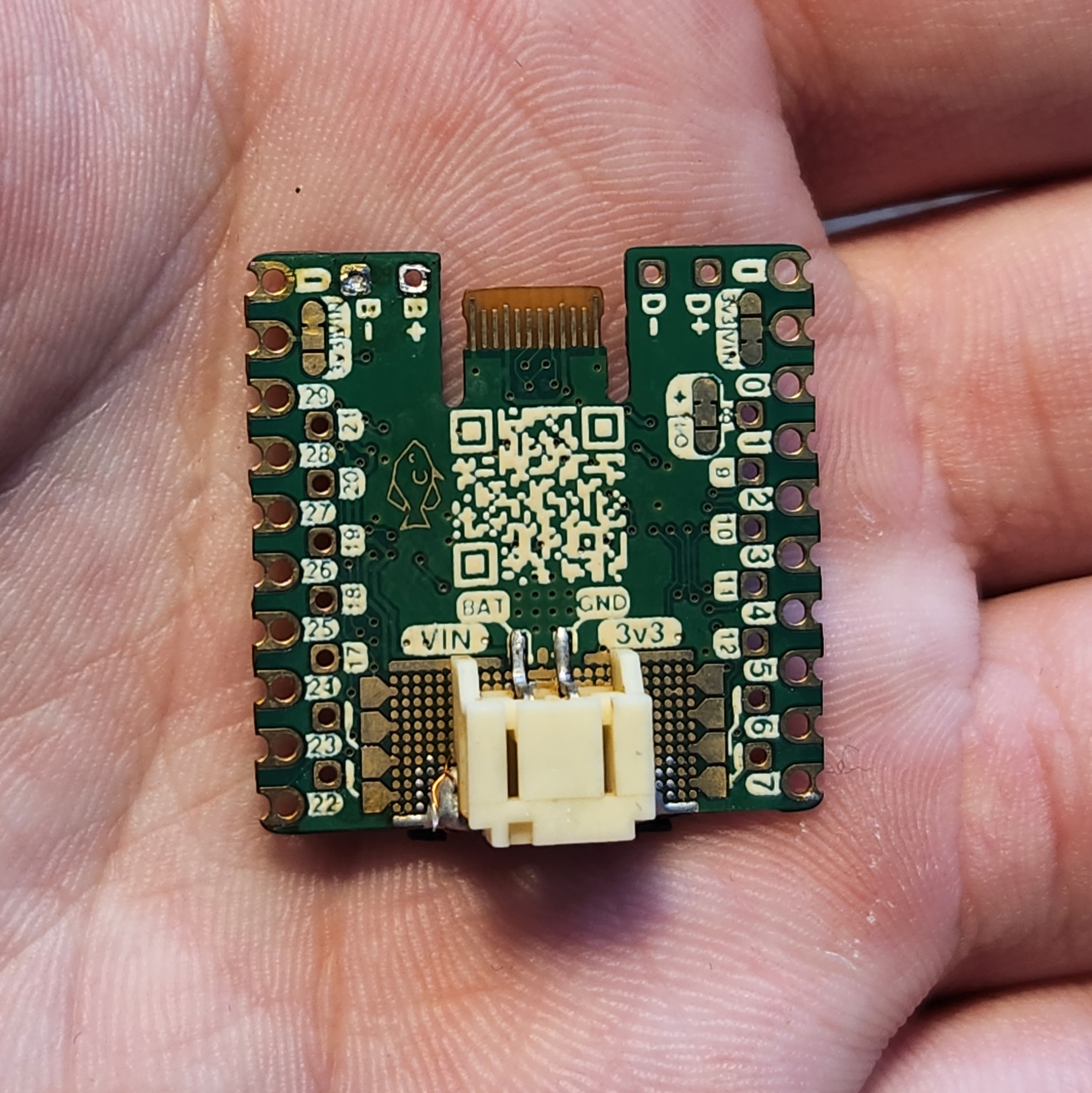
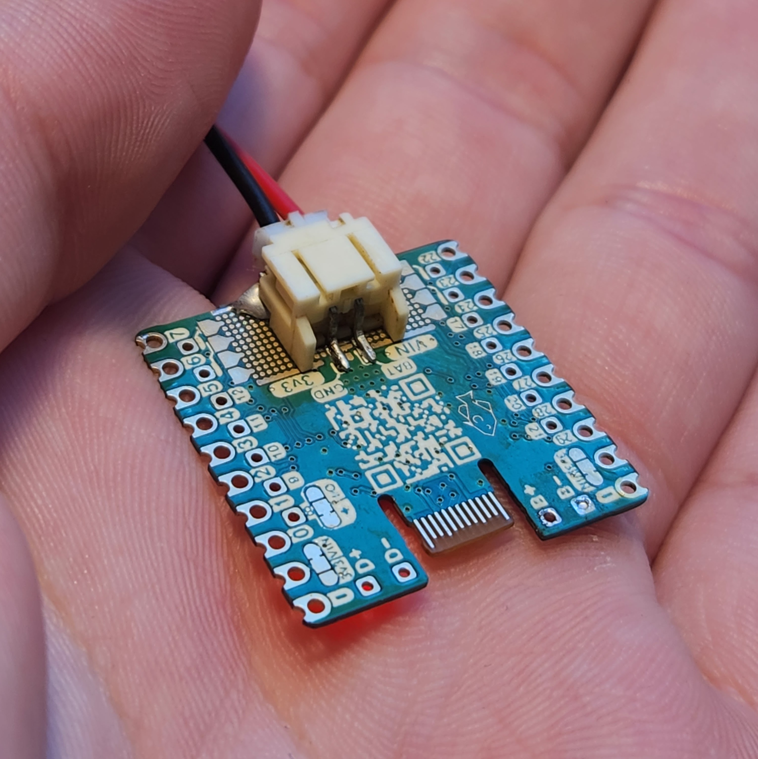
In all of this excitement I almost forgot to test another feature that I labored over in Rev. 2 on the ProtoGrid. I succeeded in jamming a (somewhat hidden) right angle JST connector footprint onto the CRAPi board! You know, this one:
![]()
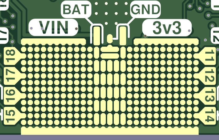
Direct your attention to the BAT and GND labels. Those aren't just for show! Those skinny little pads are basically the exact same width as the leads of the JST-PH connector shown above. Obviously, I didn't have much room to work with so I wasn't sure if this would even work.
Again, to my surprise: the footprint worked perfectly. The front anchor tabs of the connector have no problem being soldered down to the GND rail at the bottom of the ProtoGrid. I'm pretty sure I was designing this on a train to Chicago in the middle of the night. So, I don't really remember designing this, but I am glad it worked out!
![]()
![]()
![]()
![]()
![]()
![]()
Sorry for all the picture spam but I am just so thrilled. It just looks so CLEAN. I love it. The connector takes up the entire ProtoGrid, but hey, that's why I broke out the battery connections to more than one place. The CRAPi board is about flexibility, remember?
![]()
I am also happy to report that the power source switching seems to be working. Starting off on battery power and plugging in USB power the red charging LED illuminates. It shuts off when I remove the USB as well. Repeating this cycle more than once seems to yield inconsistent results so more investigation is required.
At least it works once though! I had never thought about the circuity needed for power supply switching on LiPo enabled dev boards. I took the easy route out and just slapped a Schottky on the battery terminal (cheap, remember)? Because of the diode drop it means a less than optimal voltage range from the battery. However, it does mean one less item on the BOM because I am using the same type of diode for reverse polarity protection on the VIN line.
If the Schottky ends up being a problem then maybe I will consider finding a tiny P-FET to handle the power supply hand off a bit more elegantly.
What's next?
Either way, I think that wraps it up for this log! At this point I have tested everything that I needed to on Rev. 2 of the CRAPi board!! I am so excited to have this project asymptotically approaching "complete" so that I can start using it in my other projects.
I am thinking about some base boards and adapters that could be useful for the CRAPi board as well. I am a big fan of the "use only what you need when you need it" mentality, and the idea of adding on beefier functionality to the CRAPi board in the form of a baseboard or add ones would be cool. I am thinking maybe a little back pack that includes mounting holes, or an on board regulator with a crazy wide input range.
I'll also be giving PCBWay a try for Rev. 3 to see what their quality looks like. Armed with my microscope I am super pumped to do a comparison and see how they handle some of my wacky ideas.
What do you think?
That being said, I have a mental list of bug fixes to make in the next revision of the board. However, it has occurred to me that more than one person might want to use one of these things (thanks, James!) so I am wondering: what cool ideas do you have to make the CRAPi board even better?Let me know!
-
Rev. 2 Assembly and Blinking!
08/11/2023 at 03:39 • 0 commentsPreviously, we took a look at some gorgeous ENIG plating, clever silk screening, and a USB-C connector that consisted only of the 0.6mm PCB substrate that the rest of CRAPi board lives on. Honestly, I almost didn't even want to put the boards together. Seeing them come out so well made my week! The thing is, this isn't my first rodeo, I know how these things go.
Here I am feeling like a smarty pants with some shiny boards and cute little components, but I already know that this isn't going to work on the first try... but we must push on! The only way to turn the unknown unknowns into known unknowns, and eventually into known knowns is to just slap a board together and pretend that everything will work on the first try.
Now if I was smart, I would assemble the board bit by bit, ensuring that each component is soldered down and working as intended. If I was this hypothetically smart engineer, I would test my board by assembling things in the following order:- Linear Regulator
Rule No. 0 of Electrical Engineering: Make sure it's plugged in. - Processor
Once the heart is beating, gotta make sure the brain is thinking - Flash
Once the brain is thinking gotta make sure the brain is remembering - Everything Else
Everything else is really just a bonus to me...
So with this plan in mind. I am going to completely ignore it and just put the board together all at once and hope for the best! Sometimes being smart and optimistic is mutually exclusive, and there's nothing you can do to stop me!
Assembly!
I mentioned it in the last post, but one of the changes between Rev. 1 and Rev. 2 was the move from 0402 components to 0201 components. In my head I knew that 0201 components were half the size of what I had gotten used to on Rev 1, but its a totally different thing to actually see how tiny these things are.
![]()
I mean look at this! Look how dumb and tiny they are! That's the tip of a pen! Man that was intimidating. I tried my best to only remove the number of components that I needed from the tape, but of course a few extras popped out now and again. It literally felt like brushing sand off my desk, if I felt it at all. At least clean up is easy. Just need to vacuum it up with the rest of the dust on my floor!
Once I got over the grains of sand that I would be trying to work with, it actually wasn't too hard. I had a pretty nice pair of tweezers and my eye sight is decent so populating and positioning those itty bitty Rs and Cs wasn't much harder than with 0402 components.Armed with my solder stencil and paste, I lined everything up the best I could and gave it a good swipe to make sure that I got all the pads covered.
![]()
I carefully placed all the components into their respective locations yadda yadda, threw that thing on my crappy hot plate and watched the magic happen
Assembly Problem #1 - Solder Paste Trouble.
I mentioned that my cheap little hot plate gave me some problems in the last post and that I managed to mitigate them by heating up the hot plate with the PCB already placed on top. I did not have such luck with this new problem.
![]()
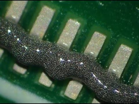
In case you have never seen it up close before, heres a random picture from the internet. Ypi can see that solder paste is just tiny balls of solder in a suspension of flux. Of course, the flux is supposed to melt first, and in the process clean the metal joint of oxidation that would prevent the solder from properly wicking on to the joint and mating the two surfaces
The interesting problem that I was experiencing is that the flux bubbling and boiling under my components created enough force to knock around the 0201 components. Because the flux melts before the solder does, there is nothing to hold those little grains of sand in place while the flux does its thing.
Eventually I'll look into the problem; obviously this has been solved.For now though, I don't really care!. Instead of mucking around with different types of solder paste or throwing down a few Alexander Hamiltons on a better hot plate I came up with a different method.
My SMD method in the form of an ordered list:
- Tin all the pads with my soldering iron. Tinning the tip of the iron and rubbing it on fluxed-up pads was good enough.
- Add more flux on top of the pinned pads - this is what will stick down the components
- Add your components to the pads (duh.)
- Throw the board onto the plate and and prepared to be satisfied.
There is something to be said about not over thinking....
You would think that this method would lead to the same flux bubbling issue, but it didn't. I guess the flux that comes out of my pen isn't as prone to the bubbling? Either way, it proves that you can do SMD reflow without making a mess with stencils and paste.
Assembly Problem #2 - Bendy Boards
Alright great, all the components stuck down soldered up, good to go. But then I noticed something: my boards were bending! After my first round of reflow I was looking at my pads under the microscope and noticed that a few of them weren't connected all that well.
I threw the board back on the hot plate to be reflowed and noticed the edges of the PCB starting to curl up! I am not sure if this was the sole reason for some of the missing connections. I am sure, however, that the crappy hotplate combined with the super thin PCBs didn't help. If I ever make these in quantity maybe I will splurge on something with reflow profiles. Better yet, I could use a CRAPi2040 board to modify a toaster oven and just make my own reflow oven!![]()
Here's an example of some poor connections on the solder pads. They aren't completely disconnected but they aren't great either. My (somewhat ironic) method of cleaning up these joins is just smearing a thin layer of solder paste on the side of the chip and hitting it with my soldering iron.
![]()
Still crusty, but better! I had to do this same process w/ the flash chip as well. Side note, does anyone know how to make things less crusty? I have seen some "no-clean" flux laying around at work and it seems to work as advertised. Having a microscope is a blessing and a curse...
TIME TO BLINK
Assembly was surprisingly smooth other than those two little snags. Once I got into a rhythm and warmed up a little bit, placing the components wasn't any worse than the 0402s from Rev. 1. It's funny how you pick up on little manipulation tricks when things are this tiny. I quickly honed the skills of kick-flipping components by gently pushing down on their edge. I also realize the importance of clean tweezers!!! Even just the tiniest bit of flux residue left on the tip of my tweezers was enough to prevent the components from releasing when they were dropped.
So after an intense learning period of about 45 minutes (roughly the time it took to put the very first board together) here is what I was left with!!!![]()
So pretty! (sorry for the shaky picture) Now time for the real question: DOES IT WORK???
Answer: NO!
When I plugged the USB-C connector in I didn't get any signs of life. The red power LED stayed disappointingly dark and there wasn't a peep from the RP2040 when I plugged it into the computer. Am I surprised? Nope! Disappointed? Maybe a little bit... Here is where things get interesting i.e. Why aren't things working?
The Troubleshooting Trifecta - ∆
Retelling this debugging process in chronological order would be sort of difficult because it took a few days and happened in a non-linear fashion. In retrospect, I may have addressed and solved problems that weren't the current cause of the non-functioning board but were still problems. The truth is I don't remember which problems were solved first. I've only got two brain cells, remember?
The problems:
- Matters of perspective.
- No ground for you!
- Missing capacitance on the linear regulator!
Problem #1- Matters of perspective.
So the LED isn't lighting. Weird! Well first thing to check is if we are shorted to ground. A quick check with the multi-meter says otherwise! We are getting 3.3V out when plugged into a 5V USB supply. Nice! ...and surprising?? These linear regulators are TINY and I was almost certain that I had shorted something under the IC. Try to guess which chip it is in the picture above, I dare you! I was also certain that the LED wasn't either, so what gives?
Well: I got my silkscreen wrong!
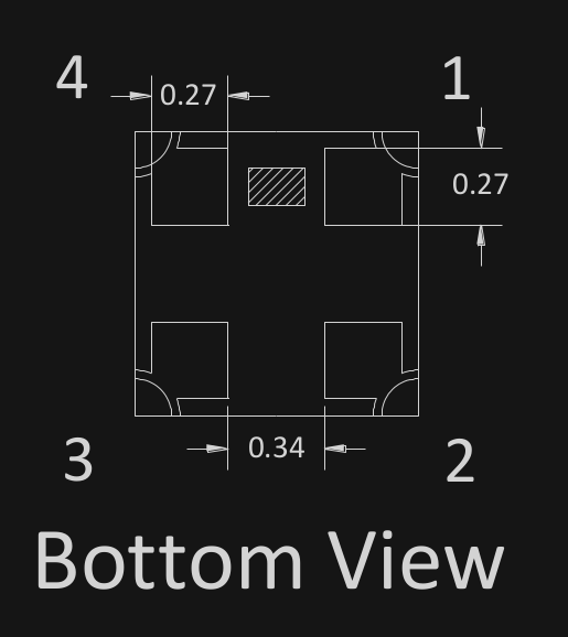
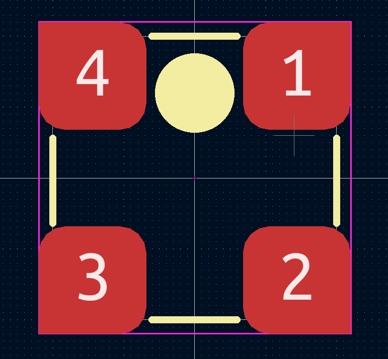
I am using a common anode RGB LED, that indicates polarity with a tiny little dot on the bottom. The data sheet gives the following diagram. Easy right? A bottom view of the chip and some dimensions, a few minutes later and I have my footprint in KiCAD
Here's that bottom view I was talking about.![]()
And boom, heres the foot print. I even took some liberties with the pad design to hopefully discourage shorted pads. Notice any problems?
![]()
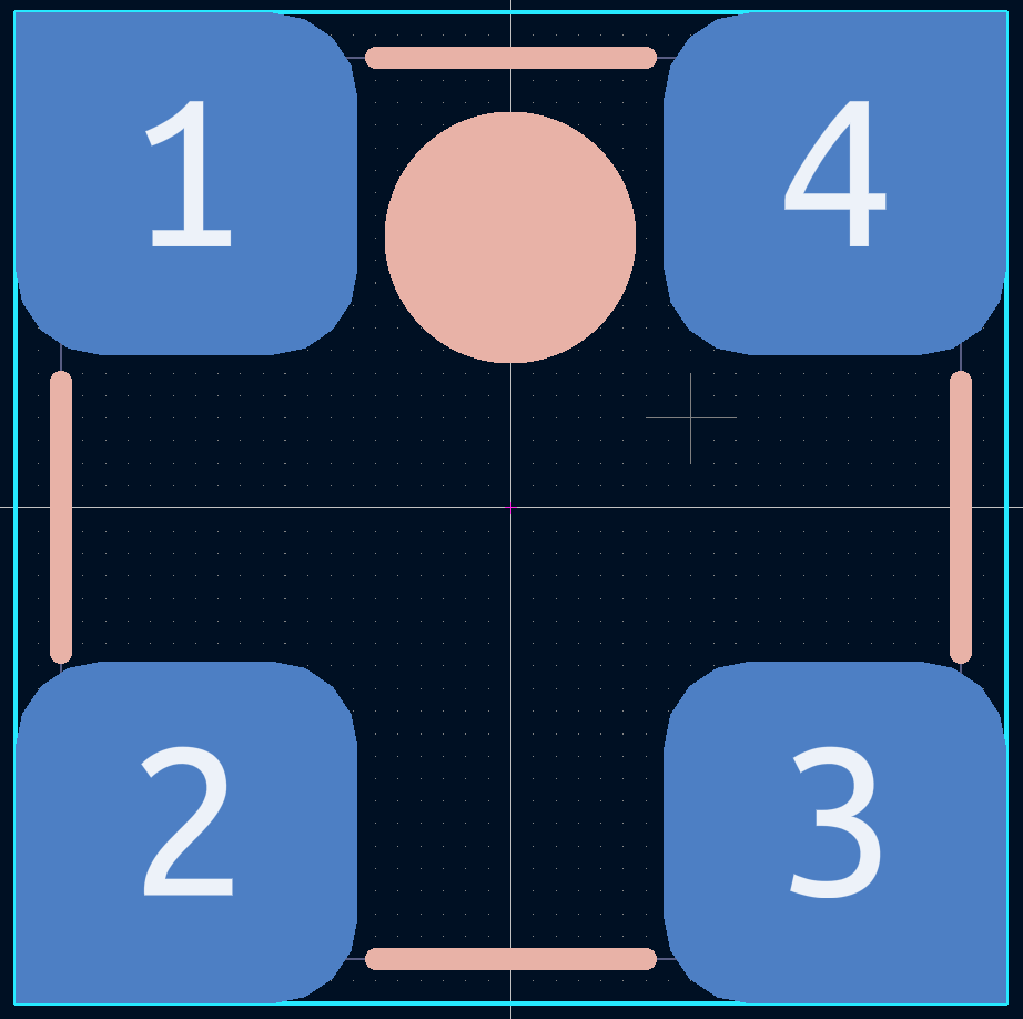
Well I'll give you a hint. The datasheet provides a BOTTOM view and you typically design a footprint from a TOP view. In other words, I'm always used to looking down onto a footprint when I am making on in KiCAD. The footprint SHOULD have looked like the one below. Notice how the pin numbering is mirrored.
(just imagine that the pads are red, okay?)
![]()
Solution: Just rotate the LED 90 degrees (and double check foot prints)
This was one of those sneaky little problems and I am pretty proud of myself for staying focused and working out the issue through process of elimination. The way things worked out, a rotation of 90 degrees is all that is needed to get the red LED doing it's thingSo pretty! Great job LED!
![]()
Problem #2 - No ground for you!You know the LED problem wasn't that bad, I thought about things logically, tested my theories and finally converged on a solution. Things get a little fuzzy from here.
My problem was eventually this: the RP2040 would always go into boot mode regardless of the BOOT button state on powerup. The RP2040 would always present itself as a storage device to the computer.
I thought I had seen this problem before, it was like the RP2040 didn't have any flash attached to it. I had the same symptoms on Rev 1, so I thought this would be an easy fix! The strange thing is that I had fixed that problem with Rev 2. Darn! That meant I would have to think and stuff...
I was still suspicious of the flash from my Rev 1. so I focused a lot of my inital efforts there. On the Rapsberry Pi Pico schematic there is a DNP pull-up on the CS pin of the flash. I am not using the same exact flash chip so adding a pull-up on the CS line might be a good move.![]()
![]()
The good news is that I got to use my ProtoGrid (needs more tweaking I think). The bad news is that this didn't do anything... The chip would still present itself as if there was no flash. This would happen even after trying to upload something to it. It would just eat the file, disappear and then reappear in my list of drives.
Solution: Check your footprints, make sure everything is grounded, try it anyway.
So a few different issues. The first thing I noticed that part of my ground plane wasn't connected. I had been poking around in continty mode and noticed that my buttons and my clock were on their own little island.![]()
Ugh. Yup, there's a ratsnest. I do most of this work late at night so I must have missed it in the DRC.
After finding this problem my therory was that the clock wasn't actaully working but the RP2040 uses the interal ring osccilator for USB functionality so it was still showing up as a mass storage device. I dunno. Either way that was an issue, and I bodged both the buttons and the crystal to ground.
That lead to the same behavior of just perpetually remounting after being given a perfectly good firmware file. which led me investigate the buttons directly.
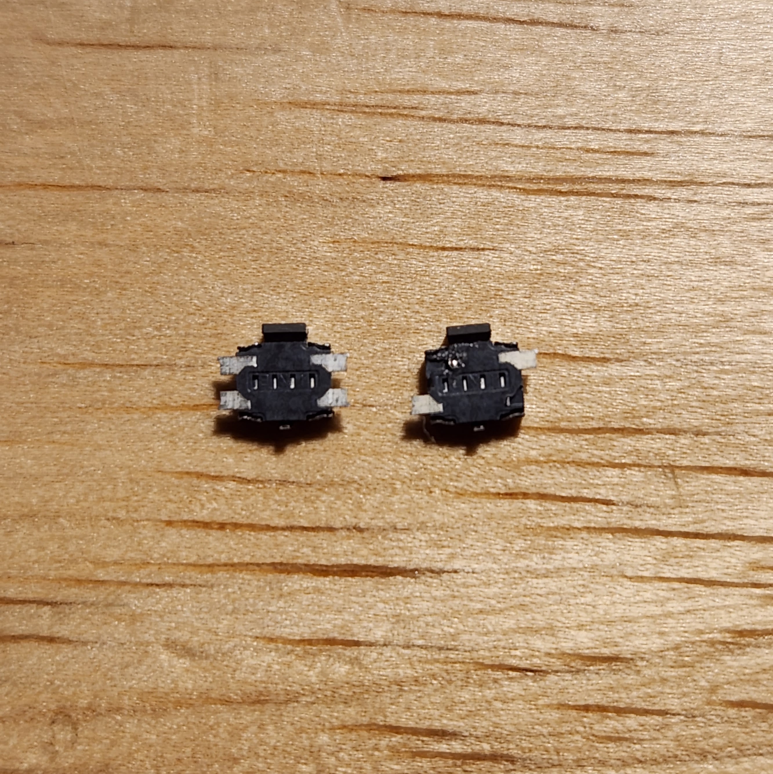
In the few months it took me to order them, the right angle tact buttons I had picked out went out of stock. I didn't feel like making a new footprint so I found other buttons that would fit on the old landing pattern. This was a dumb idea beacause while the original buttons I picked out only had two contact pads, the new buttons had four small leads. They were configured in the traitional tact-switch layout with the two top leads being connected and the two bottom leads being connected.
![]()
Once the ground connection issue had been resolved, the button was basically always pulled low, which would mean it would always enter into boot mode on RESET. A quick clip with some diagonal cutters and I had a button that would work! For now....
Problem #3 - Missing capacitance on the linear regulator!
This is another silly one but maybe it will be useful for someone to read. It's also getting late so I want to wrap this up quickly. For some reason, my linear regulator was putting nearly 5V onto the 3.3V line.
When I was doing all this trouble shooting, I had decided to build up a new, clean board. To save time I didn't put any decoupling capacitors on. Well that was a mistake. The linear regulator I am using is only 1.6mm x 1.6mm. WIth this size, you are paying the price of REQUIRING external capcitors. Say's so right in the data sheet.
On a fully built board with no capacitors, the regulator just refused to output anything. With the correct value of input capacitance it spit out the 5V onto the 3.3V line (most likely cooking my flash, so had to change that out). Finally, it seemed like I had too much capacitance on the output line? The regulator never raised to above 0.5V! Once I installed the recommened values things started working as intended.
Soultion: Read the datasheet and don't cut corners.
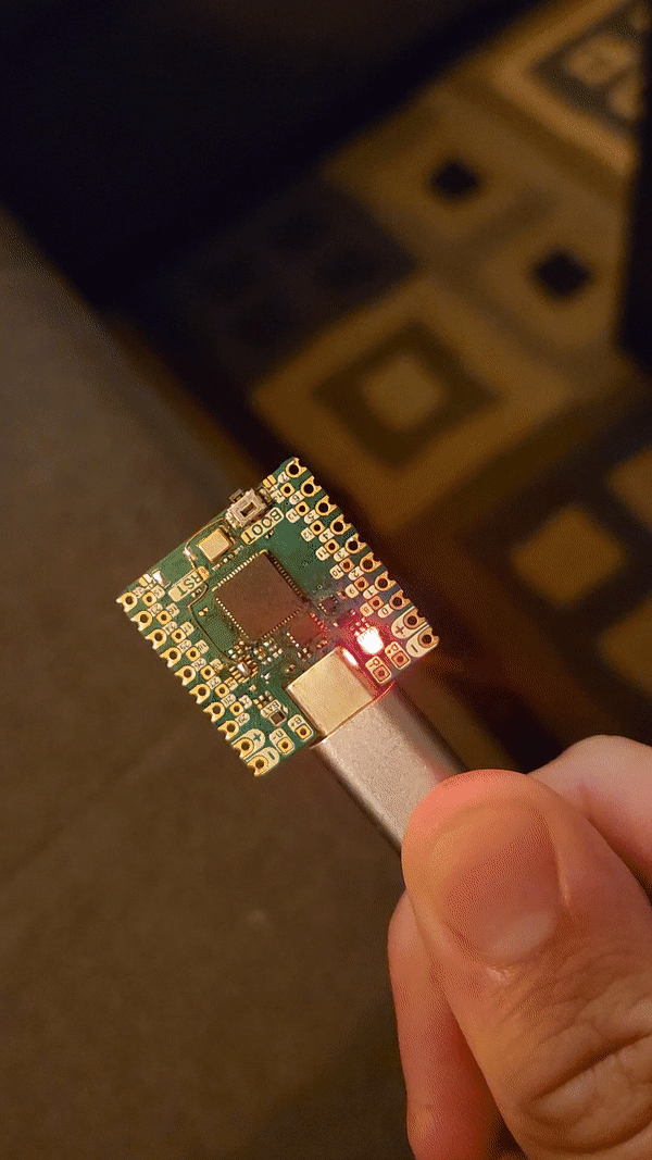
The real reason the CRAPi board started working is because I said screw it and tried programming it after fixing all these issues. Sure enough, it worked this time. Turns out it just needed the flash to not be entirely blank. The mass storage unmounted and stayed unmounted. More importantly, we got a BLINK!!!!
![]()
What's next??
A whole bunch of stuff. You'll notice that I didn't even test the LiPo charger yet (because I think there is something wrong with that circuit too!). But from there, it's just a matter of making some minor tweaks and then sending it off to PCBWay to test their services!
- Linear Regulator
-
Rev. 2 has arrived (and it works!)
08/09/2023 at 03:59 • 0 commentsIn the last log we suffered through the very first revision of the CRAPi board! That whole experience really lived up to this board's namesake. Not surprised, just disappointed. The first two logs were retrospectives. Rather than just jumping into where the project is now I wanted to make sure I showed the last few months of design and trouble shooting. The board became more and more unreliable until it eventually refused to enter programming mode. Making stuff is hard!
Thankfully, this post now brings us firmly into the present. I had decided to cut my losses with Rev. 1 and focus on moving forward. I started Rev. 2 in the middle of February and "finished" the design around the middle of July, with time spent on the project ramping up exponentially once the semester was over. All told that's about 5 months worth of work. So here's what changed in that time:
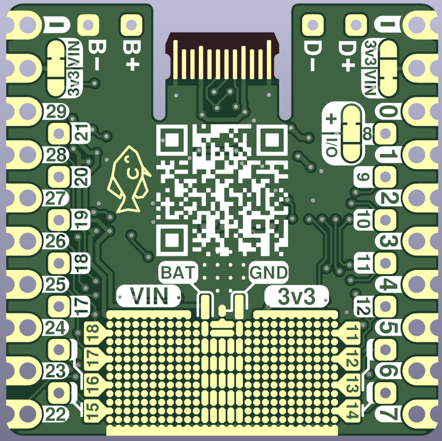
Changes in Rev 2. of the CRAPi2040
- Pin Labeling
- Went back to traditional silkscreen but used a "knock-out," negative-space style.
- Improvements to the ProtoGrid
- Pin pads that should let solder bridges form more easily
- Better GPIO Access
- Vertically oriented pads for 20 mil spaced surface mount connectors
- More prototyping space.
- Thad Improvements
- Increased the diameter of the center hole to match diameter of common jumper wire
- Bread board jumpers can now be (hopefully) friction fit into the Thads and/or soldered
- Right Angled buttons
- Low profile buttons hang off the side of the PCB
- Allows for boot mode and resetting even when the board is upside down
- Route-able Power Pins
- Solder jumpers let you route 3.3V or VIN to either side of the board
- Independent of each other - 4 total configurations for max flexibility
- Configurable Power LED
- Lets you reclaim the red power-on LED for RGB usage
- A second BLUE LED attached to Pin 25
- Blue LED attached to GPIO 25, so default Pico blink examples are (almost) drop in.
- RESET and BOOT button breakout jumpers
- Solder jumpers to route the BOOT and RESET buttons to GPIO pads.
- Gives an optional, general purpose user button (which seems to be pretty rare!)
- Can reset itself (which I guess could be useful!)
- Castellated Holes
- Allows for use on a breadboard and as a module on a PCB
- No components on the back of the board so no cut out needed.
- QR Code Link to Documentation
- Quick access to pinout documentation because those labels are tiny!
- LiPo Battery Charging IC (!!!!!!!!!!!)
- Single cell LiPo battery charge and automatic switching circuity.
- On board indicator of charging status via a second RGB LED.
- Oh god why did I decide to add another IC to this design.
How's that for 5 months worth of work?
With all these changes it also meant that I needed to start routing completely from scratch. This time I decided to drop the trace width from 7 mil to 5 mil as well as the size of the vias. Just for my own sanity I also changed all the passive components on the board from 0402 to 0201. Some may argue that this was just exchanging sanity in the virtual world for insanity in the real world went I went to assemble the things.
Routing Comparison
All in all I'd say that I did a much better job routing this time around. My main focus was keeping traces on the top layer of the board and ground plane in tact on the bottom of the board. Just for fun I also made sure that to length match the traces going to the flash chip and the USB lines, mostly because I like how the squiggly lines look. Rev. 1 is on the left and Rev. 2 is on the right. Not bad right?
Again, old on the right, new on the left. It gives you a pretty good idea how things changed and why it took 5 months to Rev the board!
You can also see that I had to give up the mounting hole... I determined that all the new features would be worth give it up. The board doesn't have any components on the back side so you can always double side tape it down. I am also thinking about making some sort of carrier board that would solder to the Thads specifically to add mounting holes. So many ideas so little time.
Cool Silkscreen HACKS!!!
Here are the obligatory KiCAD Renders. I spent a TON of time on laboring over the silkscreen labels on this revision. A huge peeve of mine is constantly looking up pin outs or counting headers to find the pin that I need. So instead of leaving that burden on the user of the board (future me), I put a half ounce more thought into my silkscreen labels.![]()
![]()
The real secret weapon to all of this was Inkscape. Pretty much part of the silkscreen was made in Inkscape, converted into a Path, then imported as a polygon on the sillkscreen layer. I would take a screen shot of the orthogonal 3D render, paste it into Inkscape, and then scale it to the dimensions of the board. That way I could create the silkscreen of one entire side in one shot, without needing to switch between softwares. When I was done, I only needed to perform a single polygon import.
You'll also notice that almost all of the text is in "knock out style." In other words, the text is written as negative space in the silkscreen. This is purposeful and is a great way to squeeze a little extra readability out of tiny silk screen labels. The advantages to the knock out style are two fold.
- Dark text with a light background is arguably easier to see and parse
- Imperfections / fuzzy edges are less impactful.
Point number one seems pretty intuitive, but I really had to think about point two. My explanation for this phenomenon is that it is much harder to deposit silkscreen precisely than it is to avoid depositing silkscreen. Additionally, such small amounts of silkscreen are most likely under deposited so the shape isn't really filling the outline that you want. This is actually advantageous for knock-out text because it "expands" the border of the text slightly.
Hopefully that makes sense.
RESULTS
Enough of this virtual non-sense, how did the boards turn out? Well, you tell me!
![]()
Oh, BABY! Isn't that just the most beautiful thing you've ever seen? After many long months, this thing turned out to be a work of art. Also notice what it's connected to!!! That's right
THE BOARD THICKNESS WAS CORRECT!
But I didn't want to get my hopes up too much. I figured that a good way to test if the pins of the board were making contact where they were supposed to was to cover the connector with dry erase marker, connect it, and see where the marker had rubbed off.
![]()
Sure enough, after connecting and disconnecting just a typical USB-C cable the results were almost perfect. The Ink was missing was perfectly removed from right on top of the pins. The pins inside the connector had made contact and wiped away the ink. The two outer most (and longest) are ground pins which makes sense. The next two inner most, and slightly longer pins are the D+ and D- pins for the USB.You'll notice that there is a bonus 5th pin that has been wiped clean as well. Initially I thought that the pins were making uneven contact which is why some some of the pins were wiped and others were not. Then I looked inside my USB-C cable and oddly enough not all of the contacts inside the connector are populated. So everything looked exactly how it was supposed to! The ink also reveals that the contacts are making contact with the PCB a reasonable length down the trace.
I don't see a reason why this connector can't sustain a USB connection given the positive results above, but we won't know for sure until I am able to program a fully assembledHOW ABOUT THAT SILKSCREEN?
The other thing I was most excited to see was whether my theories on the knock-out style silk screen were valid. At first glance with the good 'ol eyeball it seemed like hypothesis was true: knock-out / negative-space labels can be more reliably read than their positive-space counter parts of the same size.
![]()
![]()
![]()
Looking at the labels under a literal microscope, they don't look great. But from a distance they are way better than the silkscreen on Rev 1. Most importantly, it's good enough for my phone to read the QR code on the back! I wasn't sure if that was going to work or not
Even with these tricks though, the poor quality of the JLC silkscreen is pretty apparent. Even worse, the silkscreen seems to be pretty inconsistent. Out of the 20 boards that I ordered, there was pretty wide range of "weights" for the silk screen with either very thick white layers being deposited or very whispy thin layers. I wouldn't really mind the undefined edges, but the inconsistency makes it really hard to account for. I think that in my next inevitable revision I will try PCBWay to see if their silkscreening process is higher resolution... or at the very least more consistent.And there you have it! Pretty short log for today. In the next one I will finally put one of these things together!
- Pin Labeling
-
Rev 1. PCB Assembly!
08/08/2023 at 04:34 • 0 commentsAlright here we go! In case you missed the last log, here it is! Check it out because what you're about to see will make a lot more sense. Just like the last log, this log is going to be a retrospective, but I promise that the next CRAPi2040 log to grace your retinas will be firmly rooted in the present!
We left off with the very first "completed" revision of the CRAPi2040 board. All told it probably took a few tens of hours to design and layout. Some of that time included picking out parts, learning KiCAD, and looking up reference material. But I would say that 75% of that time was for sure spent routing and rerouting traces and trying to keep my ground plane in tact. I'm going to be honest, the amount of time I spent laboring over that routing was probably not healthy considering I was supposed to be taking a break from school and only focusing on work and my friends and family.
But who cares about all that stuff. You're here to see that gorgeous board! So here it is!

Beautiful I know, even if my phone camera washed it out a little. You can get a really good look at the routing thought which I think is awesome. You'll notice that I didn't do a great job at keeping my traces on the top of the board so some current paths are probably longer than they need to but on a board that is only 1 square inch probably not a huge deal. To be honest, it looks a little crappy to me but hey sometimes you've just got to send it. The gerber files that is, to JLCPCB.
If those pictures don't satisfy you, say no more. I am lucky enough to be the proud owner of a garbage bin microscope! It's sort of hard to take good pictures with my phone through a microscope but it's better than nothing. Plus it's a huge help when trying to deal 0402 components. My eye sight is pretty good but this really takes a lot of the guess work out soldering these leadless components. To the surprise of no one, it's hardly smooth sailing from here so I'll take every advantage that I can get.
At a first glance under the microscope things look GREAT. I didn't really know what to expect from JLCPCB because these boards were literally 20 cents each. The driving factor for such a low cost board, as you may have noticed, is that I went with a HASL finish on the copper pads. This was my first time even hearing about the process so I needed to look into it.
HASL stands for Hot Air Solder Leveling and the process basically involves dipping the entire circuit board into a vat of molten solder to tin the exposed copper. As the board is withdrawn all the excess solder is blown away by hot air knives. Or so I am told by Google. Looking at picture definitely helped.

This is opposed to the typical ENIG (Electroless Nickel Immersion Gold) process that most "normal" PCBs are put through. This is the one that gives you those nice shiny gold pads. The ENIG process deposits a layer of nickel and then a layer of gold on to all the exposed copper, without using an electric current. Nickel is essential for preventing the gold from diffusing into the copper and of course the gold is great to solder to and provides corrosion resistance. But obvisouly the most important part is that ENIG is prettyyyy.
 The (G) stands for (G)old so it's cleare why ENIG would cost more money than HASL. When I sent the boards away I already knew that I was going to need to do another board revision so I didn't bother getting the good stuff. That turned out to be a great choice considering all the issues these boards would have. I'm not surprised, just disappointed.
They Thicc.As a reminder, the PCBs need to be around 0.7 mm for this crappy USB-C connector idea to work. The closest option available was 0.6 mm from JLCPCB so it wasn't even a given that these boards would work. Unfortunately, we would not get to see if that 0.1 mm really made a difference because the PCBs that were sent were 1.6 mm!
![]()
It's pretty easy to tell that is way thicker than we wanted but just to really send the point home here is a comparison picture of a "tongue" that is the correct thickness.
![]()
So I was super bummed about that. I thought that for they had made some sort of mistake in my order. I mean this idea was the whole basis for this project in the first place! Surely I couldn't have made the mistake! Yeah well, a quick visit to the JLCPCB invoice showed that I did actaully order 1.6mm by mistake. When I was ordering these boards it was probably about 3 a.m. and I had reuploaded a few times. I thought I was careful to select the thickness but I guess the lack of sleep got the better of me.Lesson Learned: Don't order PCBs after midnight.
Through manly tears and gritted teeth I told myself I could still make the most of it. Thankfully I had broken out the USB D+ and USB D- lines on the RP2040 so that I could still program the board with a chopped up USB cable. Plus, there were still plenty of other things to check out!Solder Mask not Silk Screen
One of the things that I was most interested to look at was the resolution of the text in solder mask versus in silk screen. I had a feeling that the JLC silkscreen would not be fantastic considering the price. I'm workign with a pretty limited amount of board real estate and so I knew that the pin lables would end up being pretty tiny. I also had a feeling that the resolution of the solder mask would be far better than the silk screen. I turned out to be right!
![]()
![]()
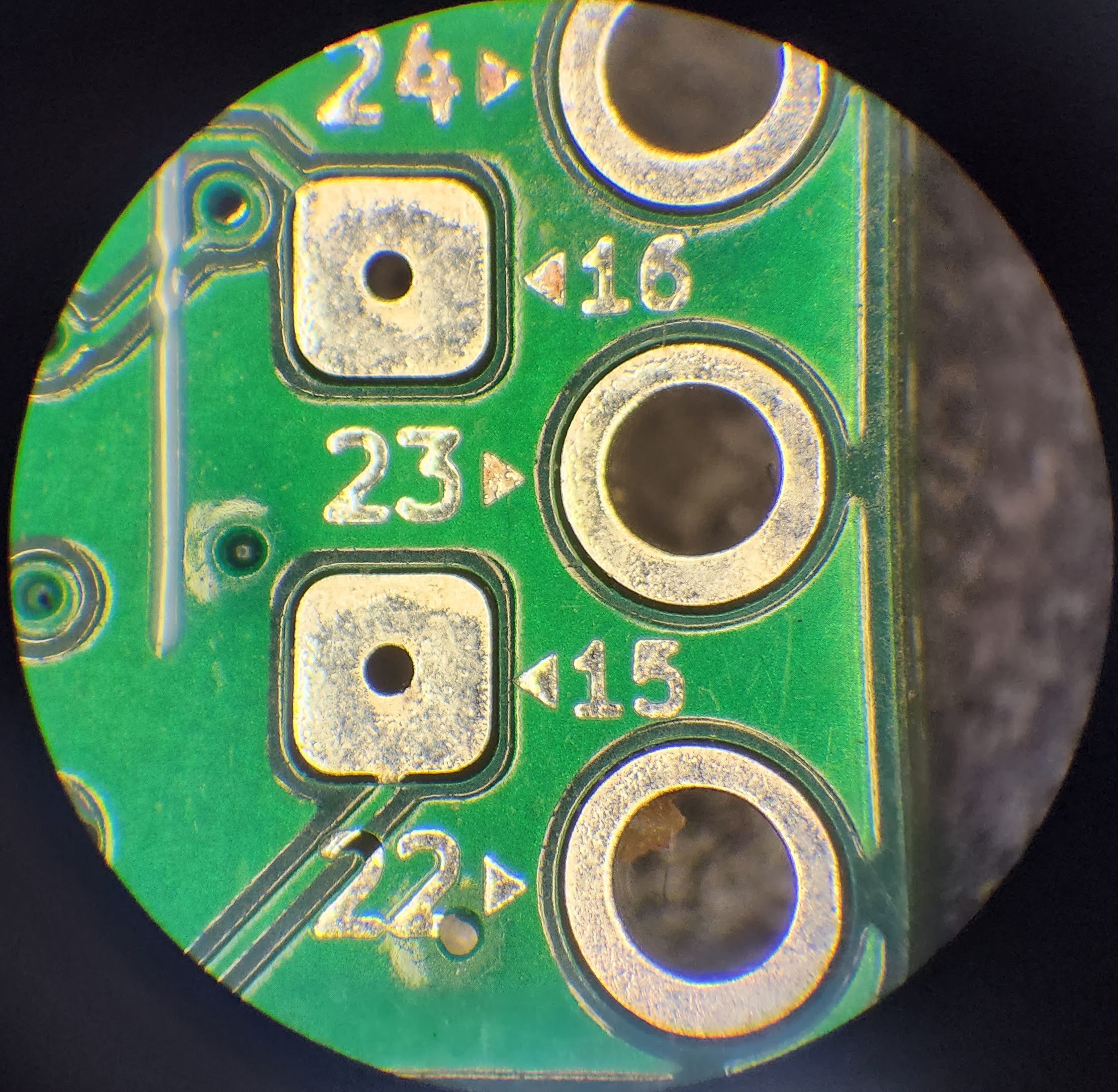
I was surprised to see how just how chunky the silkscreen looks under the microscope. Granted, this isn't particularly high quality silkscreen, but still. The name of the game here is cheap, remember? It's just a reminder that you get what you pay for. The solder mask text looks far far better. The text size of the "23" is 1 mm if I remember correctly and the size of the "15" is 0.75 mm. But if we turn off our microscope the story is a bit different .
Taking a look again at the phone picture, you'll noticed that the numbers aren't super readable. That's not just a result of the crappy picture. In real life, the numbers are actually pretty hard to see. This is because the HASL process that we talked about earlier leaves a nice shiny silver coat of solder on all the exposed copper of that board. Tiny silver letters don't show up well with a green background. If I had gone with the more expensive ENIG process I am sure that the letters would be been much more legible. Ironic.. You can see that the BOOT and RST text worked a bit better because they are bigger, but still not ideal. The BOOT and RST text also highlight another issue with putting text in the solder mask: you need to sacrifice a lot of ground plane. I got lazy towards the end so I wanted to see what vias would look like when placed in the solder mask text.
Evidently you can push text-in-solder-mask pretty far! But text this small quickly becomes useless to the naked eye. I guess you can leave secret messages for microscope owners though!
Lesson Learned: Under certain conditions, putting text in solder mask can be a good way to get around silk screen issues.
For this board though, it didn't really work out. With the next revision, it was clear that I was going to need as much space for traces as possible. I couldn't really afford to waste space with labling. Although, under the right conditions I'd love to try this trick with an ENIG board, so I will keep this trick in my back pocket.
Looking at the ProtoGrid and Thads
I'd say that both the ProtoGrid and Thads turned out pretty well too! You can see that the GPIO labels for the ProtoGrid connections are visible under the microscope but almost invisible to the naked eye which is a bummer. I did incorporate a nice little trick for keeping tiny pads stuck down though, and that's to drop a via in them. You won't be able to (and shouldn't!) do this for most l pads but in this case it made sense and made a big difference in pad durability. I didn't show it here but even after some casual testing the pads without vias on the grid came up very very easily. So it's pretty clear that in later revisions I would need to try to make them a bit bigger so they don't just flake off under a soldering iron. I was feeling a bit discouraged at this point so I didn't really test the Thads but I'm still convinced that they will work and will test then in Rev. 2!
TIME FOR ASSEMBLY
Alright, that is enough inspection. Let's put the thing together and see if it actually works! This post is already getting pretty long so I am going to kind of cruise through some of this stuff.
First question is: to solder paste or not to solder paste? With all of these 0402s and non-leaded components I chose to solder paste, at least initially. I also got myself one of these.That's not my hand by the way.
It's a positive temperature coefficient (PTC) hotplate that heats up to +300C (in other words hot enough) as soon as you plug it into the wall. The nature of the PTC heater inside the piece of extrude alumnium means that it regulates it's own power output. For the circuit building snob this is no replacement for a proper oven or hot plate that can execute carefully controlled reflow profiles. For me though, falls firmly into the "crappy but useful" territory I have come to know and love. Plus the thing only costs like 15 bucks, so it's really hard to complain. It melts my solder and that's all I can really ask for.
This did come back to bite me a bit though, more in the Rev. 2 post about that.
Turns out, the stencil that provided by JLCPCB wasn't really suitable for this fine of work. It was too thick which meant that too much solder paste would be applied to the pads of the PCB. I was able to mitigate this somewhat but placing the populated PCB on the plate and then plugging it in so that it more gradually got up to temperature.
Ultimatly though, the HASL turned out to be a good move. With so many solder bridges I gave up on the paste and just stuck components to their pads with lots of flux. The little bit of solder on the pads from the HASL process was enough to form good connections with most of the components. I could then go through with a little bit of paste more selectively, and fill in any missing connections via soldering iron and microscope.
Lesson Learned: Paste is not always the answer for SMDs!With the construction method sorted, I finally started getting some parts on to the boards!
Linear Regulator Woahs
It's worth noting that I did take somewhat of a systematic approach when first assembling the board. The first chip that I needed to prove out was the linear regulator that drops the 5V to 3.3V. I choose the MIC5528-3.3YMT-TR because this thing is TINY. The datasheet says 1.6 mm by 1.6 mm. The datasheet also says that it can push out 500 mA, assuming you don't mind a crazy high junction temperature and almost immediate thermal shutdown.. Realistically, 100 mA of continous output is more reasonable to expect from this chip but it's nice to know that it won't brown out if there is a current spike.Yep, those are the tips of tweezers right ther. This thing is small and I wanted to make sure tot do a REALLY good job NOT shorting out pads when I was reflowing. For some reason though, they kept getting burning hot when they were hooked up. I was convinced that I was shorting the pins or that I had gotten the footprint wrong because every single LDO suffered the same fate. Well turns out my reflowing was totally fine.
I know it might not seem like it, but my connections to the LDO on the left hand side of the board were NOT the problem. So look hard and see if you can spot why all of the LDOs that I soldered to this board were dying a firey death. Give up? Don't worry it took me a while to spot too.
Once again I experinced that feeling of trying to be too clever for my own good. The "+" is created by a lack of solder mask on the ground plane. I thought I was so clever with this nice little plus sign (see above). The pad directly next to it, the one whose function it is describing, is of course the 3.3V RAIL. I had solderd jumpers on to the 3.3V pad to make sure I wasn't trying to probe through oxidation or flux. I had inadvertently bridged that < 1 mm gap with solder and didn't even notice... making a dead short between ground and 3.3V. It's funny how the steps that I took to be careful with my measurements ended up making my life harder.
Lessons Learned: Don't be too clever for your own good. and honestly so many more.
Mo' Flash Mo' Problems
Feeling pretty silly about myself, but getting a nice 3.3V from my LDO all the same, I pushed on. With the power sorted I moved on to the clock crystal, LED, and RP2040. Making sure to savor each little victory. We got a clock signal on the 'scope, a glowing red LED, and most importantly: A RP2040 MOUTNING AS MASS STORAGE!!!!! LET'S GOOOOOO!
With my spirts flying high I dragged and dropped a blink.u2f file on to the Pi and after a second the drive disappeared. OUTSTANDING. I'm on top of the world right now thinking about how awesome it will be to have my very own dev board and then disaster!!!!
Only a few seconds after dragging and dropping that file the RP2040 REAPPERARED???
That's pretty odd, surely that must mean it's a flash issue. I had this same behavior when I tried to power on without the flash chip installed. I figured that I had probably had just bridged a pad on the flash chip. A few reflow attempts later and no dice. The RP2040 was inscently presenting itself to the computer.
Just to be sure that I had all my connections right I under took the dead bugging of my lifetime. Thank goodness for the microscope and that I didn't drink any coffee that day. And by the way, that's not enamaled magnet wire. Those are individual strands of copper wire that I pulled out of a bread board jumper cable. Yeah this was not a fun day.
With my flash deadbugged, and my board crusty and dusty but outputting 3.3V and a clock signal I was ready to make that LED flash and for the RP2040 to stop resetting itself and........... NOPE. Even with the beautiful PCB that you see below it, was the exact same story. The RP2040 would mount as soon as I plugged it in, regardless if the BOOT button was held down, disappear briefly when I gave it a file to eat, but then come back a few second hungry for more.
At this point I was beyond frustrated. The symptoms seemed to indicate that the flash was not being detected for some reason. Now that I was 100% that everything was connected correctly in the real world, that must mean there was a problem on a virtual world of design. Surely I couldn't have made a mistake in the schematic, right? I mean the flash connection is so straight forward! Yet again, to no one's surprise. I was wrong.
Taking a look at the schematic from the Raspberry Pi Pico, you can see that the QSPI_SS signal is clearly connected to both the button and the RP2040. I had missed that connection on my schematic. The flash chip was only connected to the button. So without the ability to strobe the CS pin on the flash, the RP2040 didn't detect that the flash was even connected, thus giving me the behavior I was seeing.
Lesson Learned: Never overlook "simple" connections
Once I had installed the approriate bodge wire the RP2040 no longer thrust itself at my computer's file system, which is the good news. The bad news? I was never really able to get a fully functioning board on the this revision. Getting the RP2040 to mount ended up being unreliable and I sort of got an LED to blink once or twice but it was nothing worth showing.
By this time grad school had started back up and my day job was burning me out too much to keep pushing with this revision of the board. Demoralized but not devestated, I was determined to make Rev. 2 a success! As soon as finals were done of course....
Sorry for the long post, and I wish that I could ended better for this revision. but fear not! In the next post we will see Rev. 2 and that ladies and gentleman is an outstanding success which will finally catch us up to real time.
If you made it this far. I am very proud of you, just remember the best is yet to come!
- (C)hris -
Rev. 1
08/05/2023 at 04:06 • 0 commentsThis is going to be somewhat of a retrospective. Over the past year I have been working full time and have been concurrently completing my graduate degree as a full time student . It's been a lot of work so if things get a bit disjointed in the narrative that may have something to do with it. I've got like, two brain cells, so this has not been an easy project!
The intro may not have made it clear but this was supposed to be a weekend project for a quick, all purpose, dev board of my own. I was shooting for a half step above breakout board for the RP2040. With that in mind a primary goal was to break out ALL the pins. On the stock Raspberry Pi Pico you only get access to 26/30 GPIO pins. I'm paying for 30 pins of GPIO so gosh darn it I want to use all 30 pins if I feel like it! That's of joke of course, I'd be sick of layout too after spending who knows how long laying out custom silicon.
But then my cheap brain cell gets all worked up with this lofty pin-breakout-goal presented by the flexible brain cell. Why? Because more signals means more pins, which means more board area, which means more money! So the first question was: how small can I make the make the board. The second question was: how could I break out all the signals in a reasonable way?
The answer to the first question was clear: I'd make it 1 square inch. Why? Well that's the size of the RP2040 Stamp, which I'd argue isn't really a development board and more of a daughter board or maybe an SoC. Sure it's technically hand solderable but what's the point if you need a carrier board to even use it? Then it's no longer 1x1 inch!
Answering the second question was a bit more difficult. After many minutes of thinking my two brain cells presented me with:
The Thad - A Through-Hole Pad.
Clever name, I know. Hopefully a clever solution too. It's literally just a square pad with sort of small plated through hole down the middle
Yep! That's all it is! But sometimes the simplest solutions are the best solutions. Obviously this gives you a nice place to solder jumpers, but more importantly, it also allows you to hand solder the board down another circuit board without having to deal with the 2mm pitch of the RP2040 Stamp. The hope is that if everything is tinned properly then the solder will follow the heat down the plated hole and be drawn onto the bottom pad through capillary action. I don't really know what capillary action is but it sounds applicable in this case.

Through Hole Pads = Thads! Space those bad boys out on a 0.1 inch grid and stagger them with the regular header pins and it feels like just maybe we found a cool solution. There's one more cute little trick that I'll show in the next post that really takes this concept to the next level, so stay tuned.
Alright great! So we have the Thads taking care of breakout duty but man, my cheap brain cell wasn't quite satisfied. I mean sure, those pads don't technically cost money, but look at all the space they are taking up! We're only working with one square inch here, buddy! We better do some serious space saving somewhere else. And oh boy did we save some space in promote the most questionable way possible. Presenting:
Free USB-C Connector - USB-C, but SKINNY
If you think about it. What do you really need in a USB-C port? Obviously you'll need the metal contacts because electrons tend to flow better through metal. Or so I'm told. You'll also need something for the metal to sit on, so substrate material is pretty non-negotiable too. The rest? Well, do you really need it? "Strain relief something something," I hear you mumble; but do you really need it. You may say yes, but I say no!
Hear me out. For something like a phone or a laptop, of course this would be a horrible idea. You would snap this little piece of fiberglass off in an instant as soon as you forget your phone is plugged and try to roll over while reading Hackaday in bed. Ports for consumer applications like that need to survive potentially thousands of mating cycles and all sorts of wear and tear. The port on a microcontroller? Not so much. If some how you manage to wear out the connector on a CRAPi board, with a few hundred mating cycles, congrats I guess! Thankfully for the more enthusiastic USB users, the CRAPi2040 breaks out the USB lines of the RP2040 to 0.1 inch header.
With our trimmed down USB-C connector, we save precious board real estate and frustration with the soldering iron. Interestingly, I haven't really seen this done before. There is this project from a few years ago using Eagle (RIP) that attempts to create a PCB USB-C connector but there was never a report of success. So I certainly won't say that I am the first one to attempt this idea, but it seems like I might be the first one to attempt this idea on a development board.
Section 3.2 of the USB-C Spec describing the Tongue :p You might say it's a bad idea, or a crazy idea, maybe even a crappy idea. Thankfully, I am willing to push the boundaries of crappy ideas so that you don't have to. So I spent some time studying Section 3.2 of the "Universal Serial Bus Type-C Cable and Connector Specifications," also so that you don't have to. The result? The beautiful KiCAD footprint that you see below, which is designed to be integrated into the Edge Cuts layer of the board outline. I think it looks pretty slick.
3D View of Edge Connector (just imagine it's part of a larger board) Of course making something on the computer is easy, but making something in real life is way harder with all of those pesky atoms. The real tricky part here is going to be the ever mysterious Z-axis i.e. the thickness of the PCB is going to have to match the thickness of that little tab (or "tongue" as it is officially called, which I love) inside the USB-C connector housing. If you have a phone or device with a USB-C receptacle on it I encourage you to take a look inside and guess how thick that little thing is.
Ready for the answer? Wanna look again? It's 0.7mm. You would know that if you read the spec!Thankfully, JLCPCB (because who else would I be using for this project?) gives the option for a 0.6mm board with some limitations on layer counter and silkscreen color. The color is for sure a bummer, but considering the journey that I was about to embark on I really wish I had the option for a 4 layer board. With ideas this crappy, sometimes the only option is to just push through with spit, grit and a whole lot of time routing traces in KiCAD. (spoiler: the connector it worked. If you have read this far then you deserve to know!).
While I thought the cheap and flexible brain cells had finally settled down, I was wrong. They both wanted one last tribute. Sure, fine, I can do that! I promise that it will be a border line crappy idea that might just be good enough to be useful. Remember, the name of the game is to add "free" features through PCB design. How can we make the board as useful as possible without making it more expensive? That's where the third crappy idea comes in: the Protogrid!One of the many iterations of the Protogrid! It's literally just an array of tiny pads that are laid out on a 20 mil grid. The idea here is that half the time I'm using a dev board, I might just be interfacing with a single chip and a handful of passives. A great example would be a project using a CAN bus where all I really need is a CAN transceiver. Why wire up a whole bread board just for a single chip when you could just solder the chip right to the dev board. Then it's all ready to integrate into an enclosure.
There is some logic to the pad spacing and functions too. I found that a 20 mil grid should be the most useful as a lot of surface mount chips have leads that are separated close enough to a multiple of 20 that you can get clean connections. Pins 1 - 8 are connected to GPIO. Pin 9 is VIN (5V), Pin 10 is 3.3V, and Pin 11 is GND. The vertical pads running down the middle are spaced in such a way that if you want to solder on a new USB port you can do so as most of them of 20 mil pitch on their surface mount leads. See? Options!
Miscellaneous Features and Rambling
The three major points listed above are really just part of the picture for this first revision. On the second revision you'll see that I pushed the boundaries even further. For this board spin though you'll see a few other cool features:
- RGB LED because it turned out to be the cheapest LED overall on Digikey?
- Lettering in solder mask instead of silkscreen for better resolution at smaller sizes
- Power enable and disable jumper just for giggles
- A single 2mm mounting hole
- 0402 Components (not cool, just bragging).
- A boot AND a reset button so you don't have to keep power cycling!
The (virtual) reveal.
If you read this far you deserve yet another reward (you didn't just scroll to the bottom, did you?). Below you can see a virtual picture of the completed board. All of the supporting components to the RP2040 were chosen to be as small and/or as cheap as possible.Complete Render of Rev. 1
The eagle-eyed among you may have noticed that there is a discrepancy in the Protogrid between the KiCAD footprint picture and this render. That's my bad! Remember, this is a retrospective and my documentation skills aren't exactly on par. I forgot to take a better pictures of this first revision so the best I could do was the renders from my JLCPCB order.
Lucky for you, because this is a retrospective that means you don't have to wait very long for the next post to show you how Rev. 1 of the boards turned out. As you can probably guess... there were some major issues....
That's all for now, stay tuned!
- (C)hris


 Again, to my surprise: the footprint worked perfectly. The front anchor tabs of the connector have no problem being soldered down to the GND rail at the bottom of the ProtoGrid. I'm pretty sure I was designing this on a train to Chicago in the middle of the night. So, I don't really remember designing this, but I am glad it worked out!
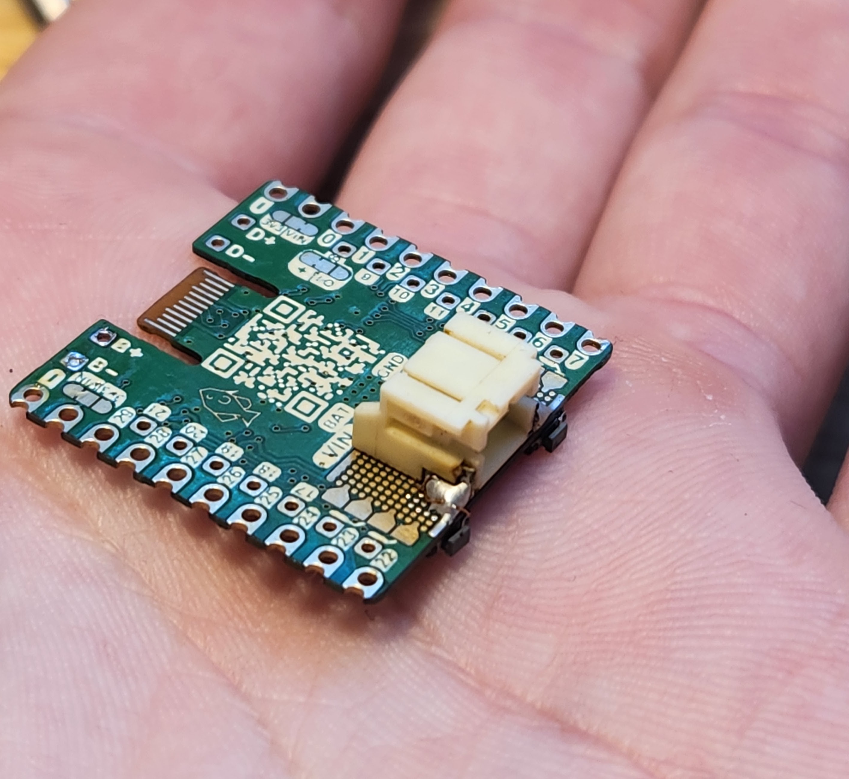
 Again, old on the right, new on the left. It gives you a pretty good idea how things changed and why it took 5 months to Rev the board!
 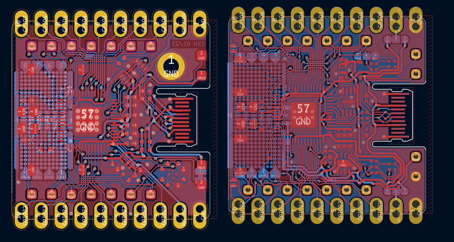 You can also see that I had to give up the mounting hole... I determined that all the new features would be worth give it up. The board doesn't have any components on the back side so you can always double side tape it down. I am also thinking about making some sort of carrier board that would solder to the Thads specifically to add mounting holes. So many ideas so little time.
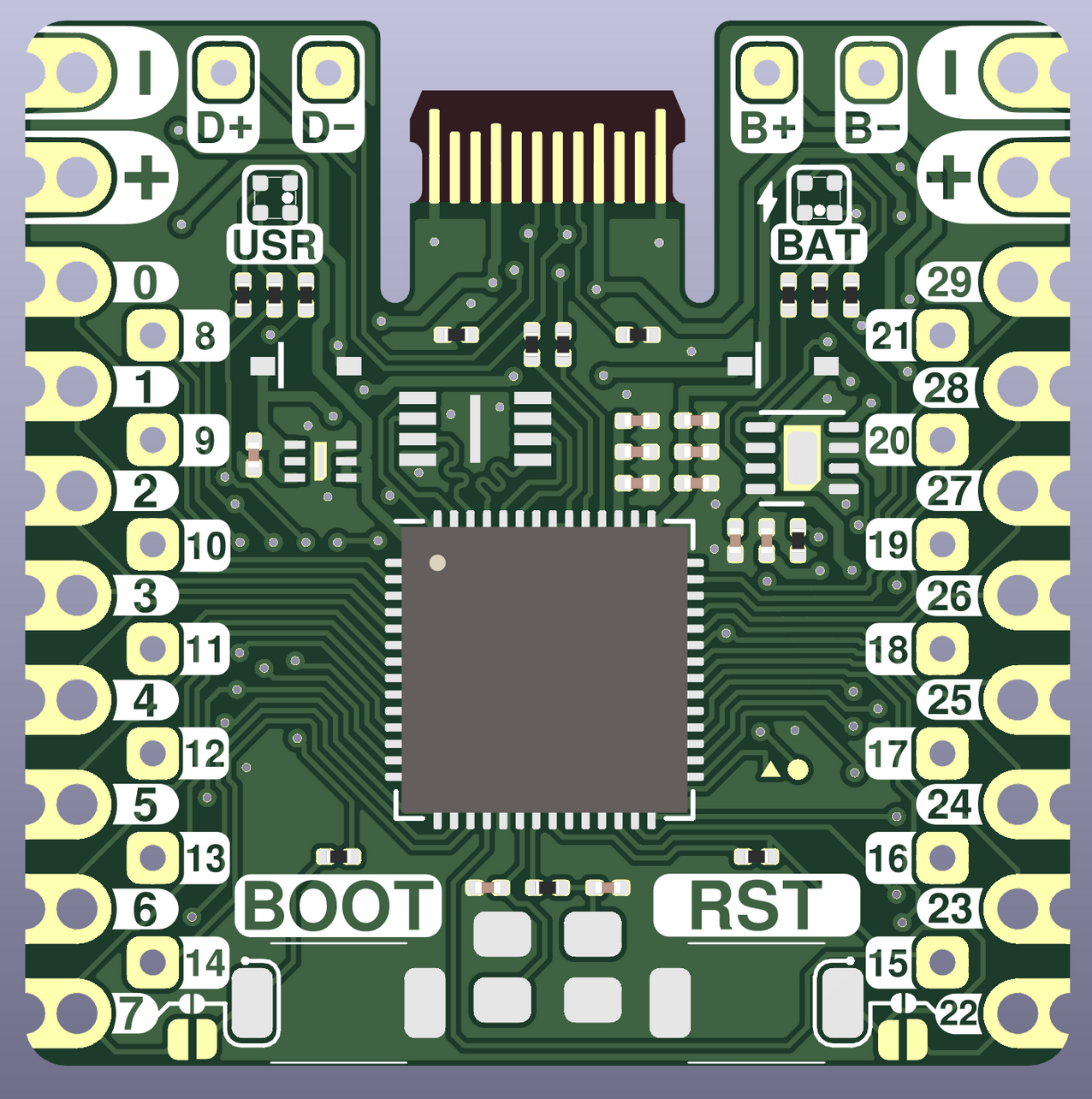
 You'll notice that there is a bonus 5th pin that has been wiped clean as well. Initially I thought that the pins were making uneven contact which is why some some of the pins were wiped and others were not. Then I looked inside my USB-C cable and oddly enough not all of the contacts inside the connector are populated. So everything looked exactly how it was supposed to! The ink also reveals that the contacts are making contact with the PCB a reasonable length down the trace.
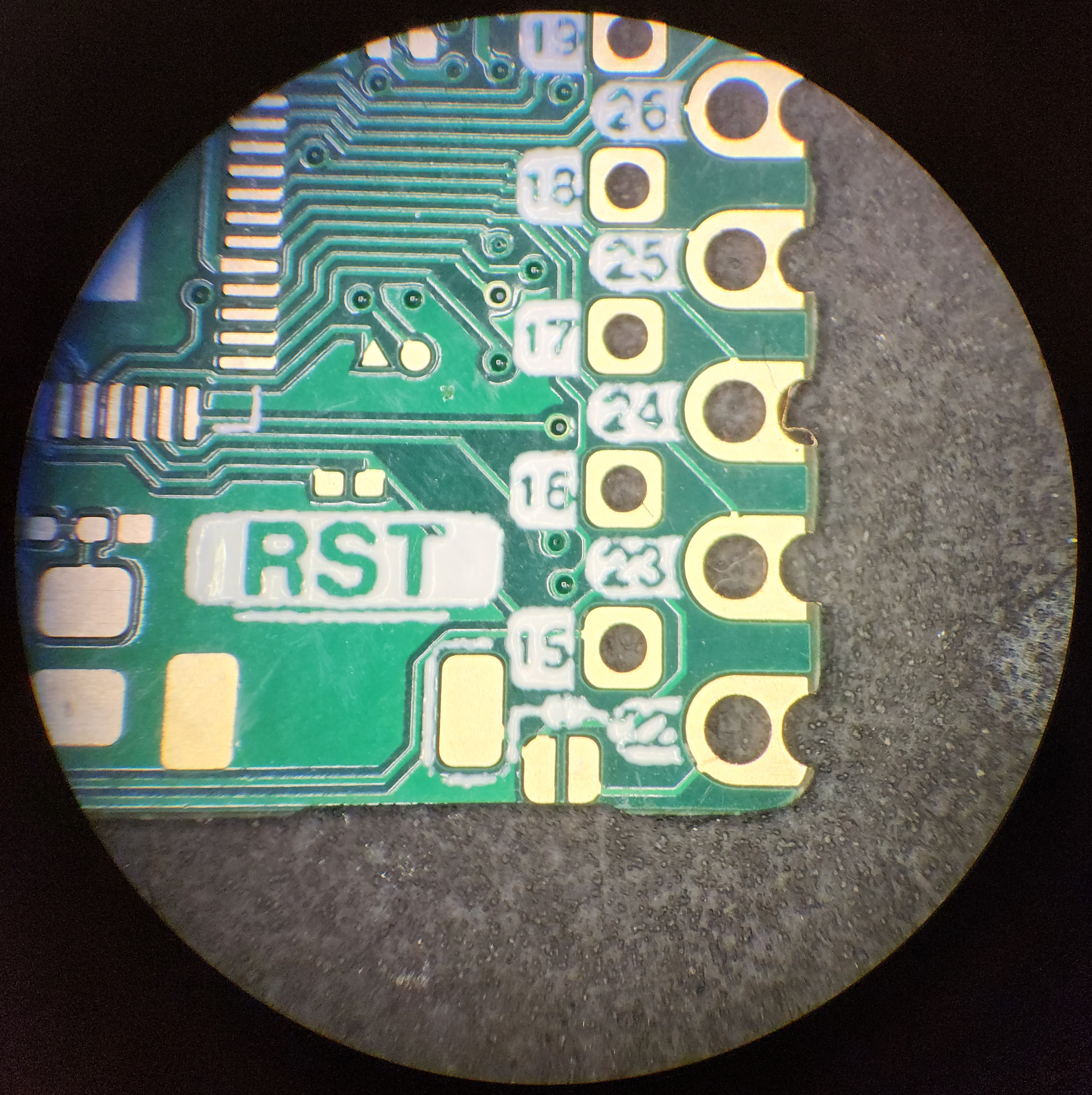


 The (G) stands for (G)old so it's cleare why ENIG would cost more money than HASL. When I sent the boards away I already knew that I was going to need to do another board revision so I didn't bother getting the good stuff. That turned out to be a great choice considering all the issues these boards would have. I'm not surprised, just disappointed.
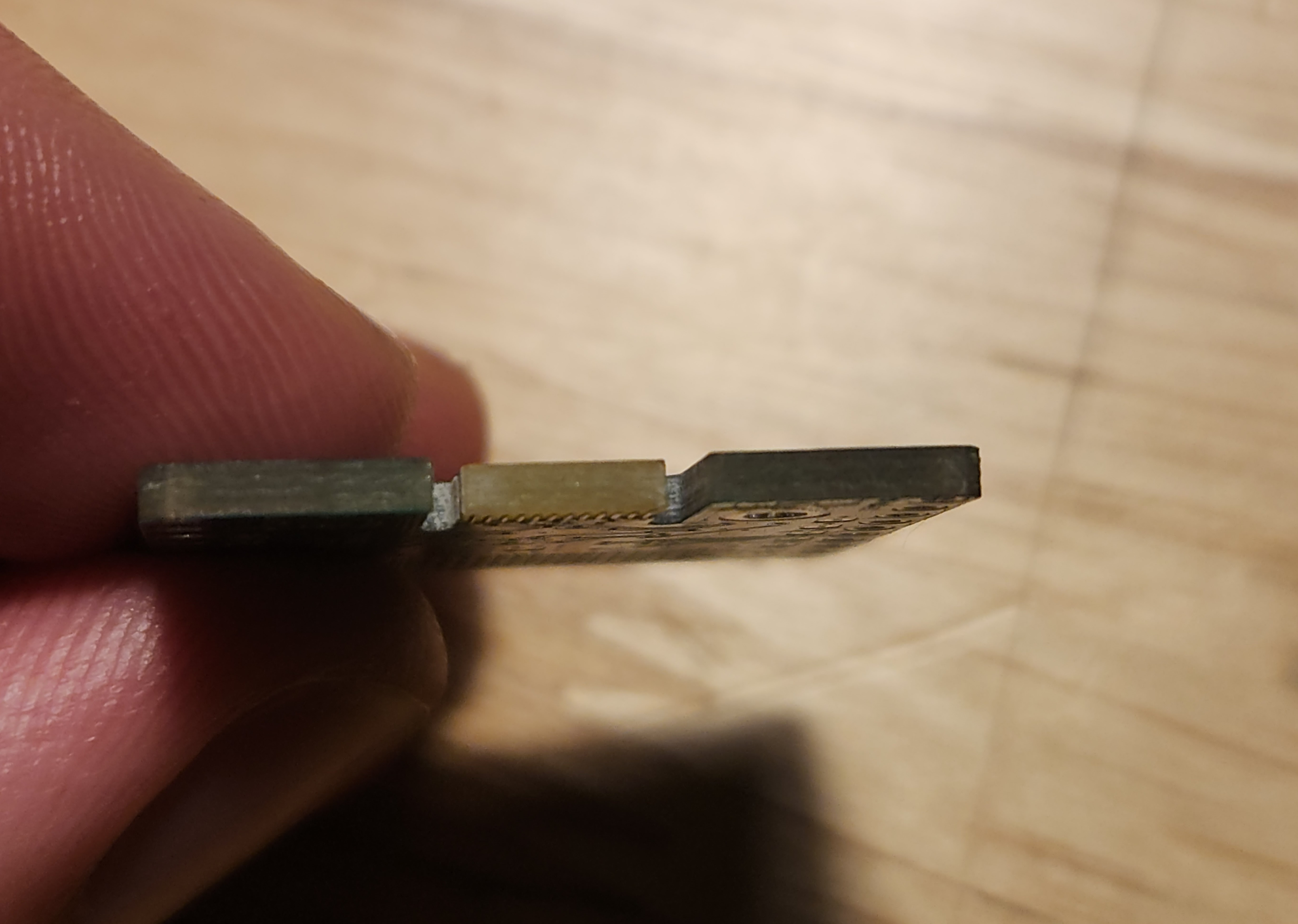


 That's not my hand by the way.
 I know it might not seem like it, but my connections to the LDO on the left hand side of the board were NOT the problem. So look hard and see if you can spot why all of the LDOs that I soldered to this board were dying a firey death. Give up? Don't worry it took me a while to spot too.
 Once again I experinced that feeling of trying to be too clever for my own good. The "+" is created by a lack of solder mask on the ground plane. I thought I was so clever with this nice little plus sign (see above). The pad directly next to it, the one whose function it is describing, is of course the 3.3V RAIL. I had solderd jumpers on to the 3.3V pad to make sure I wasn't trying to probe through oxidation or flux. I had inadvertently bridged that < 1 mm gap with solder and didn't even notice... making a dead short between ground and 3.3V. It's funny how the steps that I took to be careful with my measurements ended up making my life harder.

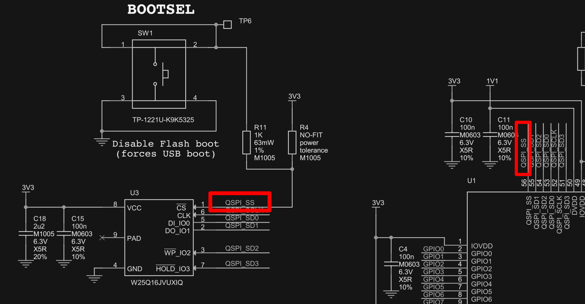


 Thankfully, JLCPCB (because who else would I be using for this project?) gives the option for a 0.6mm board with some limitations on layer counter and silkscreen color. The color is for sure a bummer, but considering the journey that I was about to embark on I really wish I had the option for a 4 layer board. With ideas this crappy, sometimes the only option is to just push through with spit, grit and a whole lot of time routing traces in KiCAD. (spoiler: the connector it worked. If you have read this far then you deserve to know!).

 The eagle-eyed among you may have noticed that there is a discrepancy in the Protogrid between the KiCAD footprint picture and this render. That's my bad! Remember, this is a retrospective and my documentation skills aren't exactly on par. I forgot to take a better pictures of this first revision so the best I could do was the renders from my JLCPCB order.