Dominic Emond-Belanger
-
Putting the project on hold for now
03/30/2024 at 18:16 • 0 commentsHello everyone!
This is a quick update to let you know that I had to put this project on hold for the time being. Due to some life change since the beginning of 2024 I had loss my working area to make space for our new baby.
We are planning to build a new extension for our home this year and I planned to build a new workbench in the new space to continue my electronic projects.
I will be back as soon as possible! :)
Cheers!
-
Mistakes where made…
12/16/2023 at 19:15 • 0 commentsA quick update after a 3 weeks break!
The processor board is fully built and I was able to free run the CPU without being connected to the motherboard. I already found some improvement to be done on the next revision :
- Move the GAL chip use to generate to act as a 82284 Clock diver and the 82288 Bus Driver to the motherboard chipset.
- Add some pins header along the edge connector to give me easy access to all the signals for debugging.
![]()
Processor board v0.3 The next step was to populate the motherboard and began the work on the CPLD in Quartus.
![]()
![]()
![]()
![]()
It was the time for the big test... and it didn't go well..
The first issue was a huge short on the power rail, I found out that my VCC and GND pins on my edge connector where flipped. To be sure I looked back the schematics and confirmed that the A and B sides of the connector where not flipped :
![]()
![]()
Then I realized that the footprint that I used was wrong... the A and B sides where indeed flipped and where mislabelled!
So now that I know the issue, I need to take a decision if I spin a new revision for my processor card or if I do a workaround for now in case I found more issue before ordering a new board.
I worked on the revision v0.4 of the processor board, I fixed the edge connector, added the pins headers and remove the GAL. I still need to integrate the 82288 bus controller in my chipset later.
![]()
Processor board v0.4 Before ordering this new revision, I want to do more test on my current v0.3 revision if possible. I have ordered a PCI extension that I will re-wire to be able to use my v0.3 board and make sure that I do not have other issue with the design.
![]()
Next steps
- Make a workaround with a PCI extension to be able to test the current v0.3 board.
- Integrate the 82288 bus controller in my chipset.
- Make a new processor card revision.
-
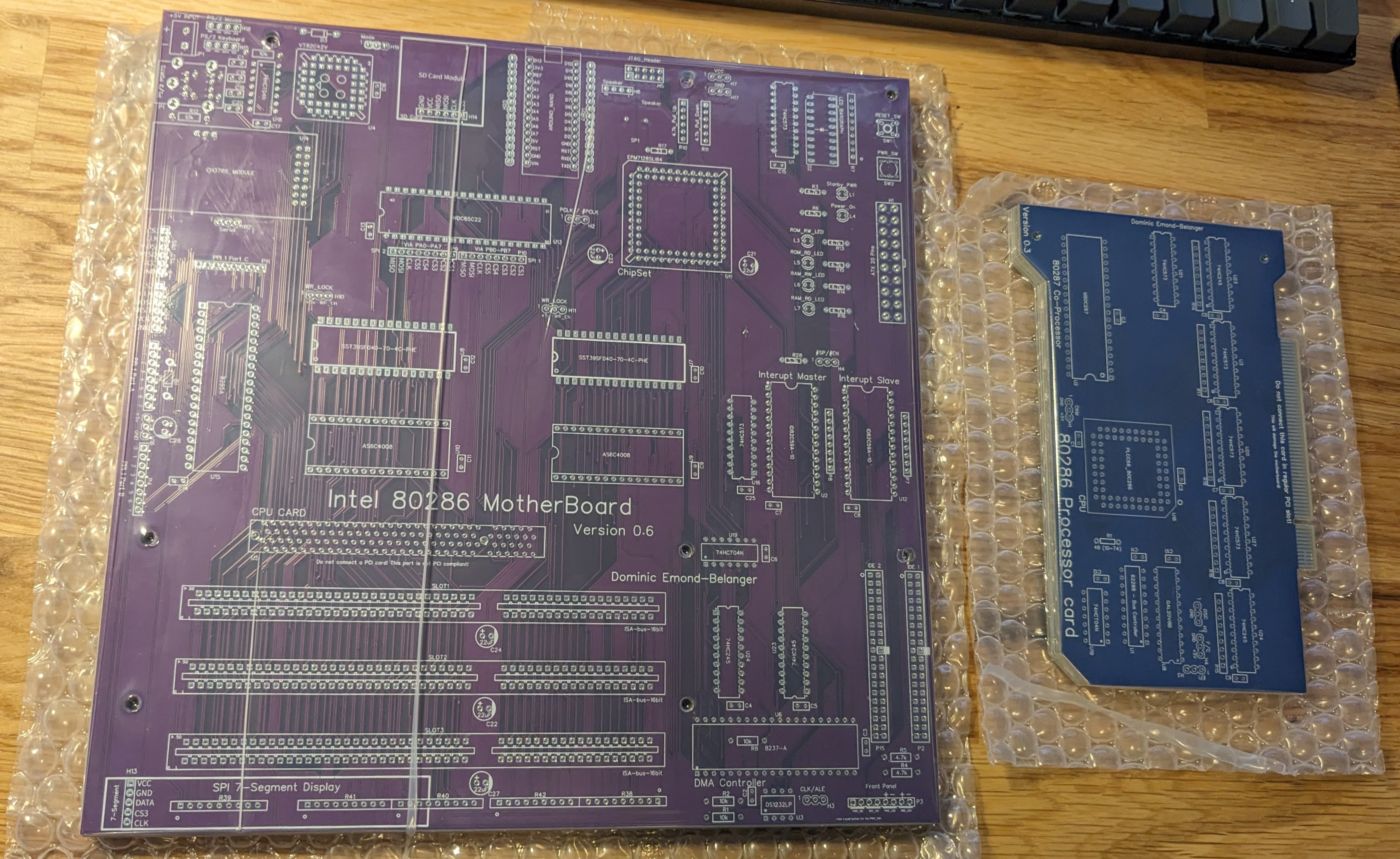
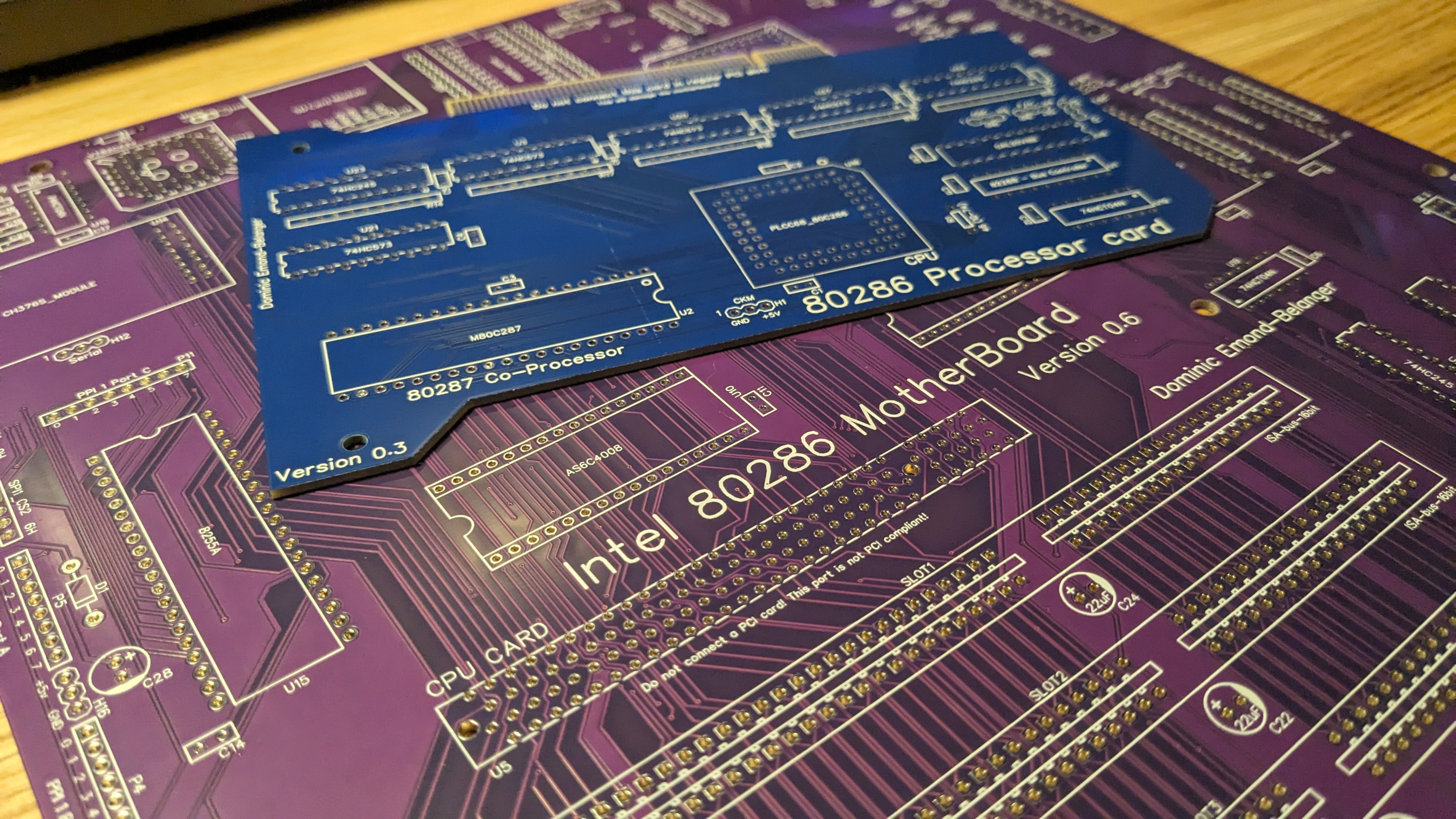
Motherboard v0.6 & CPU Card recieved
11/07/2023 at 23:58 • 0 comments![]()
Thanks for PCBWay for sponsoring the new PCBs production!
Just a quick post about the new boards revision that I recieved today from PCBWay. The process was very fast, placing order up to receiving the produced boards only took 5 buisness days total!
![]()
The boards were realy well packaged ![]()
After removing the board from their packaging, I’m realy happy about the finish and quality of the product.
![]()
The next step will be to start populating the sockets and test if the processor card is working correctly then I will be able to move to the motherboard.
-
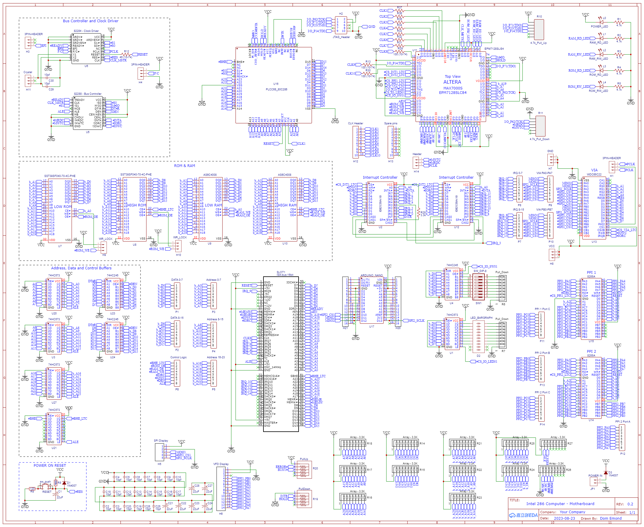
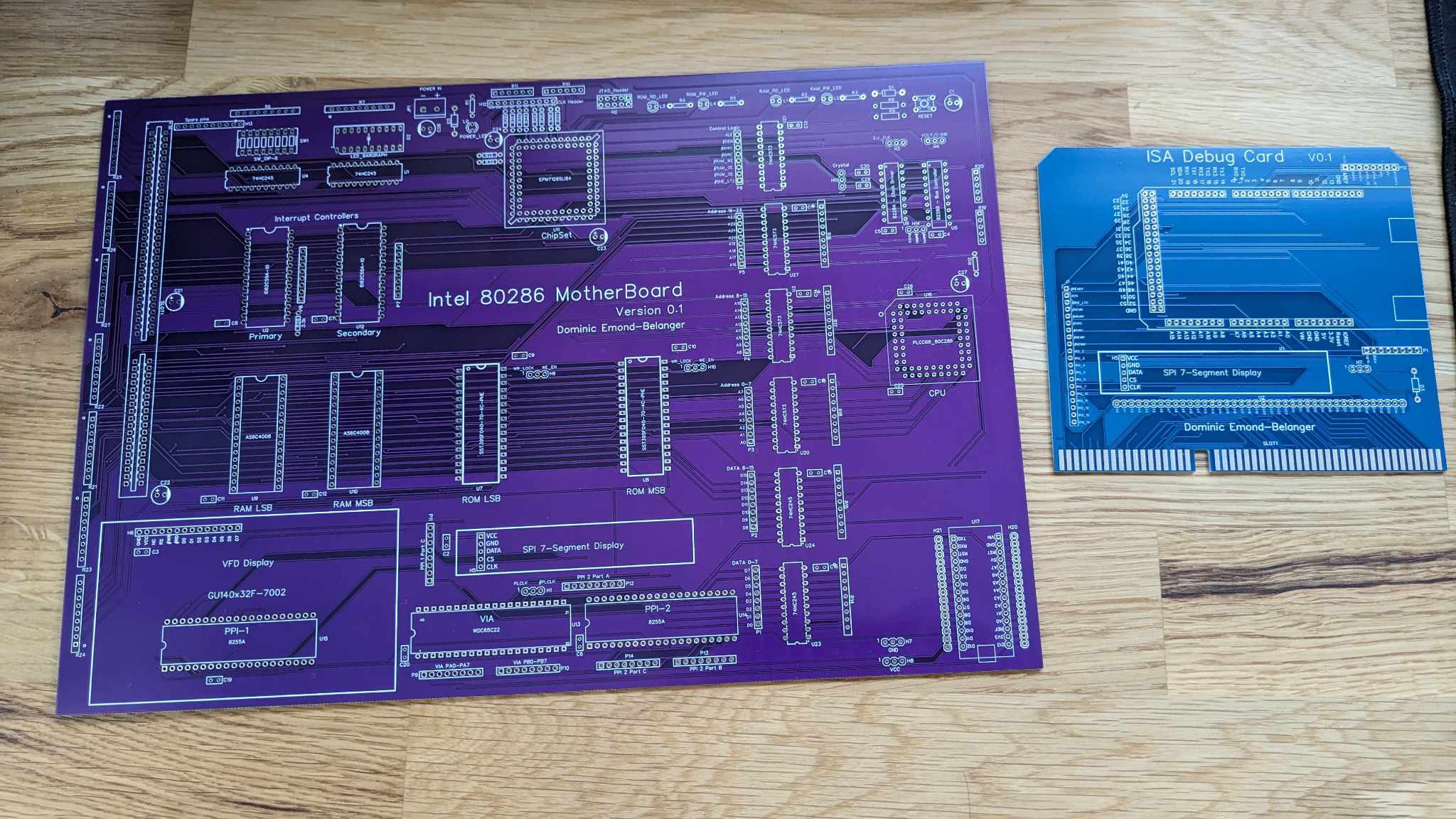
Motherboard v0.6 - Sponsor by PCBWay
11/01/2023 at 22:21 • 0 comments![]()
Thanks for PCBWay for sponsoring the new PCBs production, more on them later in this post!
I have been working on a new motherboard revision since early October 2023 to fix the issue I found in my first motherboard prototype and add some new features.
The new onboard features are :
- mATX form factor.
- ATX 20 pins power input.
- Front panel header with onboard power switch + reset.
- A PS/2 mouse and keyboard controller (VIA - VT82C42V).
- DMA Controller.
- Dual onboard IDE ports.
- Onboard PC speaker/buzzer + header.
- CH376S module footprint for USB stick support.
- SDCard Module via SPI.
Here's a preview of the new motherboard v0.6 :
![]()
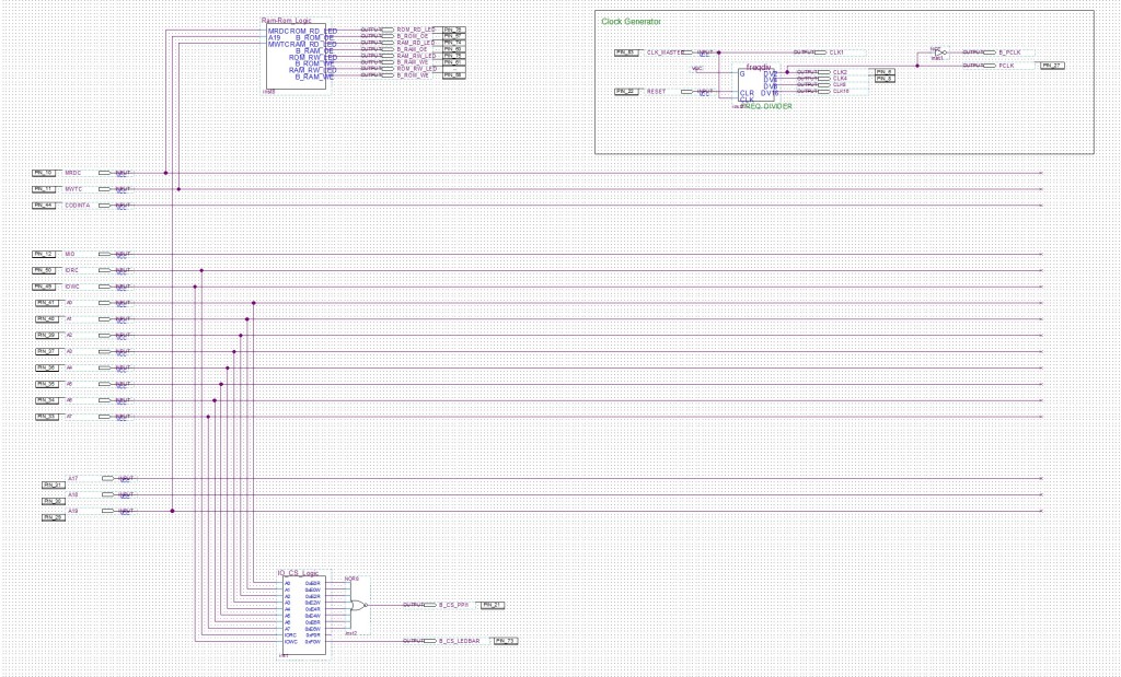
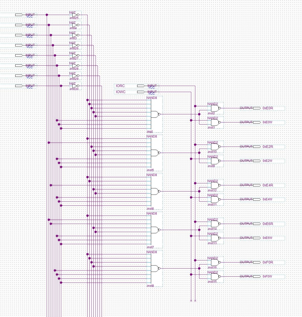
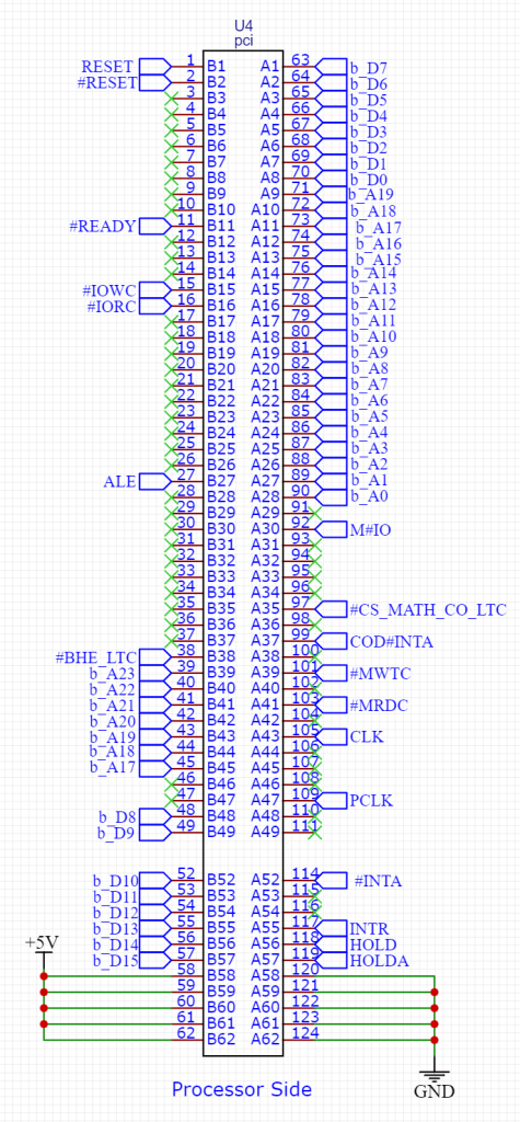
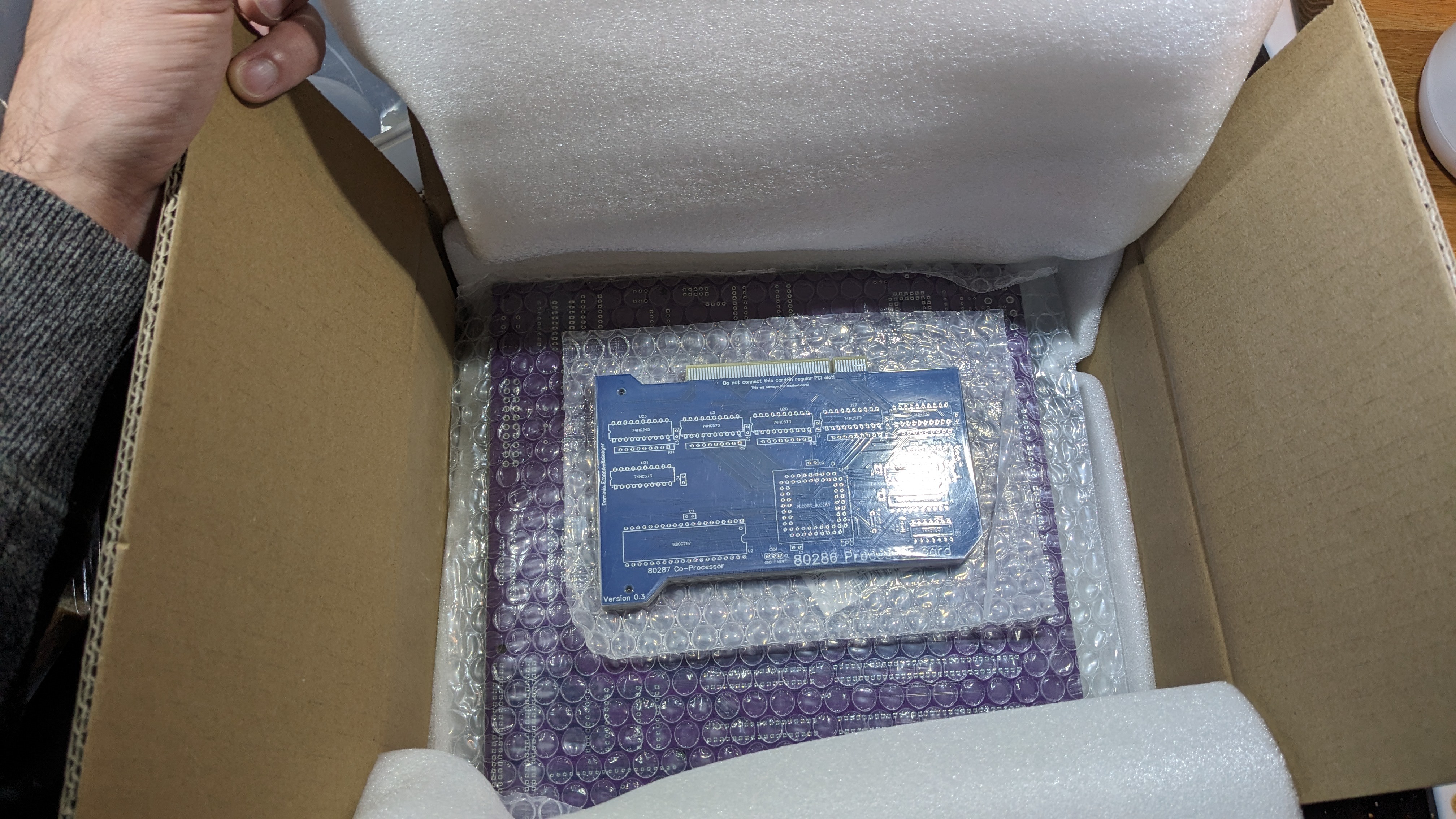
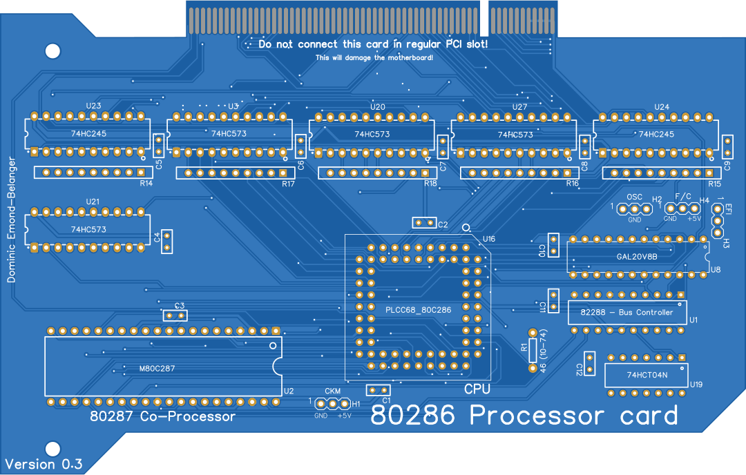
To be able to cramp everything on a 2 layers PCB with an mATX form factor, I had to make a imoprtant modification to the design. If you are looking at the expension slots, you can see that the first slot is labeled "CPU Card". Yes, the processor has been move onto a modular card with a PCI connector but beware, this port is not electricaly compatible with a standard PCI card!
![]()
This modification gave me the oportunity to move a good amount of ICs off the motherboard. All the bus transcievers has been moved to this card alongsdie the 82288 bus controller add a GAL20v8B acting as a clock generator chip. This gave me also the space to add a socket for a 80c287 Co-Processor!
The new motherboard v0.6 and the 80286 Processor card v0.3 where send to PCBWay to be produce this week. With their 3 to 4 days production time I should be able to do a review of the boards soon!
Thanks again to PCBWay for their great customer service!
-
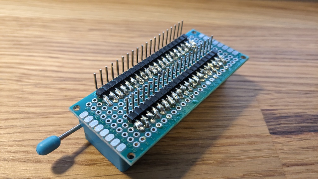
ZIF socketed ROM and future plans
10/21/2023 at 19:05 • 0 commentsTrying to upgrade the ROM sockets
I began to had connextions issue with my ROM sockets lately, this issue seem to be cause by the fact that I have to pull out the ROM chip all the time for programming and that cause the sockets to become loose with time. I ordered a pair of 32 pins ZIF sockets but after recieving it I realized that the board hole where not big enough for the ZIF socket pins..
My solution was the enlarge the hole with a small metal pic I had, at first everyhing seem to have worked great :
![]()
Mistakes where made..
But after testing, I realized that some address and data lines where not working anymore. After doing some contuinity test with my multimeter I concluded that I had broken some pads connection. After two days trying to fix my mistake I was still having random issues.
![]()
Bite the bullet
So I decided the bite the bullet and rebuild a new board from my spare PCB I had. I need to make sure that I remember all traces that need to be cut and to connect all the bodge wire from the “old” board. In the meanwile I soldered some headers instead of the ROM sockets and I constructed two little boards with 40 pins ZIF sockets then put a pair of 90 degres pins on the botom to be able the stack them on top of the header. That way theses ZIF board can be unplug and replace by normal sockets when no longer neede and they can be use on any 40 pins DIP chip in future projects :
![]()
Here’s a close-up shot off the botom of the ZIF boards, the 90 degres pins has been soldered like if there where SMD components. This gave them a little offset on the right or left of the original socket thus giving some clearance for some board design where ZIF sockets where not planned to be use :
![]()
Everything seem to be fitting well with the headers on the “new” motherboard :
![]()
The nexts steps are to reproduce all the modifications that I made on the last motherboard and begin the testing, after that I will be able to continue where I was before broking the last board.
Future plans
I had started to work on the next motherboard revision to fix the issues with the current version and add more flexibility. Here’s where I’m going for :
- The first thing I decided to do is to have a MATX form factor to be able to put my computer in a case.
- Put the CPU, the CO-Processor and lines transcievers on a daughter card.
- Replace the 80284 Clock Driver chip by a GAL20v8b.
- Adding a ATX power supply connector and front case panel header for power and reset switches.
- Onboard IDE support to be able to use a compact flash.
- Header spot to add a CH376S module for USB drive support.
- VT82C42V PS/2 keyboard controller.
- DS1232 chip to control power on reset and watchdog reset in case of crash.
- More SPI devices like a Real Time Clock, SD Card, 7-segments display and mabey a small EEPROM to save some settings.
- DMA controller socket for the future.
-
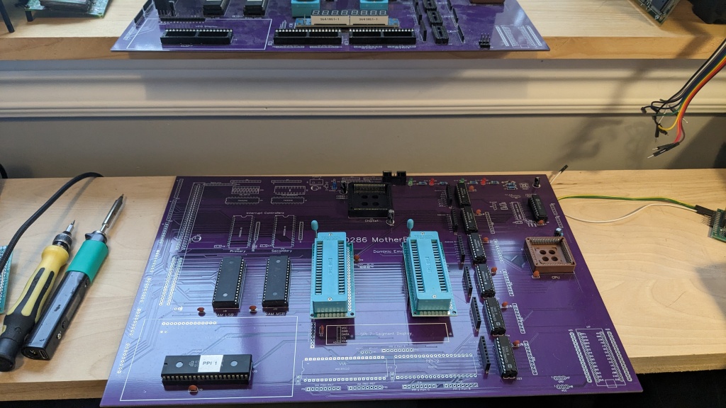
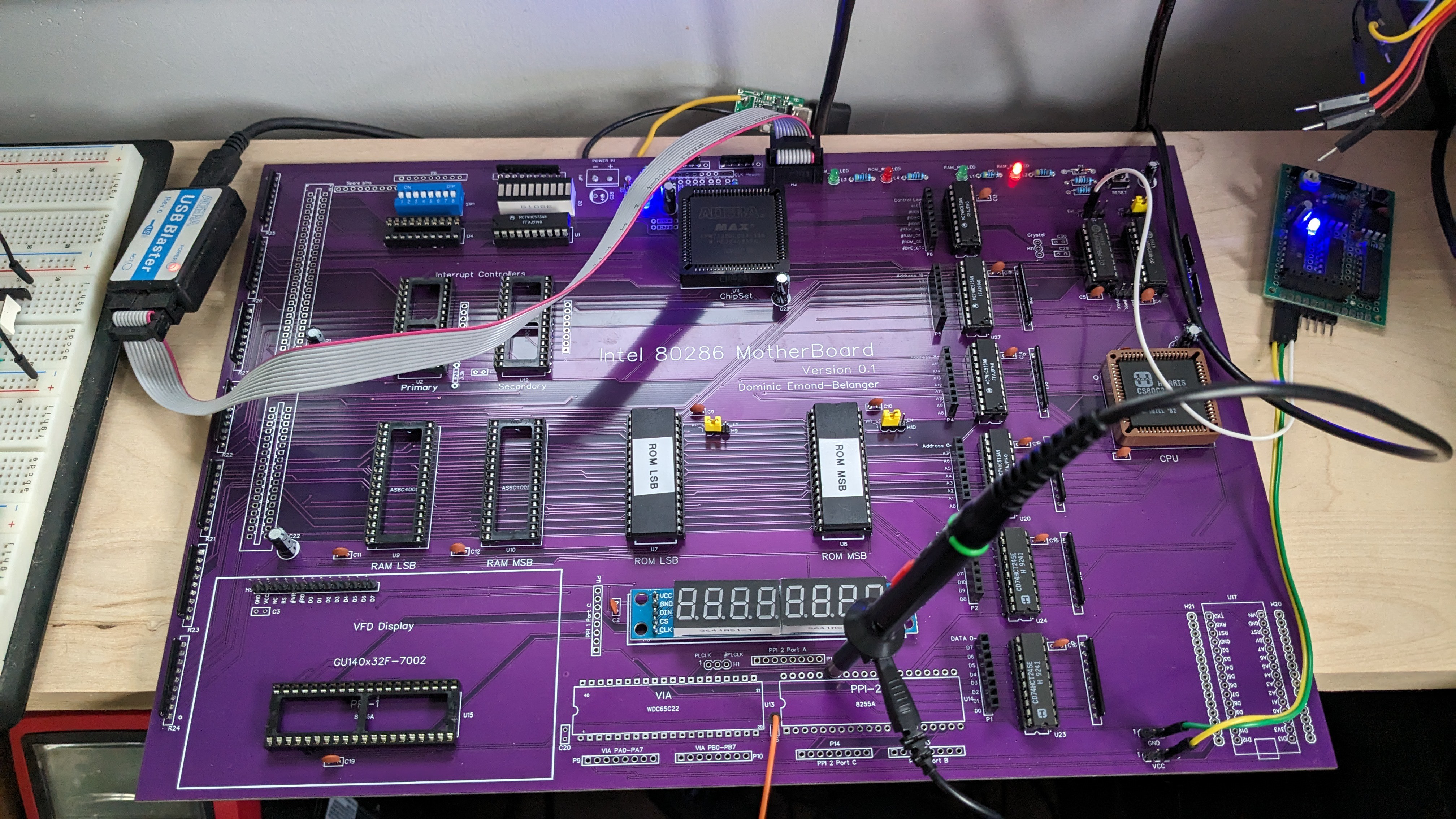
First motherboard prototype
10/15/2023 at 17:23 • 0 commentsHello, It's time for an update on my 80286 project!
I began to work on my 1st motherboard PCB prototype in the past month since working on a breadboard is becoming too challenging.
![]()
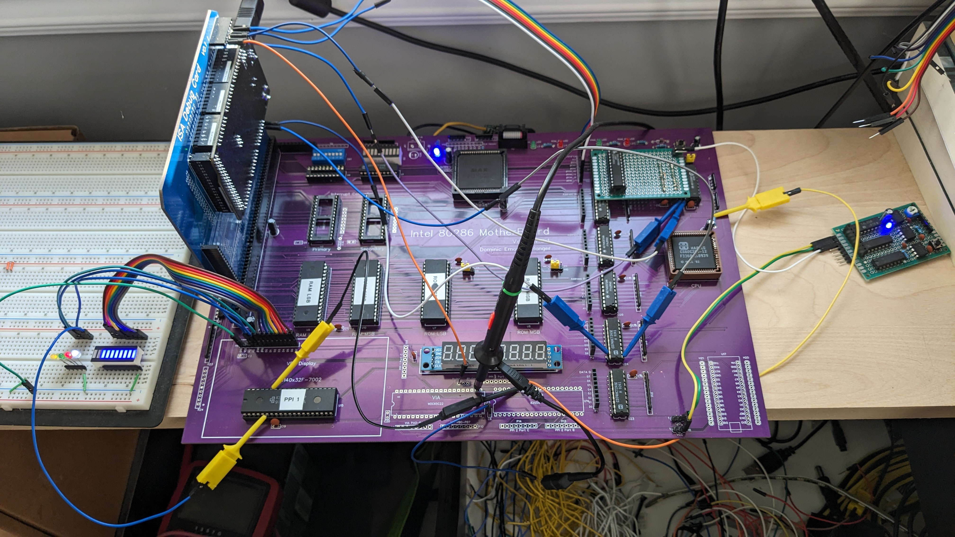
The goal of this version is to consolidate everything that is working on my breadboard version to a cleaner setup but let me add new things on top. I had also added a ISA port to plug a ISA debug card with the Arduino Mega for debuging.
Here's the final result after receiving the produced boards :
![]()
The first test run :
![]()
When testing the board I accidentally burned my 82C284 Clock Driver chip, luckily I was able to make a replacement with a GAL chip on a little protoboard.
And here's the first run I did with the debug card installed to troubleshoot the PPI :
![]()
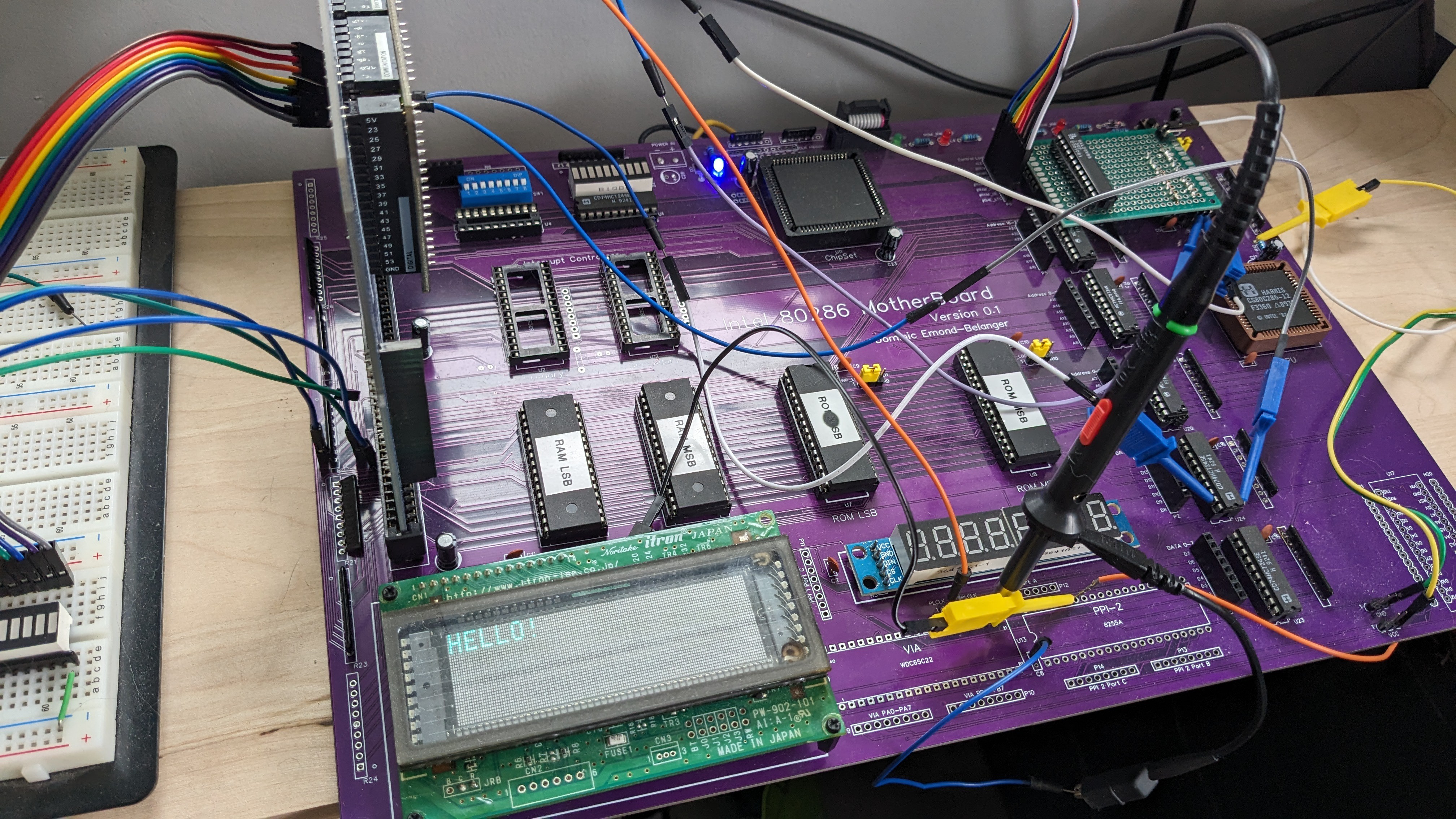
Finally after a week of troubleshooting, a lot of cut traces and bodge wires, I was able to make my VFD screen work again thru the PPI :
![]()
The next step will be to use this platform to learn more about x86 assembly and begin work on a BIOS.
Until next time...
Dom
-
Starting to work on a 80286 system - First 6 months (mega dump)
08/25/2023 at 13:10 • 0 commentsAt the time of writing this line I'm 8 month in the project so I'll try to start from the beginning and explain everything that I did since the begining as a recap.
Sorry in advance for my questionable english, it's not my first language.
Febuary 2023
After a year without working on a retro project I decided to start a new project with a intel 80286 that I had found in a parts bin at my workplace. First thing was to read on the subject then I had come across rehsd 80286 project on Youtube (Playlist here) that inspired me to realy start working on it.
Here's the ressources that I had read up to this point :
- Harris 80c286 Datasheet
- Intel 80286 Programmer's Reference Manual
- rehsd - 80286 Build : Youtube playlist and website
- Saldor - 16-bit Intel x86 breadboard computer : Youtube playlist
March to May 2023
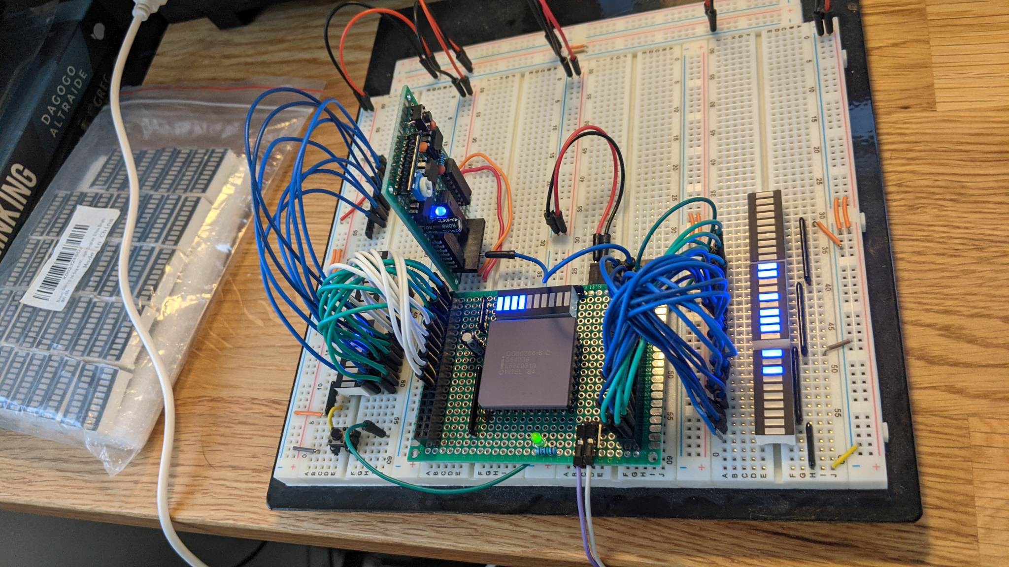
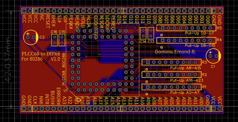
My wife and I got our first baby in March so I did not worked much on my retro projects during 2-3 months. Nontheless I had the time to work on my first breakout board for my 80286 CPU and learn how to control the CPU.
I builded a clock circuit with a 555 timer and a variable resistor to help me debug the CPU (the vertical board on the photo).
![]()
At that point I began to realize that I needed to order some ICs to help me generate some control signals for the CPU. So I ordered the following ICs :
- 80284 - Clock driver
- 80288 - Bus Controller
- 74HCT245 - for the Data Bus transcivers
- 74HCT573 - for the Address Bus transcivers
June 2023
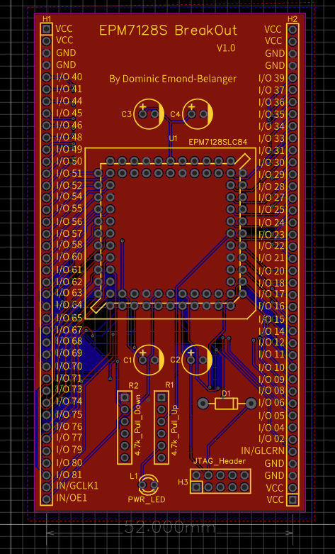
In my last Z80 I ordered some Altera Max CPLD but after thinkering for a wihile I realized that I had no idea how to program or use them so I put them away. Now I think is time to give them another chance to help me with the glue logic for my 80286. After reading around, I'd put togheter a CPLD programmer on a protoboard for my Altera Max and bought a USB Blaster to connect and program the CPLD via the JTAG header at the botom-right of the board :
![]()
After a week of debuging the connections and learning the Quartus software, I was able to upload my first logic to the CPLD.
Now I that I had a working CPU and CPLD breakout boards, I decided to produce some PCBs to cleanly build on a Breadboard :
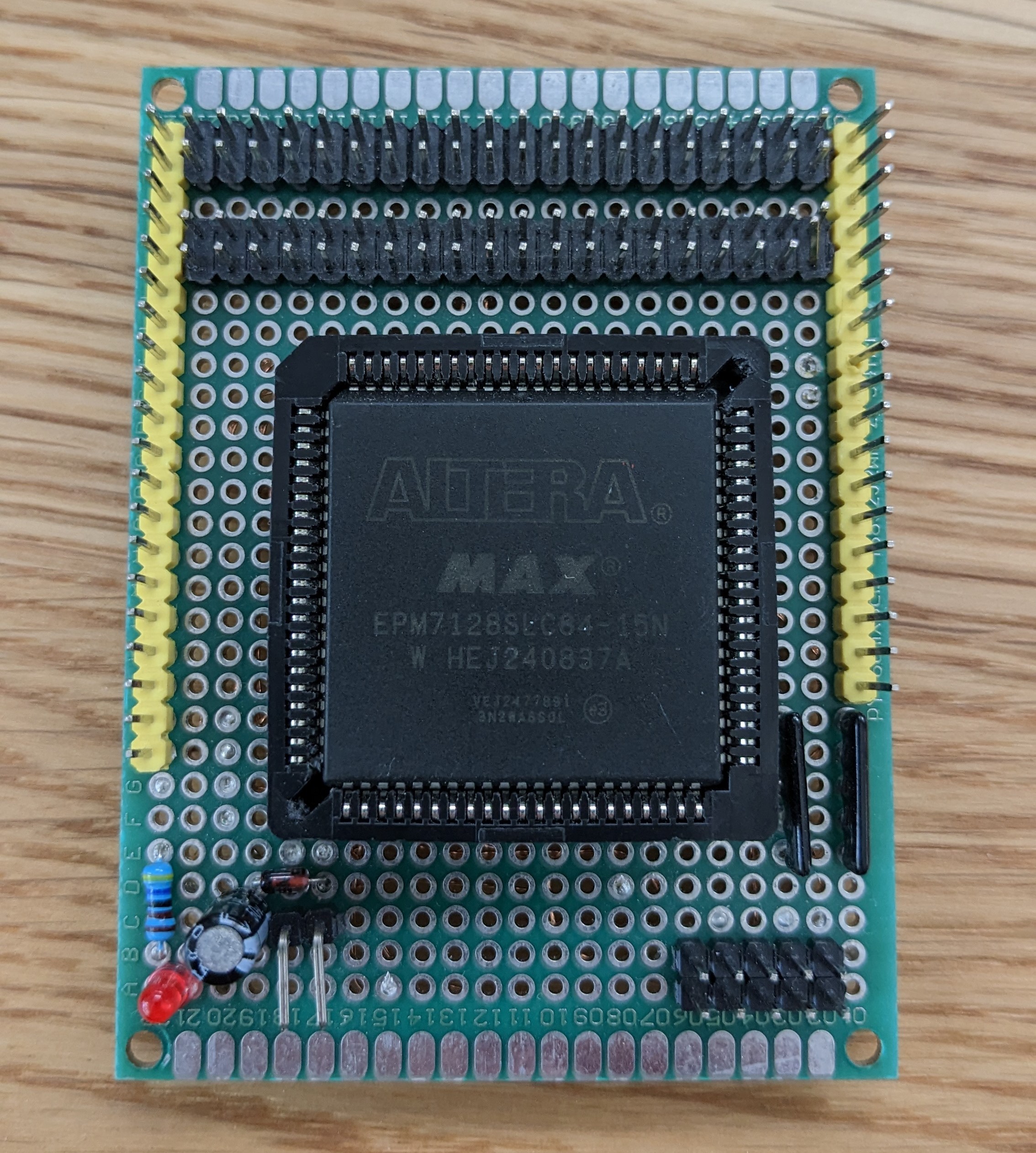
80286 CPU Breakout board :
![]()
CPLD Breakout board :
![]()
July 2023
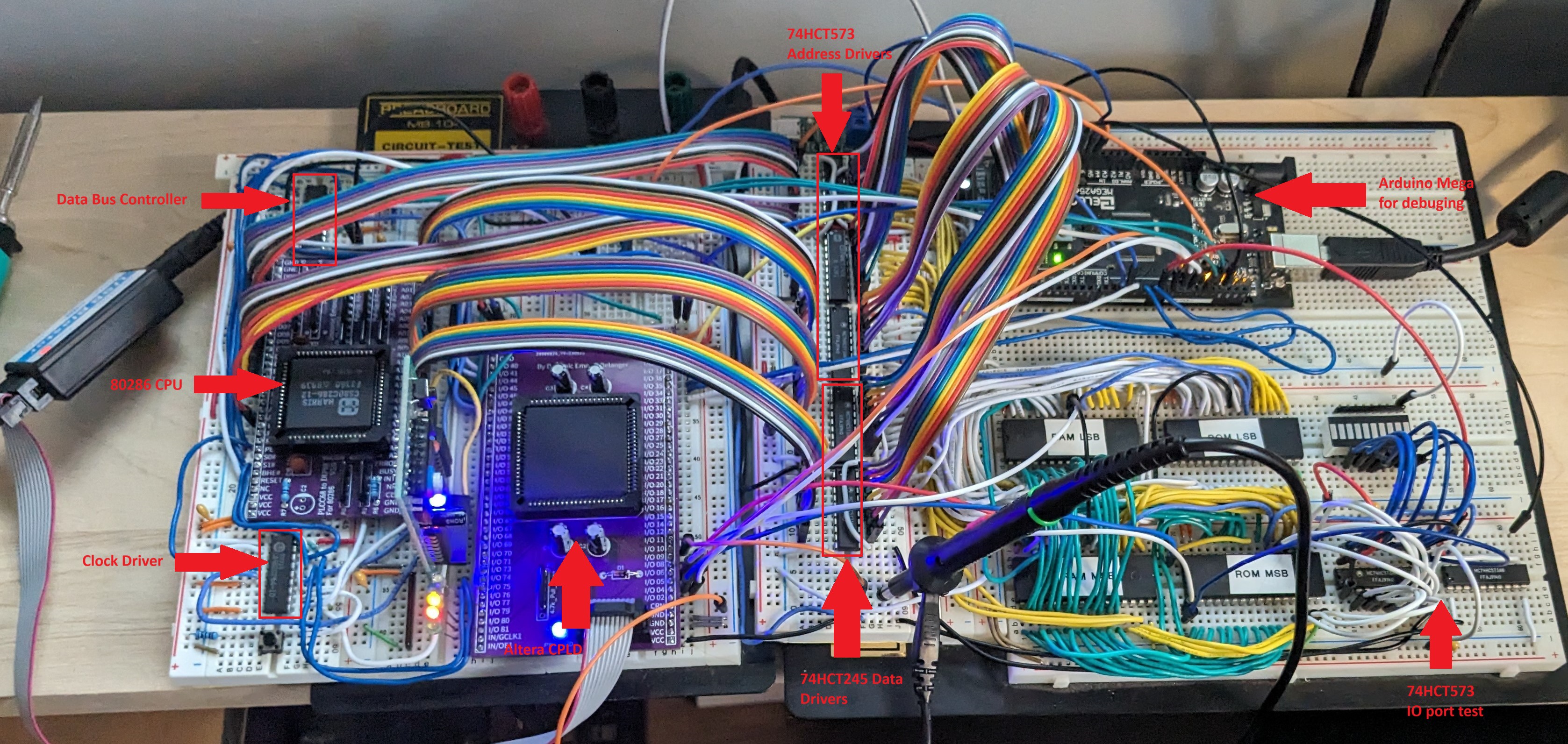
As soon I recived my new boards, I began to build a simple prototype version of my computer with some RAM, ROM and I/O port to test some basic code. I used an Arduino Mega to debug the address and data line (based on rehsd design) :
![]()
After 3 weeks of debuging I was able to make some basic code that output value to the LED bargraph located on the right of the breadboard. Next step was to interface with something more complex, I had some VFD screens with a 8 bits parallel interface in my parts bin so I decided to gave it a shot.
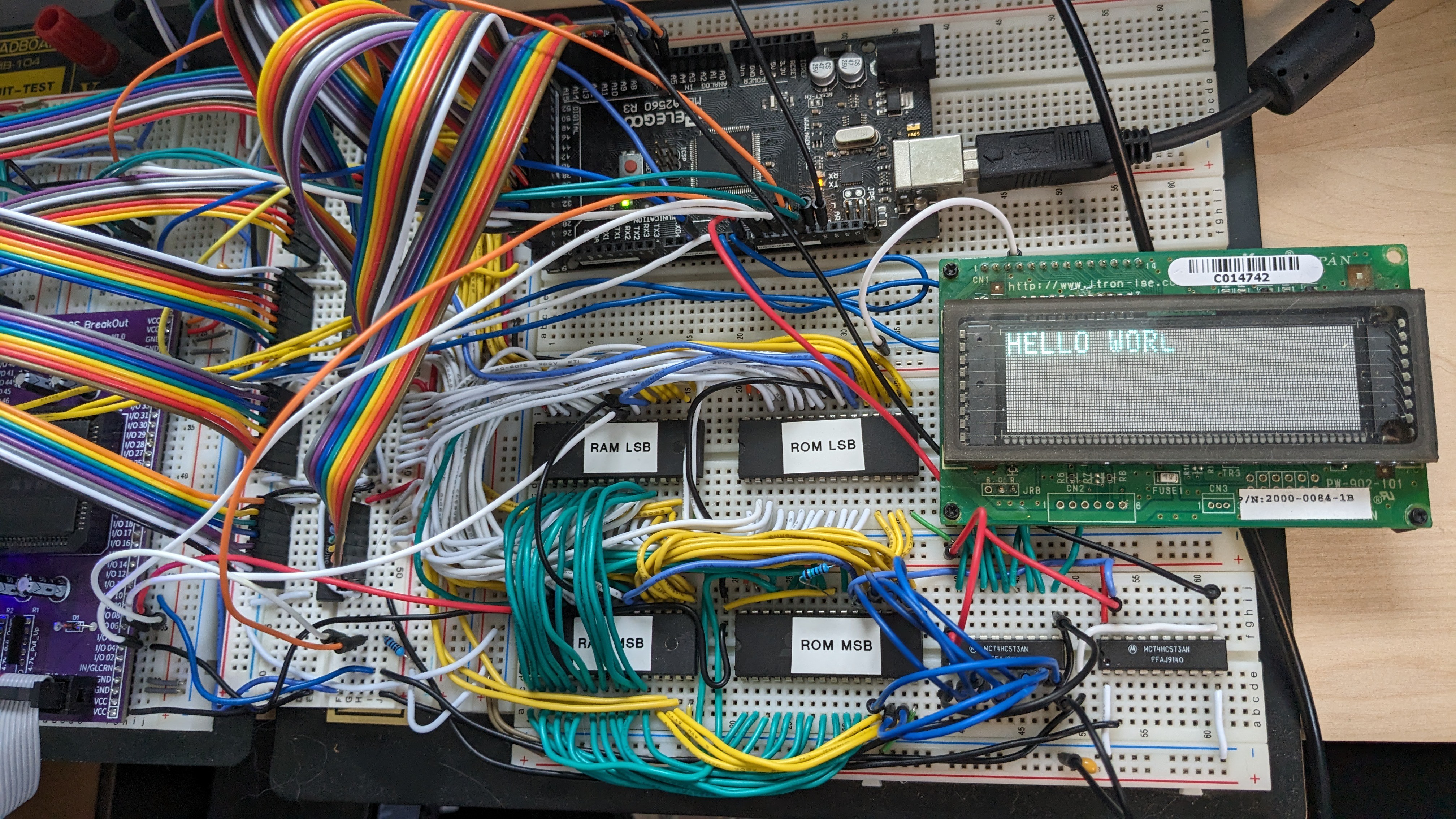
![]()
I was able to output the classic 'Hello World' on the VFD screen. (The last letters are not seen due to the camera shutter)
Now that I'm able to write to the I/O port I decided to order more chips for more complex interactions :
- W65C22 - Western Digital - Versatile Interface Adapter (VIA)
- KS82C55A - Samsung - Programmable Peripheral Adapter (PPI)
When Ebay shoping for the VIA and PPI chips I stumble on a broken Tandon 80286 motherboard sold only for parts, so I decided to grab it and try to reverse engineer the board to gain some insight on its design.
To be continued ...
Dom
Intel 80286 HomeBrew Computer
A HomeBrew Intel 80286 computer with ISA ports