Tom
Tom-
2023 End Of Year Update
01/01/2024 at 01:37 • 0 commentsIt has been a while since I last provided an update, and there have been a number of developments and interesting things in that time!
Revision 2 CPU Board
Following my previous update where I had identified several changes that were due for revision 2 of COMET68k. In November I ordered the PCBs with high hopes for resolving a number of issues outstanding from revision 1.
To address these points:
- Having added pull-up/down resistors in strategic places, the board now starts much more reliably with the expansion bus buffers in place. I do still seem to be experiencing a bit of instability on power up that I am still investigating, however. It usually requires me to power cycle a couple more times before it will start to work. I have a theory that I am investigating, and hopefully it will be a relatively simple change to the CPLD to fix...
- Having tested the new power-on reset and watchdog timeout flag logic on a breadboard, these flags now accurately reflect what happened after a reset.
- The signal that I routed to the CPLD last minute, and which caused the short between the internal layers is fixed, and has now been permanently assigned as a means of generating a software IRQ to the CPU. With some other changes I made (which slightly modify the memory map from revision 1) I have added an ability to read the link status of the Ethernet controller, and still managed to maintain one signal routed to the CPLD that I can toggle which maybe I can use for something in the future (although I still have no idea what that might be at this moment in time.)
There were some minor issues during construction, namely some pins which did not reflow on some parts. This is probably an issue with my placement technique and maybe the fact that I use a lot of "new old stock" parts that may not have necessarily been stored correctly over time and whos pins are less receptive of solder. Most of the issues were on the Ethernet controller, with a few pins also requiring some touch up on the CPLD, and one pin on the CPU. Technique wise, I probably need to press the components down into the solder paste rather than simply sitting them on top of it...
As of writing I have identified a few more things which could constitute a 3rd revision, however, I do not currently know whether I will actually build a 3rd revision or move on to a more capable (e.g. 68030 based) system.
![]()
Revision 2 fully assembled FreeRTOS+TCP
An early goal of COMET68k was to port FreeRTOS and its TCP/IP stack to my board, and I've managed to achieve this goal. For TCP/IP performance, in my testing I was able to achieve upwards of 200pps or about a megabit of throughput when running a ping flood with various packet sizes. I feel like that is quite reasonable for a 10MHz processor doing almost everything in software (the only "hardware acceleration" being packet transmission and reception handled through DMA by the Ethernet controller).
At the moment I maintain my own copy of the FreeRTOS kernel including my port on github, but I plan to publish this to a repository managed by FreeRTOS themselves which contains community maintained ports. I feel this will be a much better place for this port to be housed, so keep an eye on that for my latest port (which is much enhanced over the port I currently have published). Whether the FreeRTOS+TCP port can also be maintained here is something that I need to determine.
CP/M-68k
While my original (stretch) goal was to get something like uClinux running on my board, this feels a bit beyond my capabilities for the time being.
So instead, over the christmas break, I put some effort in to making CP/M-68k work, and I have written a BIOS to work with my hardware. Although it is a somewhat simplistic OS (compared with a modern MS-DOS for example), it at least provides something for me to work with and test out some of the expansion hardware that I have built, and will provide a platform for testing additional hardware (and software!) in the future.
It is also possible to get hold of the source code for CP/M-68k, and the downloads also contain assemblers, compilers and linkers, so it should even be possible to modify/extend CP/M and write new software for it. The supplied editor is simplistic (a lot like edlin for DOS), and I haven't fully worked out how to use it, but I think a means to get files on and off using something like Xmodem or similar would be the way to go, then I can write code with a more capable editor.
Getting CP/M running was an interesting task in itself, and was not immediately obvious to me about how to actually do it (although I did later clock on to something in the documentation that made it all fall in to place, only after I had picked the brains of a friend who has already done it and gave me some pointers). I'll add a post detailing this process to my list for the future as it may help someone else who is looking to tackle this as well.
I don't know if I'll release the source code for this BIOS, it is a bit thrown together. I need to sit down and re-write it, and modularise it better to make it extendable and easier to maintain.
Expansion Bus
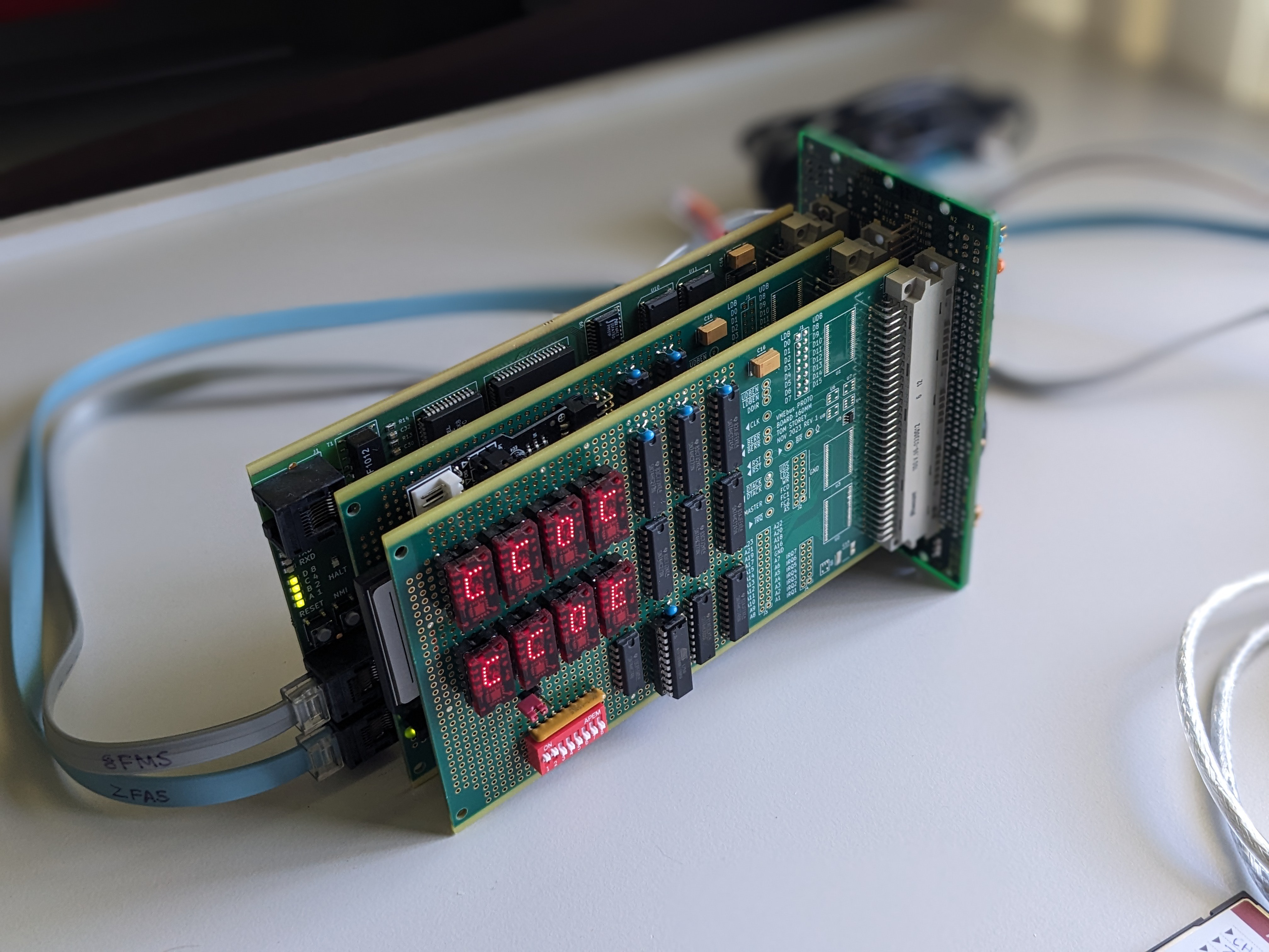
The expansion bus is now fully operational, and for the first time, COMET68k was able to drive something else other than its own on-board peripherals! I built a couple of expansion boards to put the expansion bus through its paces, and so far the results are positive. There is still more work to be done in this area, such as testing interrupts and bus mastership from external sources.
Expansion Modules
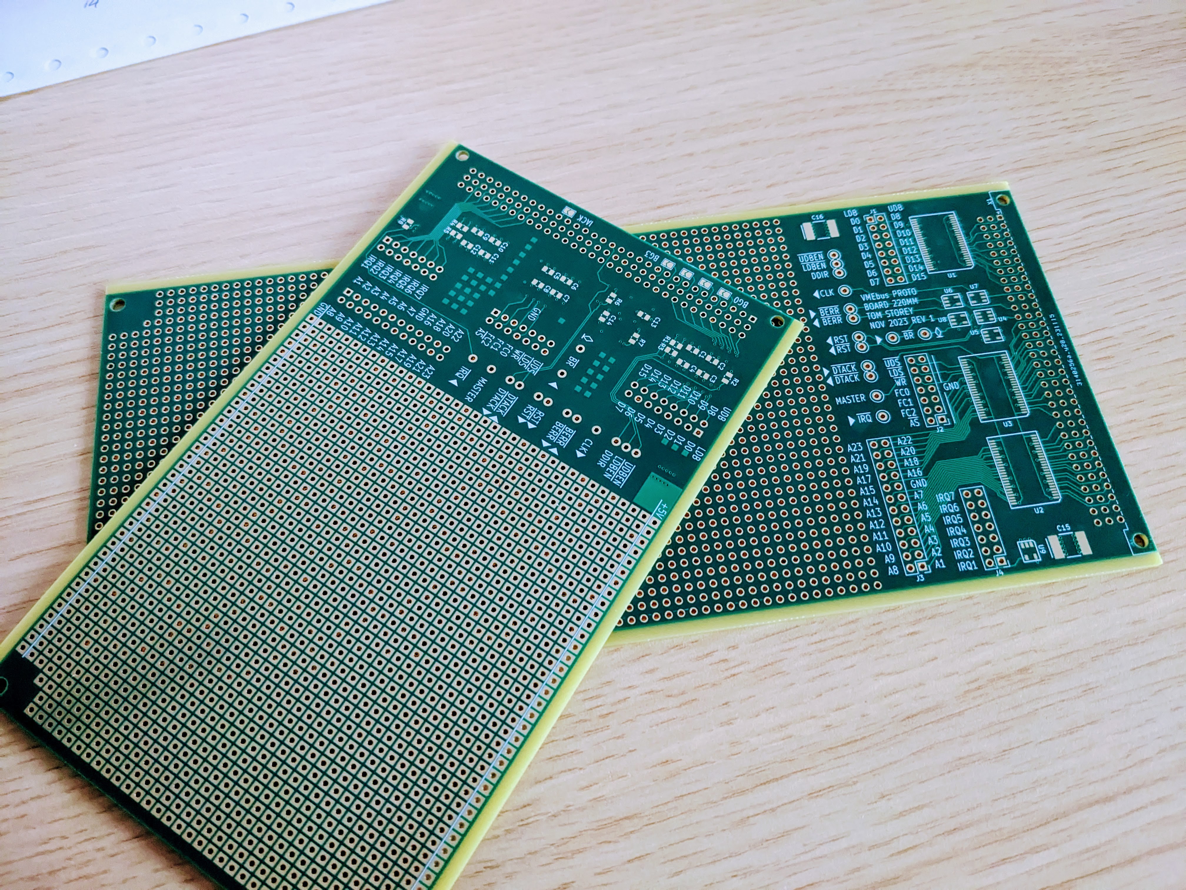
WIth revision 2 having its expansion bus functional it became necessary to build some hardware to test it out. This involved designing two VMEbus prototyping boards with some pre-staged components and signal breakouts to remove some of the tedium of the initial buildout of each board, but with (hopefully) enough flexibility to allow me to build a good array of modules that act as both bus masters and slaves.
The pre-staging area took up quite a bit of the board area, so I decided to build two different sizes of prototyping boards, 100x160mm and 100x220mm. These are both standard Eurocard sizes, and although the 100x220mm boards will be useful for prototyping larger more complex designs, ideally I'll avoid building anything on boards that size and concentrate on 100x160mm boards so that they all fit nicely within my subrack.
![]()
VMEbus prototyping boards ![]()
My idea of "full stack development" To that end, two boards have been built to date...
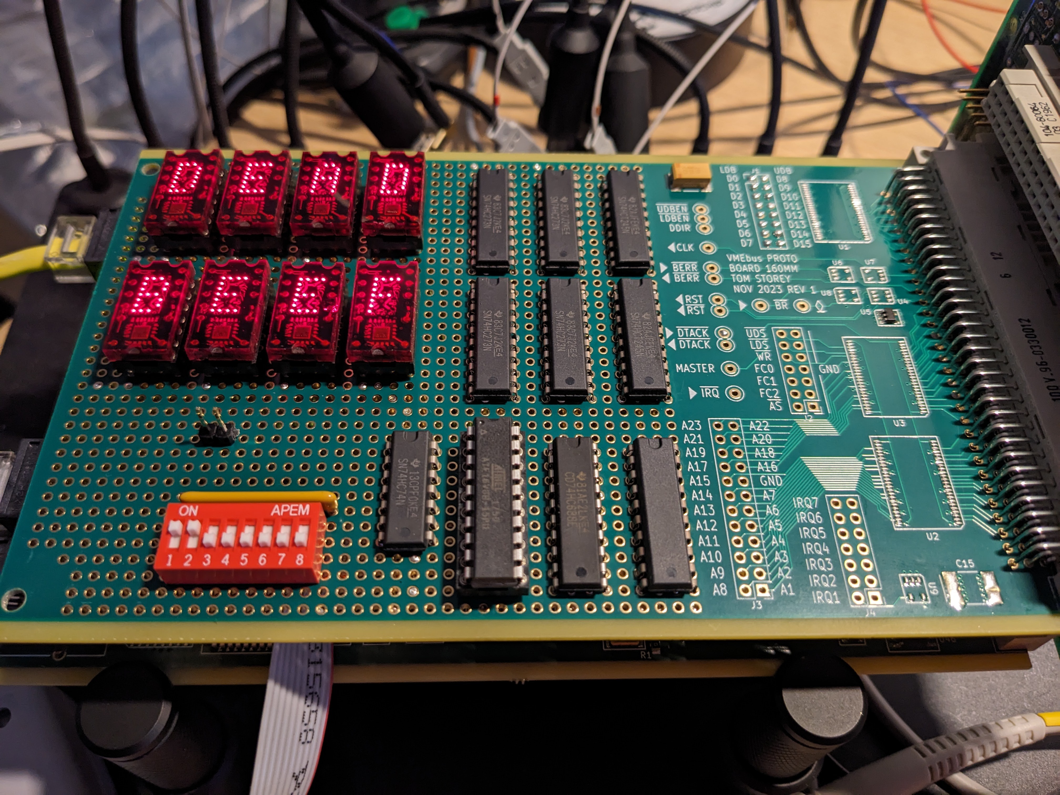
Debug display board
The first board I built was a simple "debug" display board, or perhaps something of a POST analyser card.
It has two sets of four TIL311/DIS1417 style displays that allow writing of either one long value (32 bits), or two individual word values (16 bits). Each word write shifts the value from one set of displays to the next, providing either a single display of one long value, or a short history of two word values.
I also implemented a function which just serves to disable the displays, allowing you to "clear" them prior to starting a new debug session, or if you perhaps only want to display a single word value. This is accessed simply by "reading" the displays, although no useful value is returned by that read.
This board came in handy while developing my CP/M BIOS because it allowed me to track progress of the code and see where things were getting stuck or crashing (or to discover new BIOS functions that I needed to implement).
![]()
![]()
Compact Flash/IDE board
The second board that I built provides an IDE style interface to allow me to access a compact flash card. Testing a variety of CF cards has so far been successful, however, with COMET68k only running at 10MHz it may be hiding some issues which are yet to rear their heads. A friend who has built a 68030 based system that is running at speeds up to 33MHz has reported a lot of success with many different CF cards except for one, so that does at least provide some confidence.
My CP/M BIOS is able to interact with the CF board to read and write disk sectors, and read/write/verify tests using the "PIP" utility to copy the contents of one disk to another have so far been very positive with no failures over several hours.
I have designs underway for another version that will have a CF socket directly on the board allowing me access to a couple of other interesting signals that aren't provided by the IDE interface, such as card presence, and the IORDY signal which I believe I can tie in to the DTACK logic and which may help to better support slower cards in faster systems.
![]()
![]()
If you happen to be wondering why I haven't used the pre-staged component positions on the above two boards, it comes down to logic families and voltage thresholds. Most of the parts I have in stock are HC family, which generally require something close to 5V to consider a signal as logic high. A VMEbus backplane floats most signals at around 2.9V due to the termination resistors, and this falls within the non-linear region of a CMOS input. I need to stock up on more HCT family parts and then I can interface more directly with the pre-staged buffer positions (which in my case use FCT family parts).
git Repository
In my previous post I mentioned that I was working on preparing my git repository for public consumption, and this is still a work in progress. I guess my feeling at the moment is that I have a lot of in-flight designs that I would like to try and get to a better state of completion before I release them to the public.
I'll keep working to make this available, as I have had expressions of interest from some people to be able to see my design files, and I am keen to share them.
Please stay tuned! :-)
-
COMET68k System Architecture
09/19/2023 at 11:02 • 0 commentsIn this post I want to go over the architecture of COMET68k in some more detail. Specifically I'll describe the busses that exist, which peripherals are on them, and how they function.
Basic Architecture
COMET68k is an enhanced collection of peripherals integrated onto one PCB, enough to make a rather capable standalone or single board computer (if all you care about is serial for input/output). These peripherals are connected to two basic busses, with a 3rd bus providing expansion capability:
- The processor "local" bus contains all 16-bit capable peripherals and devices
- The peripheral "X" bus contains all 8-bit peripherals
- The expansion "system" bus is a buffered copy of the local bus
All of the above busses relate to the data portion of the bus. The address bus is largely singular, except when it comes to the expansion header where most signals are buffered in some way. One address signal is synthesised from the upper data strobe to produce XA0 for the X bus to permit 8-bit devices to be readable and writeable on sequential addresses.
Here is a diagram showing how all of the peripherals fit in to these busses:

Local Bus
The local bus is the bus which is directly connected to the CPU. Its a 16-bit wide bus connecting directly to DRAM, the ethernet controller, the X bus buffers and latches, and buffers for the system bus. The CPU and ethernet controller can both be bus masters, and therefore have direct 16-bit access to DRAM to read instructions and data. This is particularly important for the ethernet controller so that it can DMA packet data as quickly as possible to and from DRAM during transmit and receive operations.
I chose the Am79C90 ethernet controller specifically for its capability to work directly from memory (also known as "zero copy") as this removes the need to copy packets to and from FIFOs or RAM internal to the ethernet controller itself. Although it complicates the system design a little bit, it helps improve performance.
X Bus
I refer to this as the "cross" or "X" bus because it allows 8-bit peripheral data to be directed to or from either half of the CPU local bus. The X bus houses all 8-bit peripherals such as the RTC, UARTs, and some GPIO to allow control of some status LEDs, ethernet loopback options, and reading of configuraiton jumpers and other status bits. It also houses both of the ROM sockets that the CPU executes code from.
As I mentioned in my first post, I have implemented a technique which permits execution of code from a single 8-bit wide ROM, despite the CPU having a 16-bit interface. This is achieved using a latch and buffer which, when directed appropriately, can enable a 16-bit value to be read from the ROM and presented to the CPU. The idea is shamelessly borrowed from a HP JetDirect print server card that I bought in a rummage sale. But I want to give you a more detailed look at how it works, and I think an (annotated) timing diagram is probably the best way to do this with a bried explanation of a 68000 cycle (you can click the image to access the Wavedrom website and view the source of this diagram).

At the falling edge of CPU state S0 the CPU asserts an address on to the address bus (a), arming address decoding circuitry.
At the rising edge following S1 the CPU the CPU then asserts its Address Strobe signal to indicate that the address is valid (b). This then causes the ROM chip select signal to be asserted (c) and it starts outputting data for the lower byte of data.
At the next negative edge of the 40MHz clock the X bus state machine has started to assert some of the control signals required to interface the X bus to the CPU local bus, in this case allowing the contents of the X Data bus through to the lower half of the CPU local bus (d) via a latch. It then proceeds to implement a small delay to satisfy the access time of the ROM.
At the end of this delay several things happen at marker (e):
- The latch enable signal is brought high to stabilise the data on the lower half of the CPU local bus
- XA0 is brought low to begin accessing the upper half of the word that is being read from ROM
- The buffer between the X Data bus and the upper half of the CPU local bus is enabled
- DTACK/ is asserted to indicate to the CPU that it may end the cycle when it is ready
At this point the X bus state machine moves to a state where it waits for AS/ to be negated. At the falling edge of the CPU clock at the end of S4 the CPU will begin looking for DTACK/ to be asserted so that it can end its current cycle, which we have already done and thus this will begin to happen immediately. But the cycle doesnt end immediately, it takes one more CPU clock cycle worth of time for the cycle to end, providing sufficient time for the upper half of the word in the ROM to be presented and stabilise on the upper half of the CPU local bus.
At (f) the CPU is ending its bus cycle by negating AS/. This causes DTACK/ to be negated by the X bus state machine, along with the ROM chip select which stops outputting data. The X bus state machine recognises that AS/ has been negated at the next falling edge of the 40MHz clock, and will then reset all of its control signals to their initial state (g) and proceed back to its idle state to wait for another cycle.
And there we have it, a word has been read from a single 8-bit ROM and presented to the CPU on its 16-bit data bus without requiring any wait states. This scheme and its timing is heavily tied to and factored on the CPLD clock (40MHz) being 4x the CPU clock. At higher CPU speeds this required modification to adjust the point at which DTACK/ is asserted to ensure that all required timing is met and the CPU doesnt end up reading garbage from the ROM.
For those of you who are familiar with the 68k, you may have noticed that there is no mention of the UDS/ and LDS/ signals above. For simplicity sake, a read of any size from the ROM always causes a full word to be read and presented towards the CPU. This makes use of the behaviour of the CPU whereby it will take what ever data it needs from the appropriate halves of the data bus given the operation being performed. And since a word read fits within a single CPU cycle anyway, there is no advantage gained from handling byte reads.
System Bus
The system bus is the bus which permits the system to be expanded with external peripherals on additional cards. It mostly comprises of a buffered copy of the address and data busses from the CPU, along with many of the control signals. Physically it follows the VMEbus standard for its pinout, but logically it is more like a standard asynchronous expansion bus with multi-master capability to allow DMA operations.
It is a bi-directional bus, whereby an off-board master taking control of the bus causes all of the on-board peripherals and memories to be accessible externally. This would permit, for example, a second ethernet interface to be provided on another card, which would be able to send and receive packets from memory contained on the COMET68k board itself. This is the theory at least - at time of writing (and due to not having any expansion capability due to a design issue with my rev 1 board) this is the only functionality not yet tested in the design.
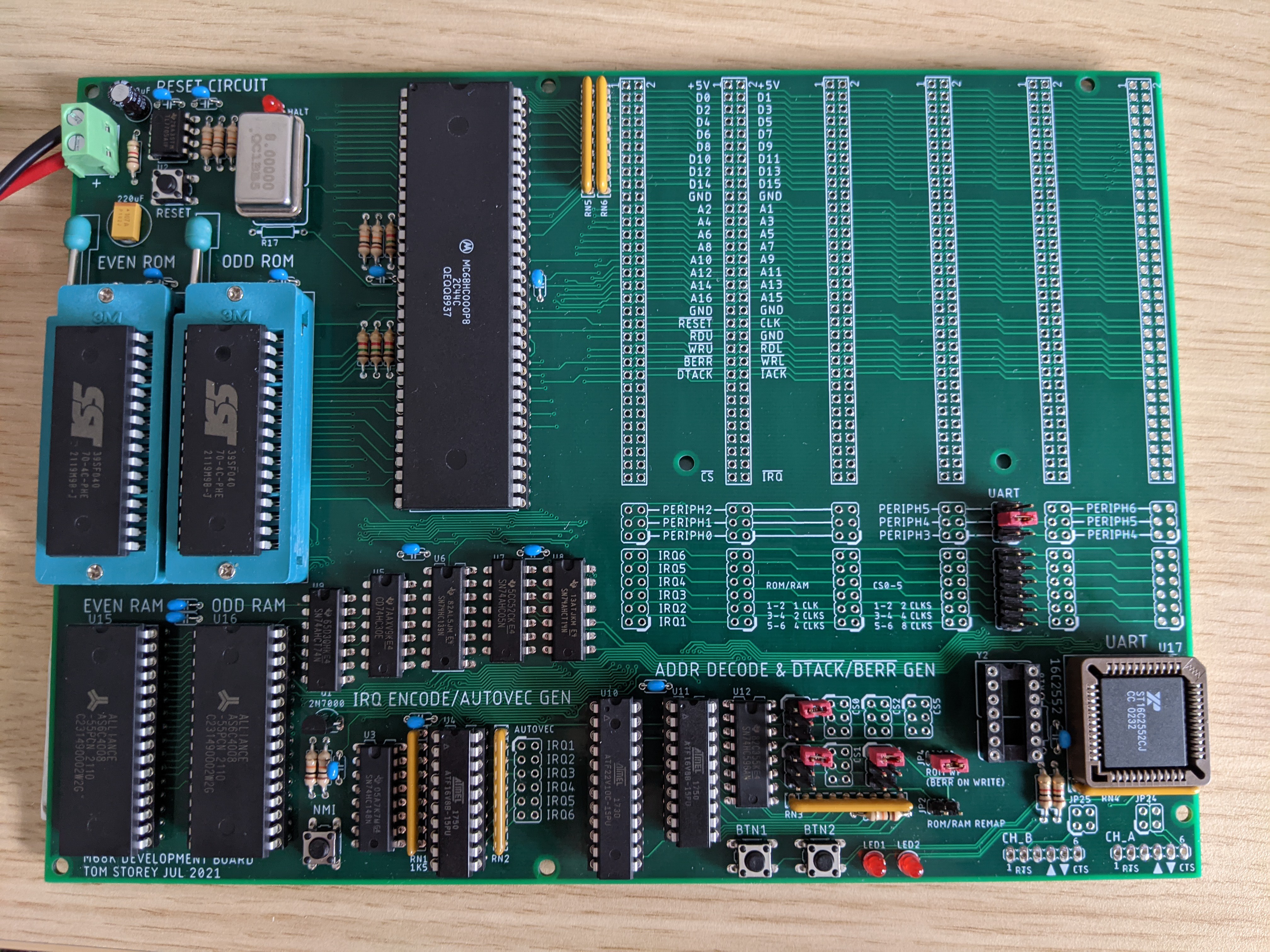
CPLD
The CPLD glues everything together and implements a lot of logic that might otherwise be done in discrete chips. For a board with this level of integration and in such a form factor, it would not be possible without using a CPLD (or a small FPGA) as the quantity of discrete logic required would far exceed the board space available.
The CPLD is responsible for many and varied tasks:
- Clock generation for the CPU, ethernet controller and timers
- DRAM refreshing
- Address decoding for various peripheral address ranges
- Bus watchdog to terminate bus cycles if they are not otherwise terminated in a timely manner
- Interrupt prioritisation
- Bus arbitration between the multiple devices that can be masters
- Specialised handlers for the X bus and ethernet controller
There is so much going on in the CPLD that it will be covered in a post of its own in the future (maybe even a couple). Needless to say, nothing happens without this crucial piece of the puzzle.
The CPLD I have used is an EPM7128S and current macrocell usage is approximately 110 of the available 128. It still blows my mind that so much logic can be crammed into such a small device! Macrocell usage can likely be optimised and potentially further reduced (but maybe by only a small amount) by shuffling some signals about to improve fitting, and changing some of the logic from synchronous to asynchronous. This is perhaps something for another time though!
Discrete Registers (GPIO)
Two system-level registers are implemented via some discrete buffers and latches to provide some basic GPIO. These provide some basic I/O for reading configuration jumpers, controlling status LEDs, enabling loopback for the ethernet phy, and reading some flags which can help determine the cause of a reset.
The flags that determine the reset cause are something I have brought over from my hobby work with microcontrollers. Microcontrollers tend to implement a register with a (more comprehensive) set of bits that can provide all kinds of insight into reset causes, such as power-on, brownout, watchdog, and often times various other reasons. In COMET68k I have implemented two bits that provide a good level of visibility (but does still leave some "blind spots" because a variety of different resets either dont set any flags or are treated the same):
- Power-on reset
- Watchdog timeout
The POR flag is set when ever the system powers up, or if a brownout is detected (VCC drops to 4V or less). The watchdog timeout flag is set when ever a reset is generated due to the watchdog timer not being reset soon enough (1.6 seconds according to the MAX705 supervisor that I use). Combinations of these bits being set or cleared can help software determine why it is starting up.
For example, the POR bit being set would indicate that the system has just turned on, and my prompt software to perform a rigorous memory test and initialise some areas of memory in different ways. If th POR bit is clear, software can probably skip the memory test because this was likely already performed. If the watchdog bit is set, and/or the POR bit is clear, the software may like to preserve some areas of memory which may contain logs or other information to help a developer determine what happened, or to help it recover back to the state it was in before the reset.
Some General Updates
Revision 2
At this point in time I have fixed a small number of minor issues, and made a couple of enhancements for revision 2:
- I had no pull ups/downs on chipselect and buffer enable signals, and I believe this contributed towards excessive current draw on power-up. This is what caused me to remove the expansion bus buffers on my original PCB (which you can see in the photos). For rev 2 I have added pull ups/downs as required on many of these signals to hopefully alleviate this issue.
- I determined that the POR and watchdog timeout flags werent as useful as I had hoped in rev 1 - it seems that the watchdog flag was set on power-up. A design change (which I tested on a breadboard this time!) has fixed that, but means that the watchdog flag cannot be set unless the POR flag is cleared. This means software must read the status register on startup to ensure that future events will be captured correctly, but for software that doesnt care about these status flags it makes no difference.
- The trace which I added at the last moment before sending off my rev 1 PCB design for manufacturing, which caused all of the power planes to be shorted together requiring some fine drilling-out of some vias with a dremel, and which was meant to provide a means for me to do "something" with the CPLD under software control, has been re-connected with a bodge wire and repurposed as a software IRQ mechanism. This helped me implement better task yielding in my 68k FreeRTOS port, and is very welcome.
- I discovered that the timers can be gated in software, so the external hardware gate that I had run was no longer needed. This has been re-routed to the CPLD so I still have a spare signal that I can use for "something" with the CPLD. Exactly what I dont know at this stage, it was always just a "nice to have" kind of thing that might find some purpose in the future.
- With a small amount of shuffling of some address decoding related to the GPIO, I have provided myself with an ability to read the status of the ethernet phy's link status pin. This may be useful in FreeRTOS+TCP to provide a way to report to FreeRTOS when the ethernet link has gone down or come up.
Design Files
With the design now stabilised I will work to get my GitHub repo cleaned up a bit and release it to the public in the near future.
Thanks for reading! :-)
-
Introducing COMET68k
08/26/2023 at 10:07 • 0 commentsIn The Beginning
The story of COMET68k really starts back in July 2021.
I had introduced a friend to the Motorola 68000 CPU and he was in the process of designing and building his first project using one of these processors. During the preceeding couple of years I had been reading the 68k's documentation during my commute to work since it was a good way to pass the time, so I was able to help him figure out the logic and explain how things worked.
Throughout this I developed enough of an itch to design and build my own 68k based system as well, something I had been wanting to do for a while, but hadn't yet started because I was consuming my time with some other projects (coincidentally 68k related so my head was already firmly in this space: Cisco 2500 Series Reverse Engineering and Cisco 1600R Series Reverse Engineering).
My first design was fairly simple - it could act as a standalone system with ROM, RAM, and a UART on board, but I also added some expansion slots that would allow additional functionality to be added. I had grand visions to add an ethernet controller and some kind of home brew video card. But I had also designed in something of a fatal flaw: there was no way for anything other than the CPU to be the bus master.
![]()
My first 68k design So after building a couple of plug in cards for this system (including a prototype VGA card) and reaching the point where I really wanted to start work on an ethernet controller for it, but considering the controller I wanted to use would not be able to take over the bus to DMA packets to/from memory, I started to think about what I should build to replace it. I had a VMEbus backplane sitting around that I was eager to do something with, so building a Eurocard style system was high on my list of candidates.
Initial Visions
It would be about a year later when I was at EMF camp 2022 that I finally got my inspiration for what my new system should look like. There was a rummage sale at EMF camp, and in it I found an old HP JetDirect print server card which had a Motorola 68EC000 and Am79C90 ethernet controller on it (the same one I had already worked with in the Cisco 2500 reverse engineering project). I was impressed with the form factor, being not too dissimilar to a 160x100 Eurocard style board. It also had a neat trick up its sleeve which I decided I would try to copy on my new system (more in a moment).
![]()
HP JetDirect card I bought at EMF camp I had begun to travel a lot for work at this stage, mostly by myself, and not being much of a "going out" kind of person I needed something to keep me entertained during the evenings in my hotel room when all I had was TV in a foreign language that I couldnt understand. So I set about putting together a schematic for what would become my new system.
Taking Shape
I decided to be a bit ambitious with this design, it would be a "high risk, high reward" design - the potential for failure was increased, but the reward if it all worked would be huge. Several months of on-and-off work on the schematic produced a design which I really liked, and was certainly very ambitious. I was going to attempt a design with a bunch of things I had never successfully used before, in particular DRAM, but also the ethernet controller. But the most unique feature, and the one that I was sure would cause the greatest potential for failure, was the trick that I borrowed from the HP JetDirect card.
I had originally intended to reverse engineer the JetDirect card and try to make FreeRTOS run on it, since that was my favourite thing to do with 68k based systems, and while exploring the hardware and the way it was connected I discovered something very interesting. Although there were two ROMs on the board (not unusual for a 68k system with a 16-bit data bus), the two ROMs were wired entirely in parallel. "Ok, the 68EC000 can run in 8-bit mode..." I thought, but when I investigated this more closely I discovered that the CPU was configured to run in 16-bit bus mode. More investigation was definitely required.
The card also contained a large ASIC which was responsible for a lot of glue logic and probably even contained some peripherals (I was initially trying to find a serial port, but didnt have any success). I probed around this chip with my scope and discovered the trick that it was employing to interface a 16-bit CPU to an 8-bit ROM: the ASIC would make two reads from the ROM to present a 16-bit value towards the CPU, all within a single CPU bus cycle (zero wait states!). The first read would come from an odd address and be latched onto the D7..0 half of the data bus, while the ROMs lived naturally on D15..8 and the second read from an even address would simply present the other half of the data direct to the CPU. That was incredibly neat I thought, and for a simple bit of circuitry would mean you only need to program a single ROM, and I just had to try and do this myself.
The final schematic is spread across 12 pages, and (spoiler) the first revision PCB ended up being 170x100mm in size (although I dont think I can get it any smaller).
Current Progress
As I write this it is some months after I received my first prototype PCBs, and I have built one of them and have started to bring up the system and get some working software for it. This is a summary of the initial bringup activities:
- Due to a last minute change to the PCB, all of the internal planes (6 layer PCB) ended up being shorted together, requiring some fine drilling work with a Dremel to correct
- Next I discovered that VMEbusses require a LOT of current due to the passive termination method they use, and I was initially unable to supply enough current from my bench PSU to raise the voltage high enough to configure the CPLD. I had to remove all of the buffers for the expansion bus to correct this.
- Eventually after gaining access to program the CPLD I was able to load in the design piece by piece to generate clocks, provide access to the ROMs to execute code, and implement things like an interrupt controller, bus arbiter, DRAM controller, and other things
- Wrote some test code to send and receive data via the UART, and blink some LEDs using a timer
- Adapted a serial loader utility that I had written for a previous project, and this gave me a quick way to iterate through and upload new software builds for e.g. FreeRTOS
- Got FreeRTOS running, and started to work on FreeRTOS+TCP support for the ethernet controller, but I'm hitting roadblocks at this point and currently trying to figure out why
I post tid bits every so often on Instagram (https://www.instagram.com/toms.storey/), but Im looking to establish a base where I can provide more detailed and thorough write-ups about this and my other projects.
I intend to write some more posts in the near future detailing more of the design, and taking some deeper dives into how pieces of it works. All of my design files are in github, although I have not yet made them public - I will be doing this once I am sure that the design is stable and actually works, so stay tuned for that.
In the mean time, please feel free to reach out with any comments or questions that you have, I'll do my best to respond.
COMET68k
My take on a highly integrated, Motorola 68000 based "single" board computer.