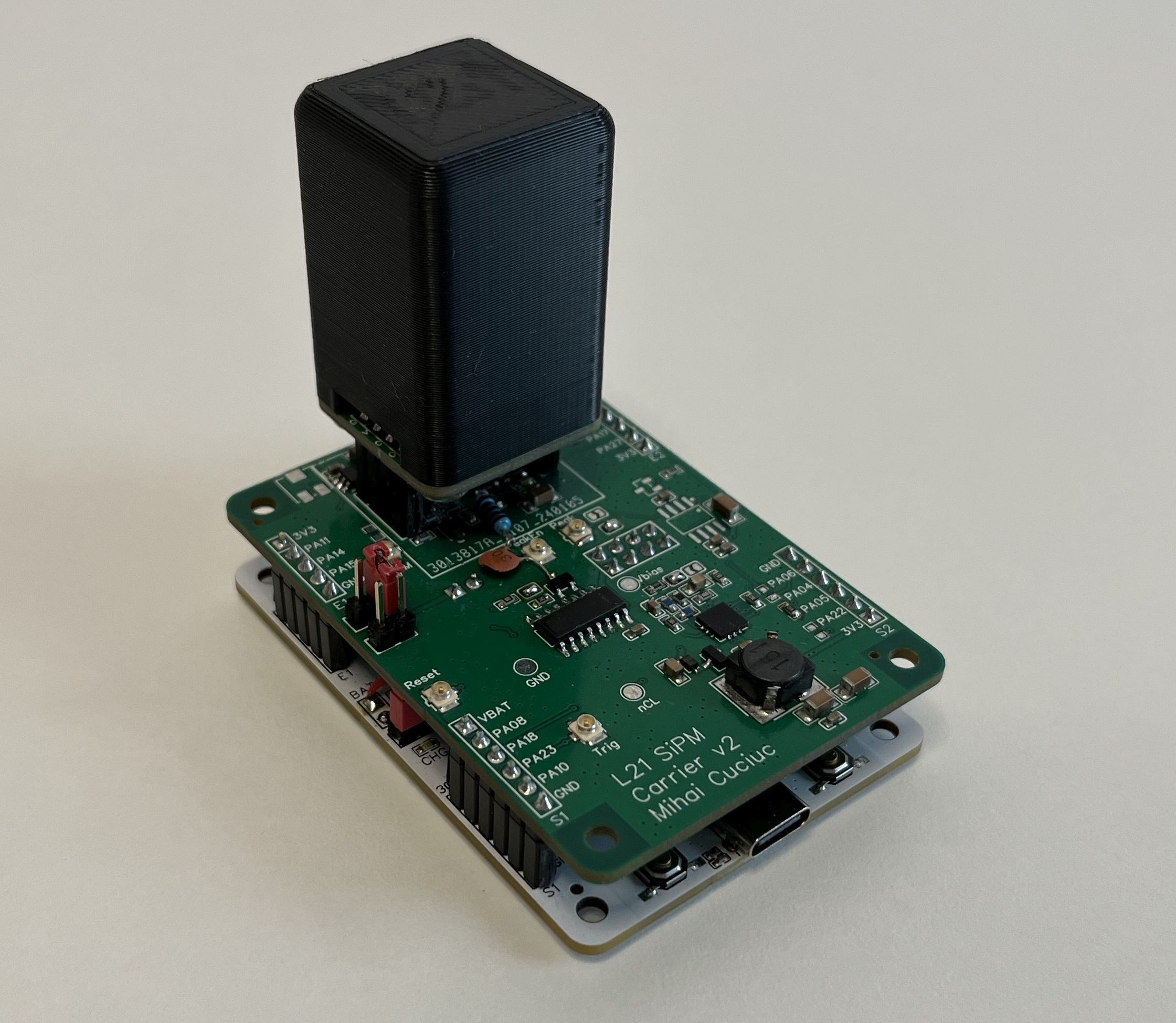
mihai.cuciuc
-
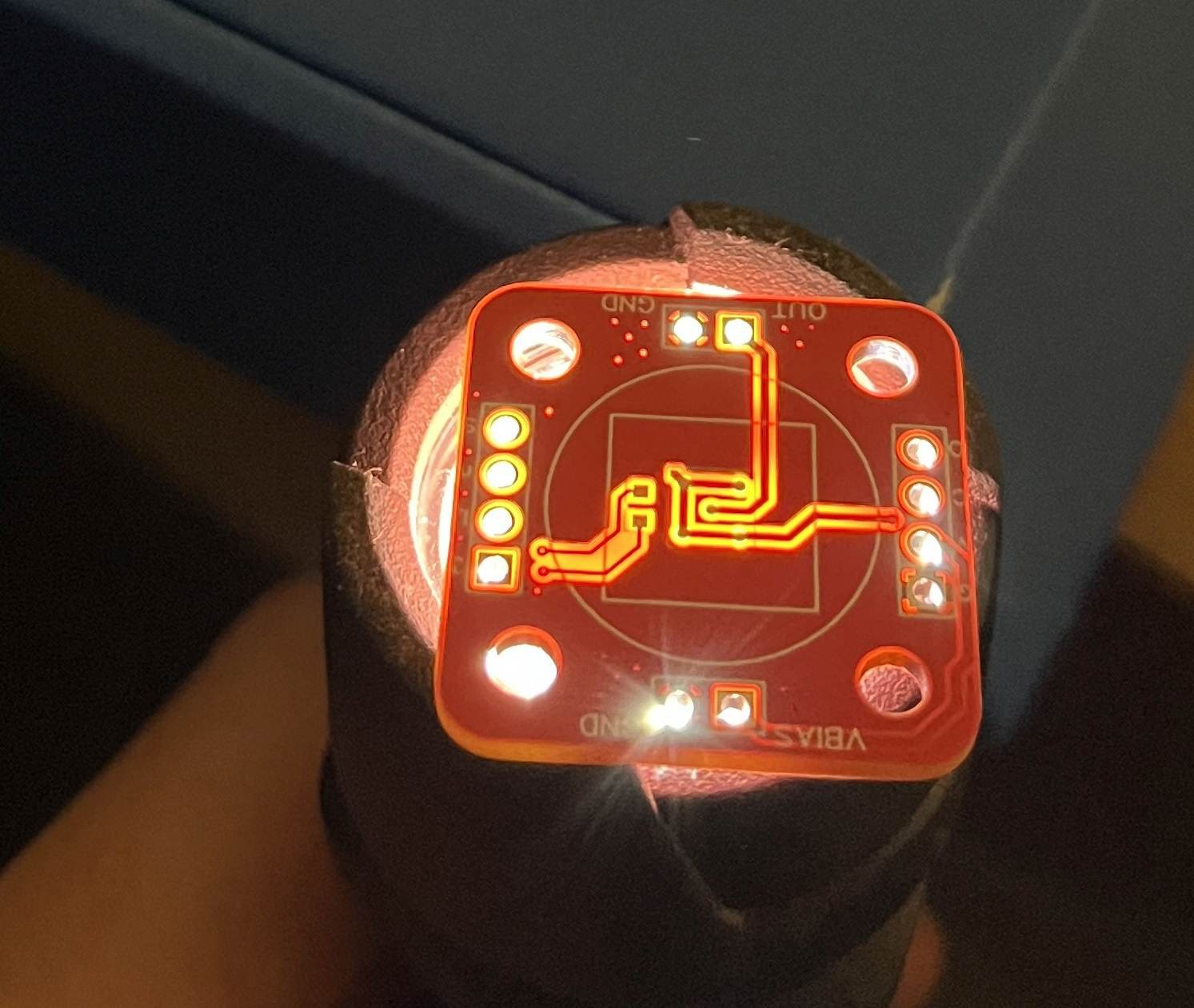
Analog PCB update with new bias supply
04/27/2024 at 08:13 • 0 comments![]()
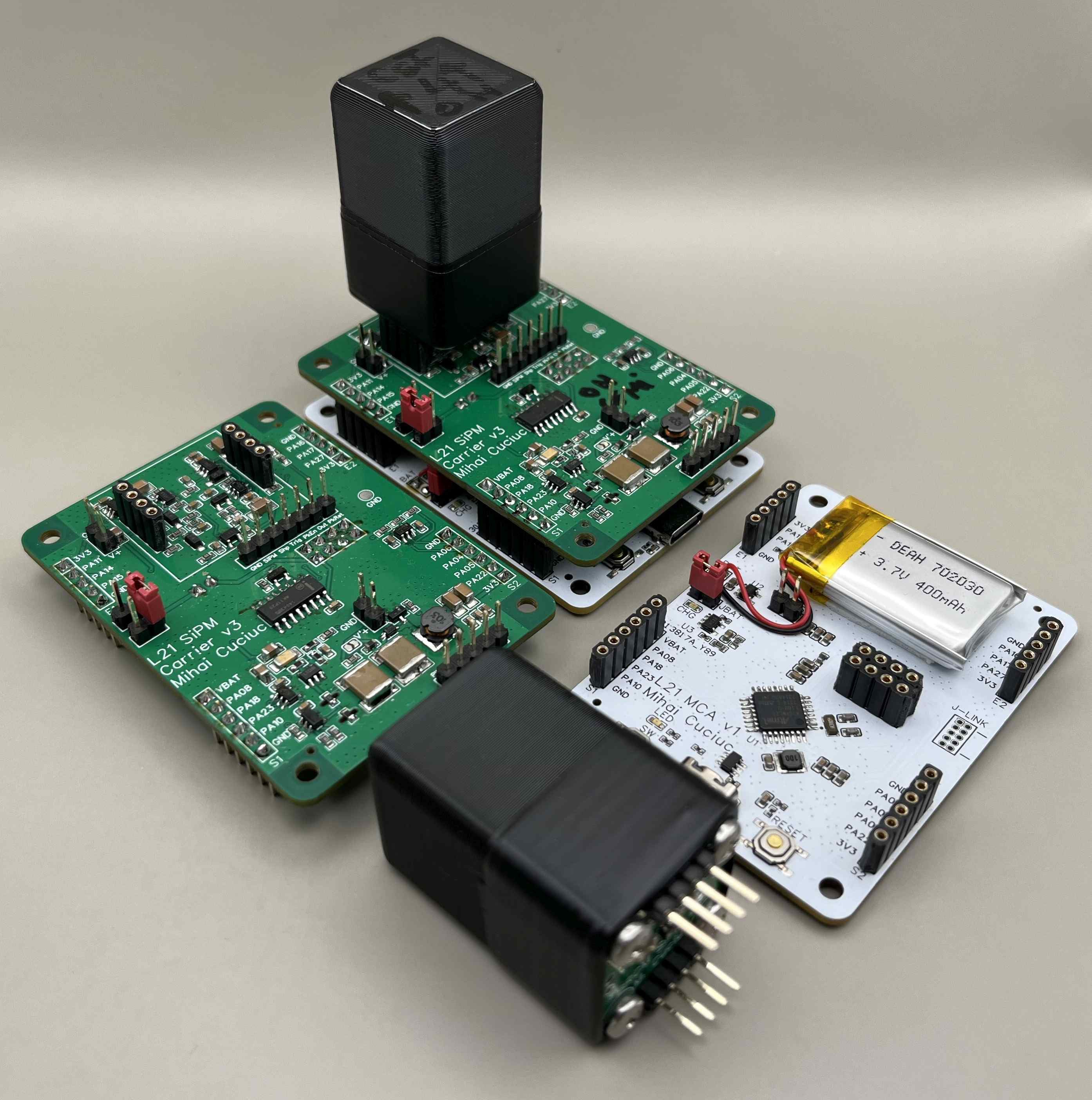
Assembled Pomelo (top), as well as its components: detector (bottom), analog board (left), and digital board (right)
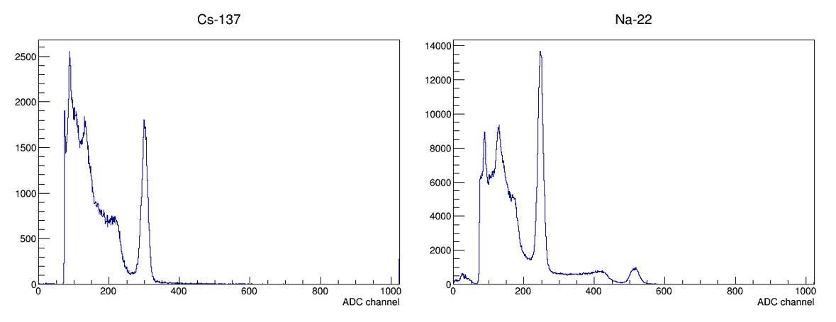
I integrated the new SiPM bias supply into the analog board. With this new version (v3) together with the 3cm^3 CsI(Tl) scintillator the results are pretty good:
- 2.6mA @ 3.3V in background conditions
- 4.3mA @ 3.3V with a 44 kBq Na-22 source on the detector
- <10% energy resolution @ 662 keV
The old version (v2) of the board with the same detector had the following:
- 6.3mA @ 3.3V in background conditions
- 7.6mA @ 3.3V with a 44 kBq Na-22 source on the detector
- <10% energy resolution @ 662 keV
![]()
Cs-137 and Na-22 spectra taken with the v3 board and 3cm^3 CsI(Tl) scintillator. Threshold was set very high, but it can be set below 60 keV
This updated PCB implements the new low power bias power supply and adds a ramp generator for calibrating the ADC. More details on ADC calibration in a following log.
-
Lower power SiPM bias supply
04/21/2024 at 09:59 • 0 comments![]()
Two PCBs to test different SiPM bias supplies. Left one is MAX1932 board, right one is a lower power version -- but it is a little worse and not as plug-and-play. This log entry describes its design and performances.
The MAX1932 is an excellent chip for biasing SiPMs, but I couldn’t get it to be low power enough for my application. It draws 4.35 mA from the 3.3V line while generating 41V for the SiPM. When switched off, it still draws 0.45 mA. As I’m targeting very low power consumption, I need better, even if I do end up paying with lower performance and increased circuit complexity. I designed a two-stage supply – a boost converter that generates some high voltage with very loose requirements on regulation, followed by a linear regulator that supplies the exact bias voltage needed by the SiPM.
Stage 1 – Boost converter
I was amazed by the performance of the Compact, low-power Geiger counter developed by BleakyTexwith an incredible attention to detail. He is using a custom boost converter to get to ~100V, and then a voltage multiplier to get to the ~400V that his Geiger tube uses. I decided to shamelessly steal his boost converter design, without the voltage multiplier. As I use a linear regulator afterwards, I don’t really care what the output voltage of the boost converter is. It's ok as long as it’s higher than the highest voltage I’ll need, and lower than what would fry the linear regulator. These loose requirements really help lowering the average power draw, as I can let the boost converter run to ~60V and switch it off until the input to the linear regulator drops below ~50V.
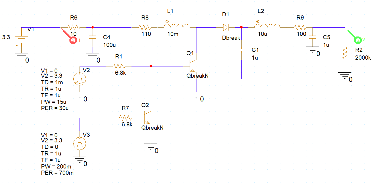
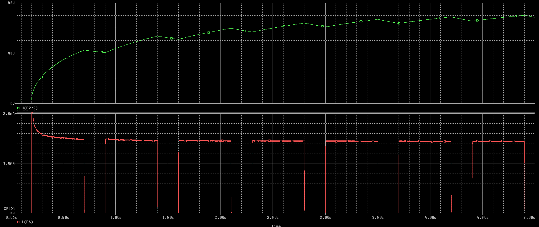
I don’t trust my math skills to do a similar analysis to the one BleakyTex did, but I did run a toy simulation in PSpice for TI.![]()
PSPpice for TI simulation schematic for the boost converter. Red probe measures input current, green probe measures the output voltage. R2 is a load to draw ~35 uA, to account for LDO, feedback networks, and SiPM.
In the simulation R6 and C4 form a filter such that I can measure the average current being drawn by the converter. Transistor Q1 does the switching at 33 kHz. To simulate what happens when the converter is running or stopped, Q2 sometimes pulls the base of Q1 to GND, thus stopping the converter.. This happens for 200 ms every 700 ms. L2, R9 and C5 smooth the output. The simulation results are in the following plot.
![]()
Top green plot is output voltage, steadily increasing over 5 seconds to ~70V. Bottom red plot is current drawn from the 3.3V supply, settling below 1.5 mA when the boost converter is running.
This voltage is fed to a linear regulator to supply the SiPM bias voltage.
Stage 2 – Linear regulator
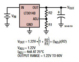
I chose the LT3014B LDO as it can take up to 80V on its input and draws less than 10 uA. Its output can go as high as 60V which is great because the Broadcom SiPMs I use need somewhere between 32V and 48V. The only problem is that I want to tune the bias voltage on the SiPM from software, and this LDO’s output is fixed by a resistive divider:
![]()
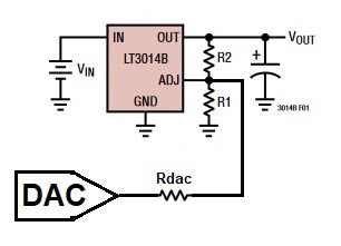
However, if I give the ADJ pin a little nudge with a DAC I can make the feedback loop settle at a different Vout:
![]()
This circuit has Vout = Iadj*R2 + 1.22V*R2/R1 – (Vdac -1.22V)*R2/Rdac. Choosing R1 = 180k, R2 = 5.6M, Rdac = 750k I get:
- Vout = 48V for Vdac = 0V
- Vout = 33.4V for Vdac = 2V
Putting it together
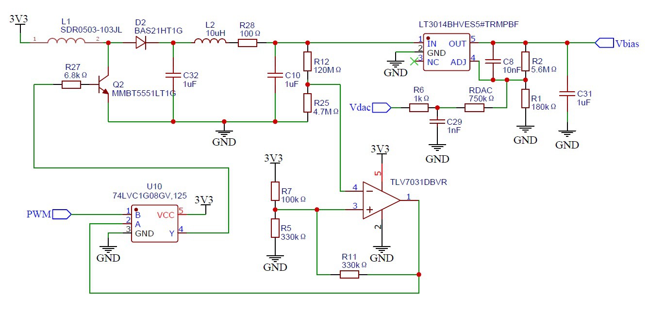
To make the boost converter run I use a 32 kHz output from the MCU, as it runs off an oscillator that has to run all the time anyway for timekeeping. This signal is gated by a comparator that keeps the output voltage within some reasonable limits. Using a single comparator with hysteresis keeps the part count as low as possible. The power supply design ends up looking like this:
![]()
Low power SiPM bias supply. The boost converter requires a 32 kHz square wave input and keeps its output swinging around 50 - 60V. The linear regulator's output voltage can be adjusted by a voltage input at the Vdac node.
The TLV7031 is a very low power comparator. Resistor R11 implements hysteresis to allow the input voltage to swing quite a lot before toggling the comparator output. The 74LVC1G08 is an AND gate that effectively enables or disables the switching regulator based on the voltage at the input of the LT3014B.
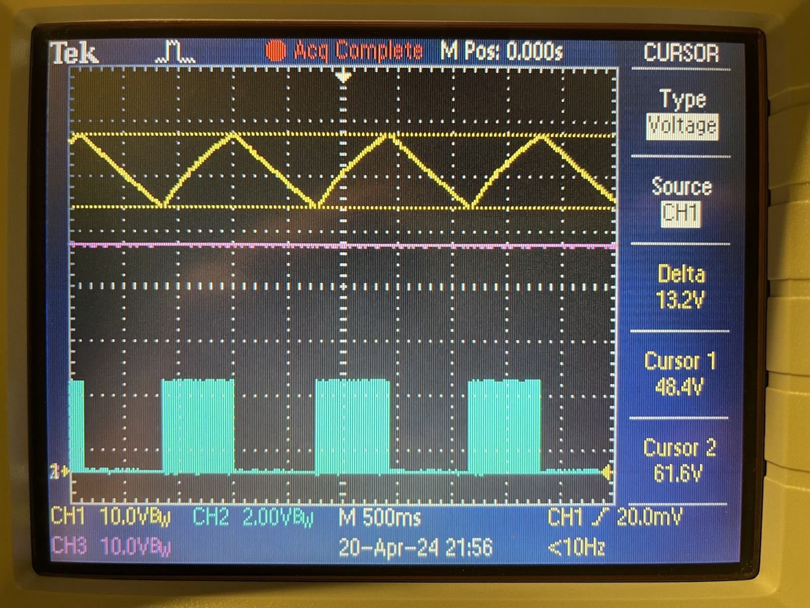
In this configuration the MCU retains full control of the bias supply without having to do any housekeeping once it's set up.A scope picture of the circuit in action shows the boost output, LDO output, and the PWM bursts that feed the switching transistor. The circuit struggles a bit harder than in the “Measurements” section below because of the two prodding 10 Meg scope probes.
![]()
Ch1: Boost regulator output, swinging from 48V to 61V
Ch2: PWM bursts, output of AND gate
Ch3: LDO output sitting at 41VMeasurements
The SiPM bias power supply draws an average of about 600 uA while generating 41V with no load. The average increases to 650 uA with a SiPM connected. This average is the result of the circuit drawing 2.1 mA for about 500 ms while the boost converter is running, and then ~20 uA while it's off. The ~20 uA result from the comparator, resistive divider R7/R5, and AND gate.
These numbers do not include the MCU internals that need to be kept enabled for the supply to run, i.e. 32 kHz square wave generation and DAC. The square wave should be very low power, but I measured two DAC channels drawing ~600 uA. I estimate less than 1.5 mA for the entire circuitry for generating the SiPM bias voltage – much less than the MAX1932. Where my solution does struggle however is with high count rates when the SiPM draws more current. I’ll need to adjust the PWM parameters to increase the current capabilities, but I should be able to do this on the fly, as needed.
-
Analog board
04/17/2024 at 05:23 • 0 comments![]()
I integrated the analog front-end and the MAX1932 power supply into one single plug-in analog board that the detector can then be plugged into. I used this together with the 10mm x 10mm x 30mm CsI(Tl) crystal to form a system with the following performances:
- Energy resolution @ 662 keV: less than 9.5%
- Current draw @ 12CPS: 6.5mA
- Current draw @ 2300CPS: 7.7mA
Analog front-end
This is the circuit simulated in the Analog Front End log entry. It has two RC stages, a fast decompensated op-amp with low current requirements, another RC stage, and then it goes to the peak detector. The first op-amp of the peak detector is an OPA357 that draws quite a lot of current. The second one, a voltage follower, is a low power part, as it can take all the time in the world until the ADC is ready to digitize the signal. To save power, the peak detector op-amps are only enabled when there’s a signal to be measured, thus saving a lot of power. The OPA357 needs to respond very quickly to an incoming enable signal, and the datasheet provides a turn-on time of 100ns. PSpice for TI simulations showed that there are several hundred ns available.
Trigger
The threshold for measurement is set by the MCU through its DAC, setting the minimum pulse amplitude to trigger a measurement. A fast, low-power comparator (TLV3201) supplies this trigger signal that gets sent to the peak detector op-amps enable pins to switch them on, and also to the MCU to wake it up and start a measurement. To keep the peak detector active for as long as needed by the MCU, the trigger signal goes through an S/R latch that is only reset by software. As the low-power S/R latch used (MC14043) quotes propagation delays as long as 350ns at 5V, there is a fast bypass for this signal with a diode-OR between the latch output and the incoming trigger signal.
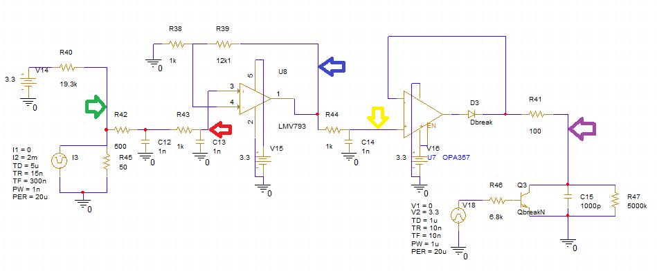
Validating the simulations
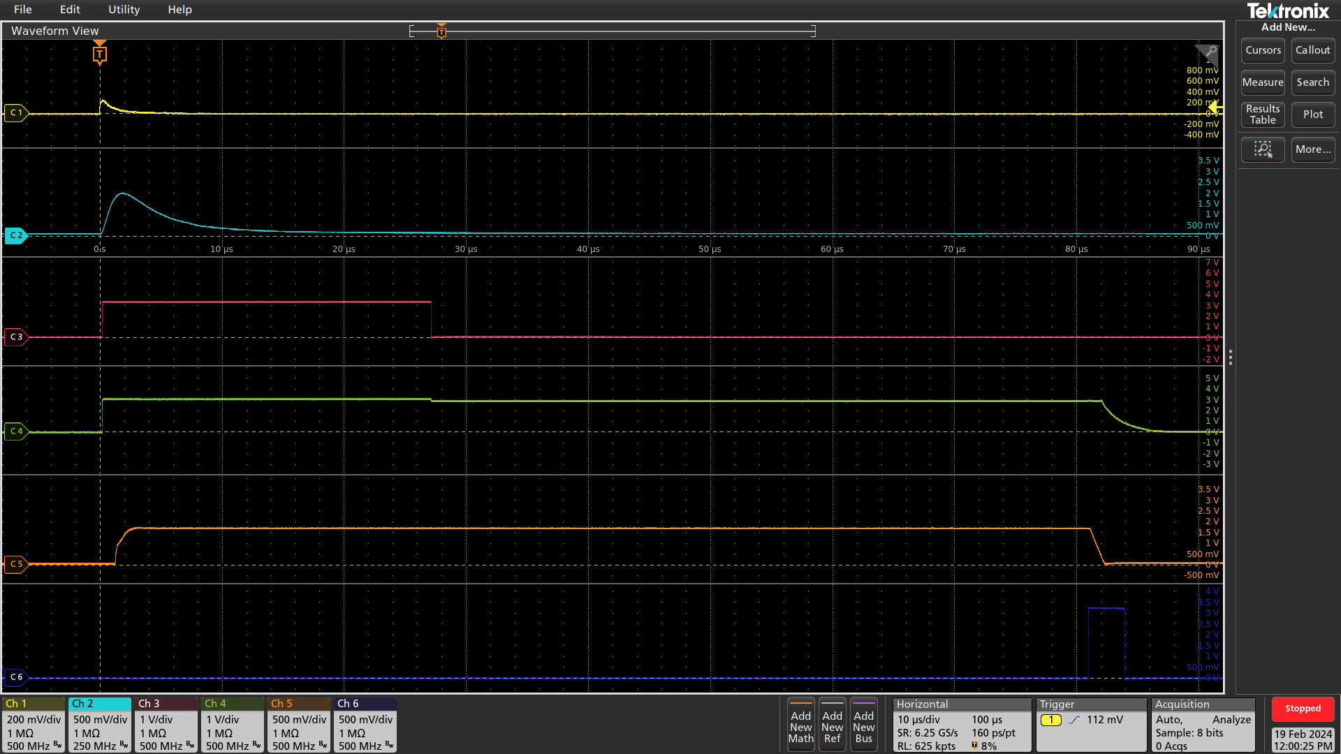
The board has multiple analog test points that make it easy to trace the functionality of the device and check against PSpice for TI simulations, with an example in the figure below.
![]()
Ch1: SiPM output
Ch2: Shaper output. It is sent directly to trigger comparator. It goes through another RC filter before being sent to the peak detector
Ch3: Trigger comparator output
Ch4: Peak detector enable. This is diode-ORed between trigger comparator output and the output of an S/R latch that is set by the trigger comparator. This ensures fast propagation of the signal to enable the peak detector (S/R latch propagation delay is several hundred ns) and also that the peak detector won’t switch off unless told so by software
Ch5: Peak detector output. This signal goes to ADC
Ch6: Peak detector reset. This signal clears the peak detector capacitor. While it’s set the peak detector is also disabled through the S/R latch.The entire measurement takes ~85us, but I tracked some of the time spent in the interrupt handler mechanism which has to check every external interrupt line. I could hack a way around this to bring the measurement to ~45us.
-
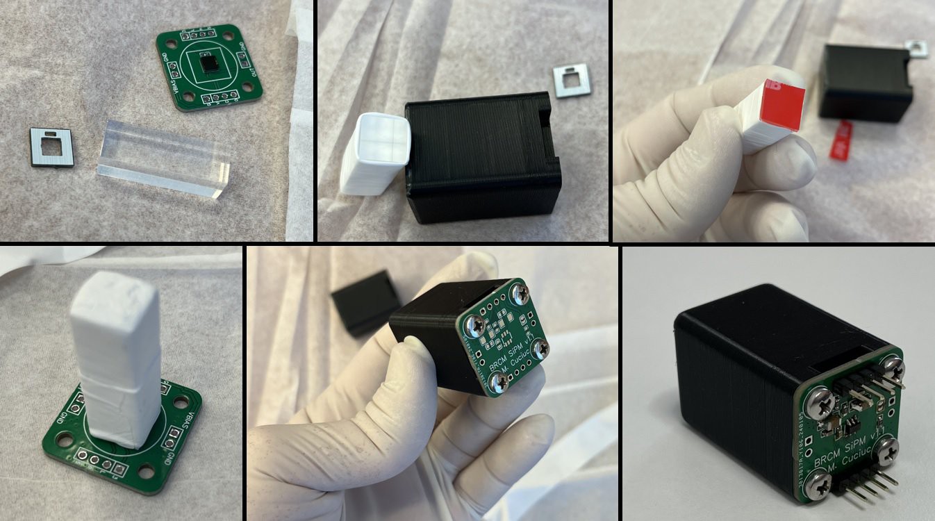
CsI(Tl) scintillator, 3cm^3
04/16/2024 at 04:34 • 0 commentsCsI(Tl) is a commonly used scintillator with good energy resolution because it has a very large light yield, around 54 photons per keV. It is slightly hygroscopic but not enough to cause serious concern for testing. I have 10mm x 10mm x 30mm CsI(Tl) crystals that I wrapped in Teflon and used clear 3M VHB tape for coupling them to the SiPMs. A black 3D printed housing for the crystal acts both as mechanical protection but also as a light shield.
![]()
Directly underneath the SiPM on the PCB there is a high accuracy SPI temperature sensor (TMP126). The SiPM gain depends on temperature and can be compensated for by adjusting the bias voltage. However, this functionality is not implemented in firmware yet.
-
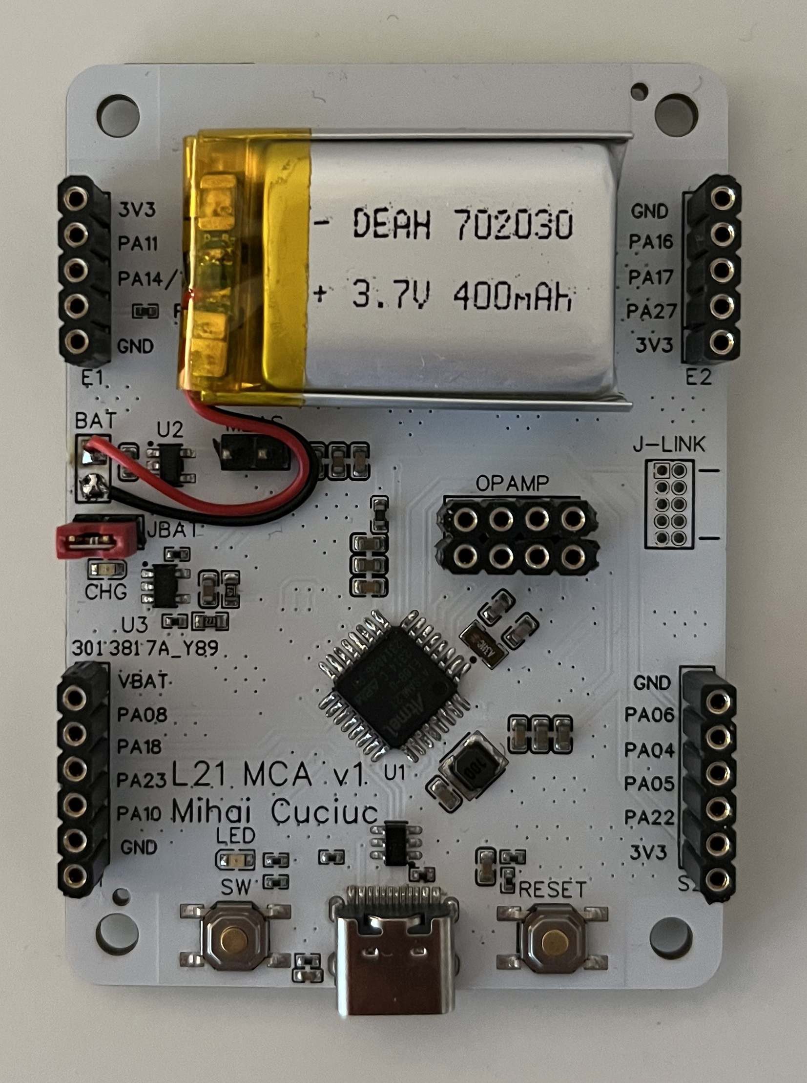
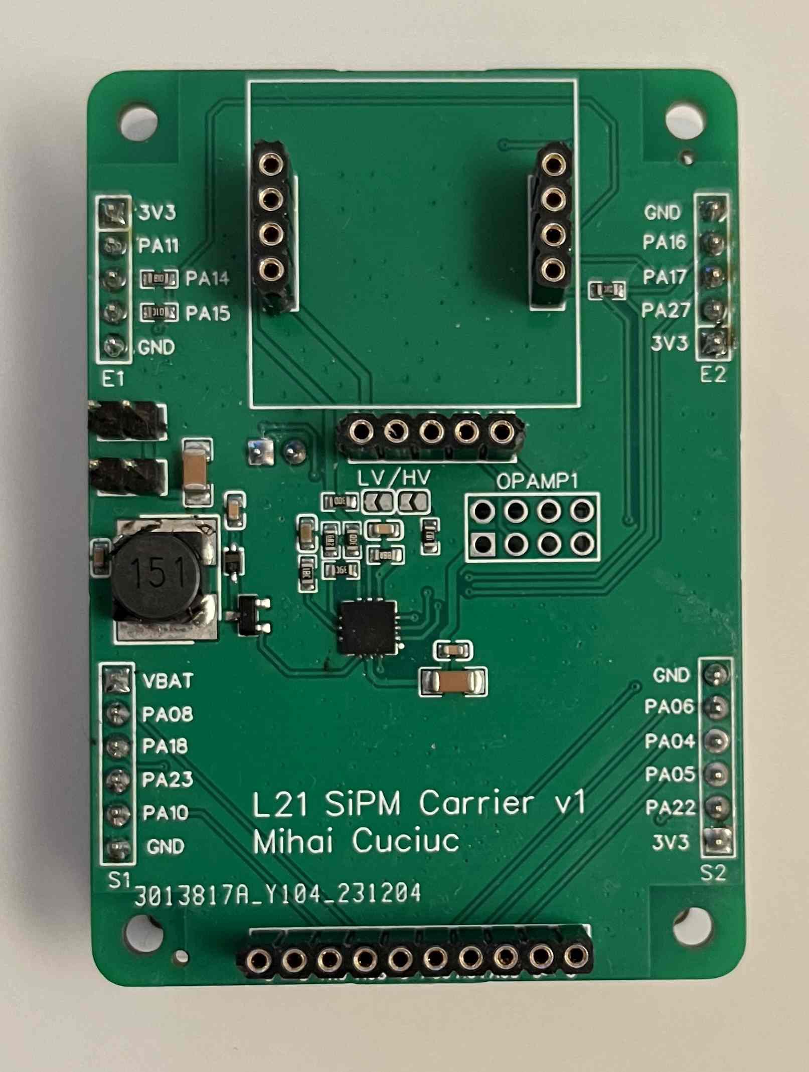
Digital board
02/20/2024 at 05:58 • 0 commentsFor the digital section I went with the Atm… erm, Microchip ATSAML21E18B as I already had a previous project centered around it. It’s capable of low power operation and is packed with both analog and digital peripherals that make it quite versatile. It’s got USB and I adapted this UF2 bootloader to run on my board which makes development a lot easier.
![]()
Features
- Most of the pins broken out to headers
- On-board Li-Ion battery charger - Microchip MCP73832. It can be disabled for use with non-rechargeable batteries
- Power jumper. Can be used to measure current on the 3V3 line
- Type-C port with TVS diode protection
- User LED and button
- Reset button & circuitry
- Header close to MCU for pins connected to the internal opamps
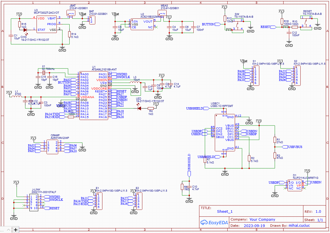
Schematic
![]()
-
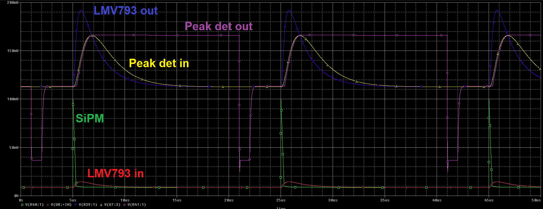
Analog Front End
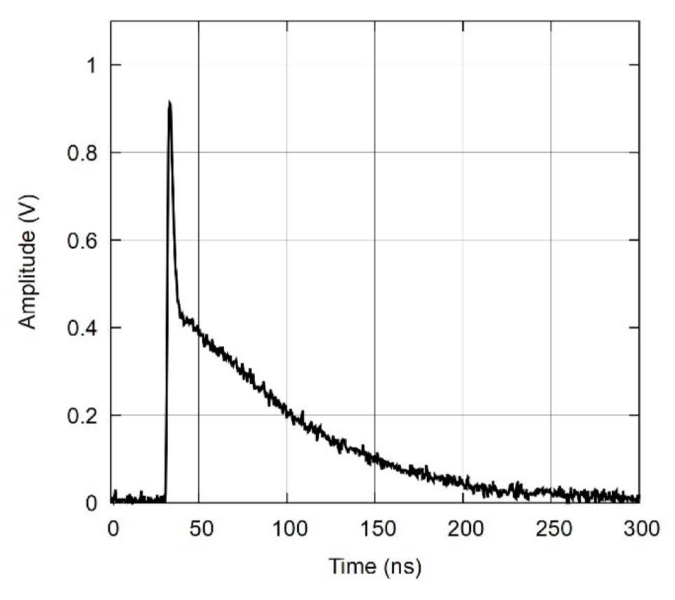
02/07/2024 at 06:04 • 0 commentsSiPM pulses have fairly large amplitudes so don’t need a lot of amplification, but they have fast rise-times below a few ns and decay times in the range of hundreds of ns. The figure below is an example pulse provided in the Broadcom AFBR-S4N44P014M datasheet.
![]()
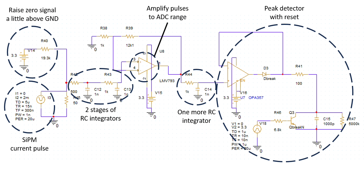
The easiest way to digitize its amplitude with a slow ADC would be using a very fast peak detector that can handle the high frequency content of the rising edge. But this wouldn’t be very low power as the peak detector has to be constantly enabled to catch pulses, and fast op-amps draw high current. My approach is to “round off” the pulses using RC integrators to slow them down, and then triggering on this slow version of the pulse to enable a peak detector before this pulse reaches its maximum. While this sounds easy, it was my first attempt at some analog design so I ended up spending a few days simulating it in PSpice for TI. This is the schematic I ended up with in the simulation, with components grouped into functional blocks that are described below.
![]()
SiPM
I simulate the SiPM as a current source that produces a pulse with a shape that approximates what I measured on the oscilloscope. The limited bandwidth of my measurement setup made the rising edge less steep so I generate a pulse with a 15ns rise time and 300ns fall time. The current amplitude is chosen to provide some hundreds of millivolts on a 50 Ohm resistor.
Raise zero signal a little above GND
This is just a resistor from 3.3V to inject a small DC offset into the measurement. The op-amp outputs in the system don’t go down to 0V, but have a minimum output voltage of 100mV or so. So this is a very simple solution to cope with that. It does cost a little though – the ADC input DOES go to 0V, so I lose a little bit of ADC range.
2 stages of RC integrators and another stage after the first op-amp
These round off the sharp input pulse to much slower pulses. There are two tradeoffs though. One is that you lose amplitude, but you can easily recover that using subsequent amplification stages. The second tradeoff is that in high count-rate applications you can get pulse pile-up, where the detector provides another short current pulse before the integrator output reached down to zero -- and that makes your measurement wrong. Serious analog processing uses a series of CR differentiators and RC integrators together with pole-zero compensation networks to create nearly gaussian pulses.
Amplify pulses to ADC range
The LMV793 is a decompensated op-amp. This means it’s much faster than op-amps with similar power requirements, but it’s not unity-gain stable. It only works at high amplification, in the LMV793’s case more than 10x. This is the only place in the circuit that allows for some flexibility in setting the gain, apart from the bias voltage on the SiPM. Thus this gain is set to match the gamma spectrum range to the ADC range. As this op-amp needs to be constantly powered it will significantly contribute to the total system power draw -- the LMV793 is spec'd to draw at most 1.65mA so it should fit in my power budget.
Peak detector with reset
This is just half of the peak detector circuit. Another unity gain buffer follows, but for this simulation it’s unnecessary. The 100 Ohm series resistor is there to make the op-amp happy driving a capacitive load. The OPA357 has an enable input (not used in this schematic) that can turn the op-amp on in 100ns. So as long as the trigger pulse is generated well in advance the peak detector should consume no power until it’s actually needed. And then after reading the stored value it can be shut down until the next pulse. This section of the simulation also contains a pulsed source that periodically resets the peak detector such that I can simulate several pulses.
Most peak detector designs use identical op-amps for both the ideal diode as well as the unity gain buffer (that is not included in this schematic). This allows those designs to use fancier feedback loops that minimize capacitor discharge or improve response to short peaks. However I decided to keep the loop simple because I was afraid of circuit behaviour when enabling both op-amps and then expecting a valid result in a few hundred ns. Keeping separate feedback loops for the ideal diode and the voltage follower allows one to treat them independently. Additionally the voltage follower can now be a much slower op-amp that even when active will draw very little power contributing a little to making a low power design. I decided for a TLR341G for this.
I used two great resources for understanding what I'm doing while designing this section:
EEVblog's video on peak detector circuits
Section 4.5.1 from The Art of Electronics, 3rd Edition
PSpice for TI simulation
To validate all of this I ran some simulations with different pulse amplitudes to confirm the system behaves linearly. Below is the schematic with the color-coded probe points, as well as the simulation results.
![]()
![]()
Conclusions
Not included in this simulation is the trigger section. A comparator triggers on the LMV793 output and enables the peak detector. Simulations shows that there are several hundred ns between the LMV793 output rising above a set threshold and the peak detector input reaching its maximum, thanks to the additional RC integrator in between the two. So this whole thing should work.
These integrators do pose a limit on how closely spaced pulses can be. One can see the peak detector input returns to baseline in ~15us so this will not properly handle very high count rates. I expect ~20 kCPS (to account for statistical fluctuations) should be doable without messing up the energy resolution.
-
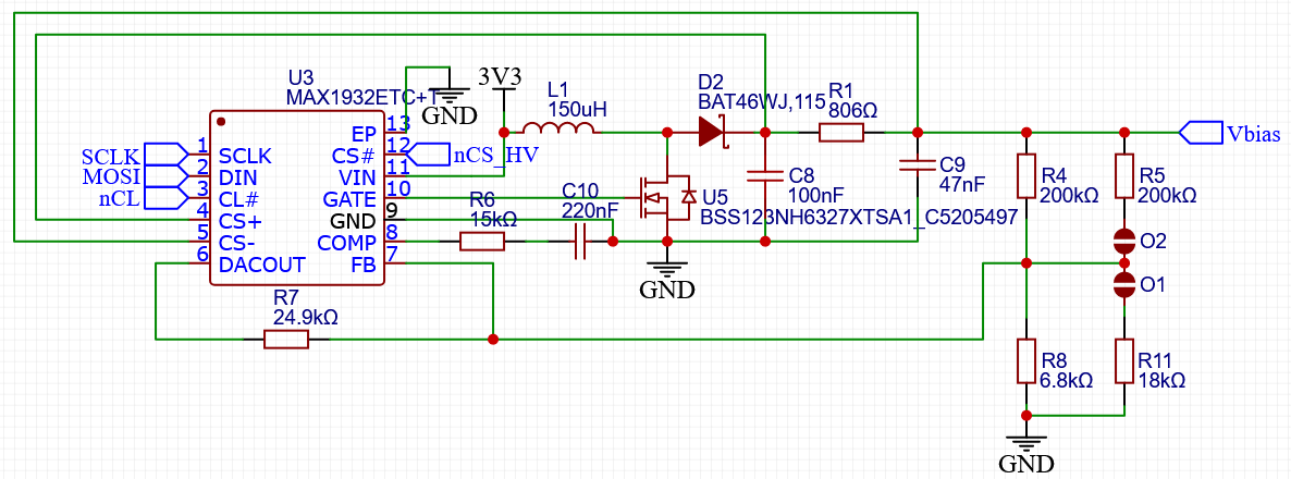
SiPM bias power supply
01/25/2024 at 05:28 • 0 commentsThe CosmicPi project uses a very nice chip for biasing SiPMs, the MAX1932. It can be configured to output as much as 90V for powering SiPMs, and you can set the voltage within a programmable range using SPI. It’s not cheap, but it’s very cool.
![]()
The jumpers (O1 and O2) allow two output ranges: 25.5V..30.5V for Onsemi SiPMs, or 36.5V..48.5V for Broadcom ones.
![]()
The board works great for powering the SiPMs, but draws a bit more current than I'd be happy with, at ~9mA while supplying 31V. I certainly did not help with the feedback resistors that can draw up to 150uA @ 31V. Adding reverse current through diode, switching efficiency (0.5 hinted in the datasheet), and the 1mA operating supply current I'd expect about 4mA. Interestingly even with the chip in shutdown (DAC = 0x00) I'm seeing ~3mA being drawn.
But it's definitely good enough to allow me to develop the analog front-end for the SiPM which plugs into the horizontal headers on the PCB.
-
Silicon photomultiplier
01/21/2024 at 08:50 • 0 commentsPhysics overview
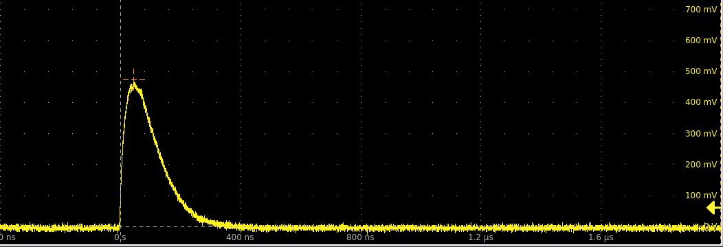
To convert the small number of optical photons into an electric signal a photodiode is not ideal. Short of using a photomultiplier tube (PMT) the best option is a silicon photomultiplier (SiPM). These are arrays of thousands of cells, with each cell being sensitive to a single photon. When a photon is absorbed by a cell it supplies a small pulse of current. If more photons hit the same cell at the same time, you won’t see any difference – the cell either fired or it didn’t. But since scintillators produce such a small number of photons it’s very likely that each one will strike a different cell. All these small pulses of current are added up and you get a signal that is proportional to the number of cells that fired.
![]()
Oscilloscope trace of SiPM signal from scintillation event Each cell is a small photodiode that is built to be operated above its breakdown voltage. That makes them super unstable, and once a photon is absorbed, the diode breaks down generating that pulse of current. The cell has a series quenching resistor that causes the voltage across the cell to drop during breakdown ending the pulse and effectively resetting the cell.
Since cells are so unstable, they also fire randomly, due to thermally-generated carriers. This leads to a “dark count rate” of the order of millions of counts per second but as these pulses don’t overlap you only see them as an increased noise floor.
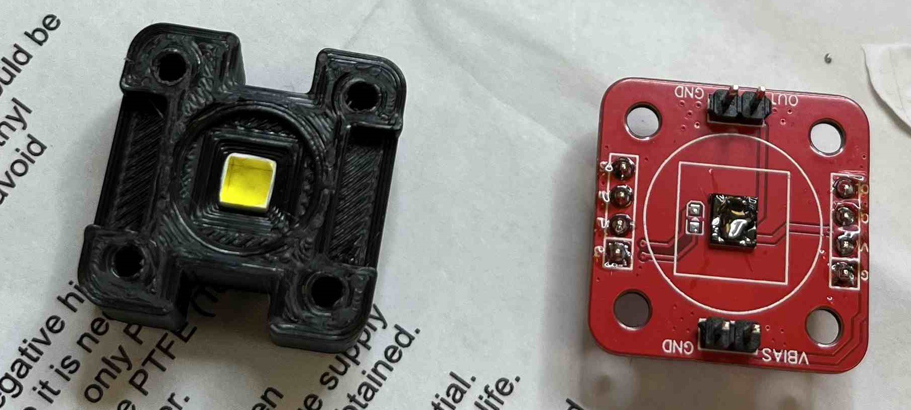
Detector assembly
![]()
To make the most out of the small number of scintillation photons the optical coupling between scintillator and SiPM has to be as good as possible. Changes in the index of refraction, as can be generated by small pockets of air at the interface between the two, can cause photons to be reflected away from the detector. This is only made worse if the optical contact is uneven across the detector surface. A common solution to this problem is optical grease, having a known index of refraction, that can be applied similarly to how thermal paste is used on CPUs to improve thermal conductivity.
Because of light leakage through the PCB I had to wrap the assembled detector in black electrical tape.
Pomelo
I used the Broadcom AFBR-S4N44P014M 4mm x 4mm (ish) SiPM since it’s fairly low-cost and comes in a reasonable package for soldering with a heat gun. It needs to be operated between 38V and 48V.
Testing the fully assembled detector (wrapped scintillator, case, SiPM, power supply) with a digitizer at work I could get a feel for the expected performance before I started agonizing over my own readout electronics.
![]()
-
Scintillator
01/18/2024 at 05:30 • 0 comments
Two GAGG(Ce) and three LYSO scintillator crystals next to a TO-92 transistor for size comparison Physics overview
When a high energy photon (a gamma ray) is absorbed by a scintillator some visible photons are emitted. These visible photons have a fairly fixed wavelength, but the number of photons is proportional to the energy of the gamma ray. This number is in the range of tens of photons per keV, so for a 662 keV gamma ray coming from Cs137 hitting a CsI(Tl) scintillator you get ~36000 optical photons. For a 59 keV gamma ray from Am241 you only get about 3000. This is a statistical process so the numbers vary, giving rise to limited detector resolution – the full energy peak of a monoenergetic gamma ray will appear as a broad distribution in the detector. The optical photons are emitted in all directions from the point of interaction in the crystal, and there may be multiple such points (e.g. if the gamma ray suffers Compton scattering within the scintillator and the resulting lower energy gamma ray is also absorbed).
Important properties of scintillators are light yield (optical photons per keV), density, and atomic composition. High density materials containing elements with a high atomic number are preferred as they have a higher probability that the gamma ray will interact with the scintillator and not let any of the deposited energy escape the scintillator.
Detector assembly
Since the scintillator emits a pretty small number of photons and they can originate anywhere in its volume, it is important to try to reflect as many of these as possible towards the detector. This can be done either with specular (mirror-like) as well as diffuse (matte) reflection. It’s very common to wrap the scintillator in plumber’s tape (Teflon).
Also because of the small number of optical photons you’ll want to keep any stray light from entering the detector as this will completely overwhelm the scintillation photons. You’ll sometimes see people in labs placing several layers of dark heavy clothes over detectors when these are not light-tight by design.
Pomelo
![]()
Scintillator wrapped in Teflon and placed in light-tight enclosure before being assembled on SiPM PCB ![]()
I used a 4mm x 4mm x 10mm GAGG(Ce) crystal wrapped in Teflon tape and placed in a black 3D printed holder. I was hoping the PCB would provide enough light-tightness on the bottom but some light ended up coming through the PCB material around traces that did not have copper pour behind them. The picture on the right shows an extreme case with a flashlight shining through the PCB. Enough photons to disturb the measurement came through even in ambient lighting conditions.
Pomelo: Gamma Spectroscopy Module
A complete low-power gamma ray spectrometer that can be used by itself or integrated into other projects