sky-guided
-
#11: Design deficiencies, and what you can improve
08/28/2024 at 00:49 • 2 commentsI'm considering this project Completed, at least for the time being. I'm incredibly proud of what I've created -- every design goal was achieved, and it looks even better than I'd dared to hope.
However, this is far, far from perfect. If I were to continue this project, I have a real hit-list of what could be improved.Overall System
The biggest issue is that controlling drive intensity by adjusting mosfet feedback bias voltage is janky and unstable. A proper system would leave a bias voltage set with a trimmer, and use high-side limiting on the primary input current for primary drive control. I realized this kinda late in the design process, and wanted to reach "done" rather than do another round of prototyping.
Also, having a breakout board for the USB-PD trigger module is pretty inelegant. Having a trigger module on-board would be better, but when I started this project I was having trouble finding a suitable IC with decent availability in the US. Several folks have since suggested good candidate ICs.MOSFET and driving
A straightforward error is that the gate-drive resistors have been undersized. The design shown in the video uses two 10-ohm 1206-size resistors in parallel (per mosfet), and they get incineratingly hot if there's no ionization/plasma to load the circuit. For the published release version, I increased those to a pair of 1-watt 2010-size resistors which should hopefully fare a bit better.
I probably ought to be using an asymmetric resistor / diode pair on the gate pins. Almost wish I'd investigated that sooner since the footprints are already there, but, hey, like I said I'm declaring this project Done.More generally: I'm convinced my mosfets are running hotter than they really ought to be.
I still don't feel like I have a sufficiently deep understanding of mosfet switching behavior, especially when driven from a sine-wave rather than a proper square wave. Using two parallel mosfets for the final version was a callous attempt at reducing heating. In prototypes, heat was observed as being heavily dependent on how much current I was drawing and that made me hope that parallel would help, but I also should have known that I was looking at switching losses rather than anything Rds(ON) related. I did some quick math before going parallel which made it seem promising, but like I said there's aspects of mosfet switching that I'm still learning.
The most-correct version of this circuit would probably use an actual mosfet driver IC, with something like a PLL as part of a feedback loop. Would be lovely to have both a nice square-wave drive and finely adjustable phase offset.
Using something like a GaN mosfet might also perform a lot better!Arc Start
For the first start when the glass vessel is room-temperature cold, button-press arc-start reliability isn't as good as I'd like -- sometimes it does take several tries to get the toroid running.
This particular arc start method is too expensive. If I were designing for even small-run production, it'd get a major overhaul.
Both arc-start transformers and the GDT are all what I'd call "kinda-specialty components" which isn't ideal even if their BoM cost is modest. More seriously though, the flyback controller chip LT3420 is both expensive ($6.75/ea at qnty 10) and has limited availability. The good news is that the fancy chip is probably completely unnecessary. I initially thought I might be using the advanced functionality like keep-charged and the "done" signal, but the system I ended up with would probably be just fine with a fixed-duty-cycle flyback charger.
There's a lot of different ways of getting pushbutton arc start though. I know one person who reports success using a cheap aliexpress "arc ignitor" module with one leg of the output tied to ground and the other pressed up against the globe. Another promising idea which was suggested to me would be to have an entire autotransformer-style secondary winding driven by the primary inductor, which would offer the benefit of automatic start!
I'll continue to edit this post as I think of more improvements, and as improvements are suggested :)EDIT 2024-09-19
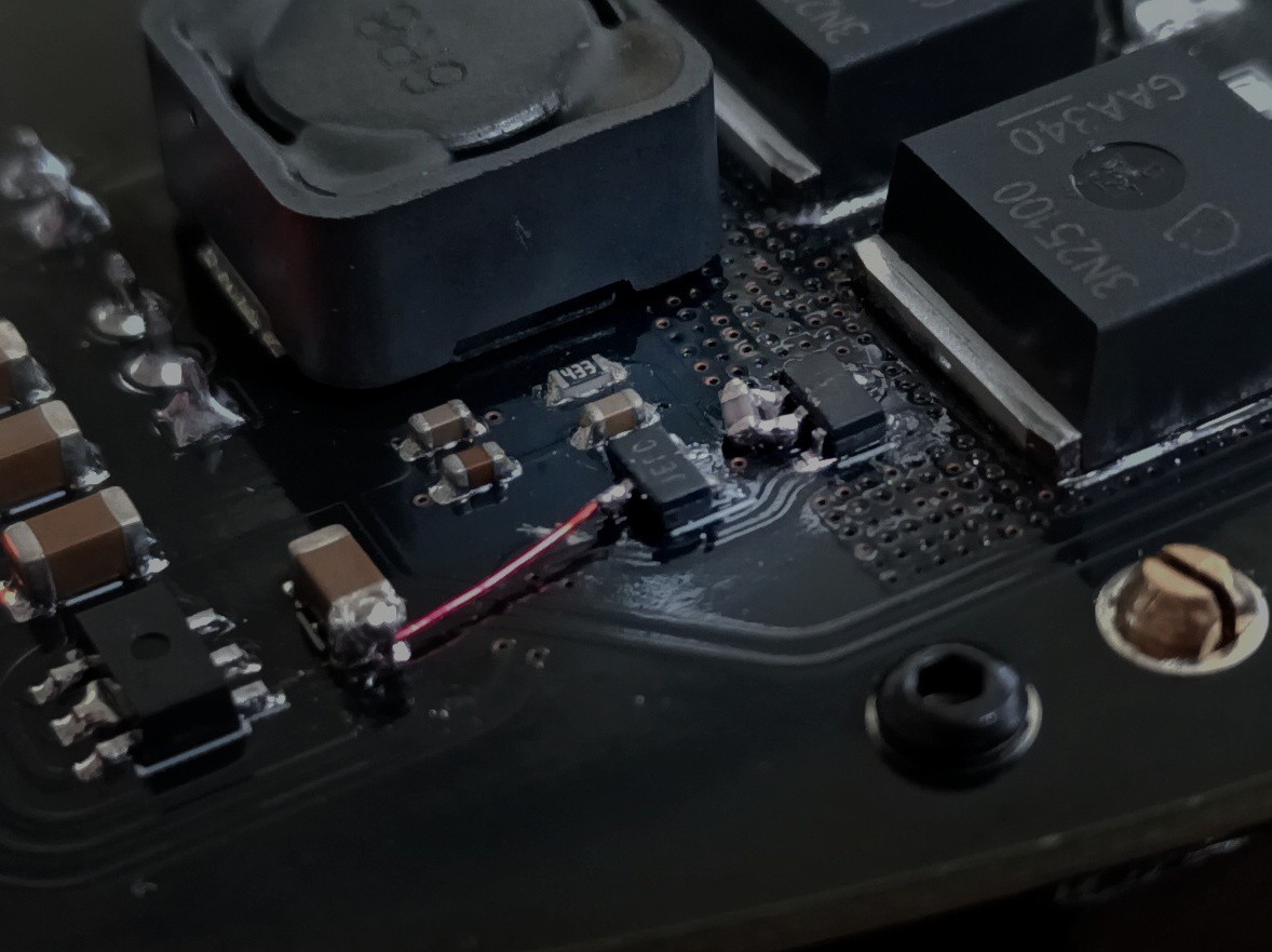
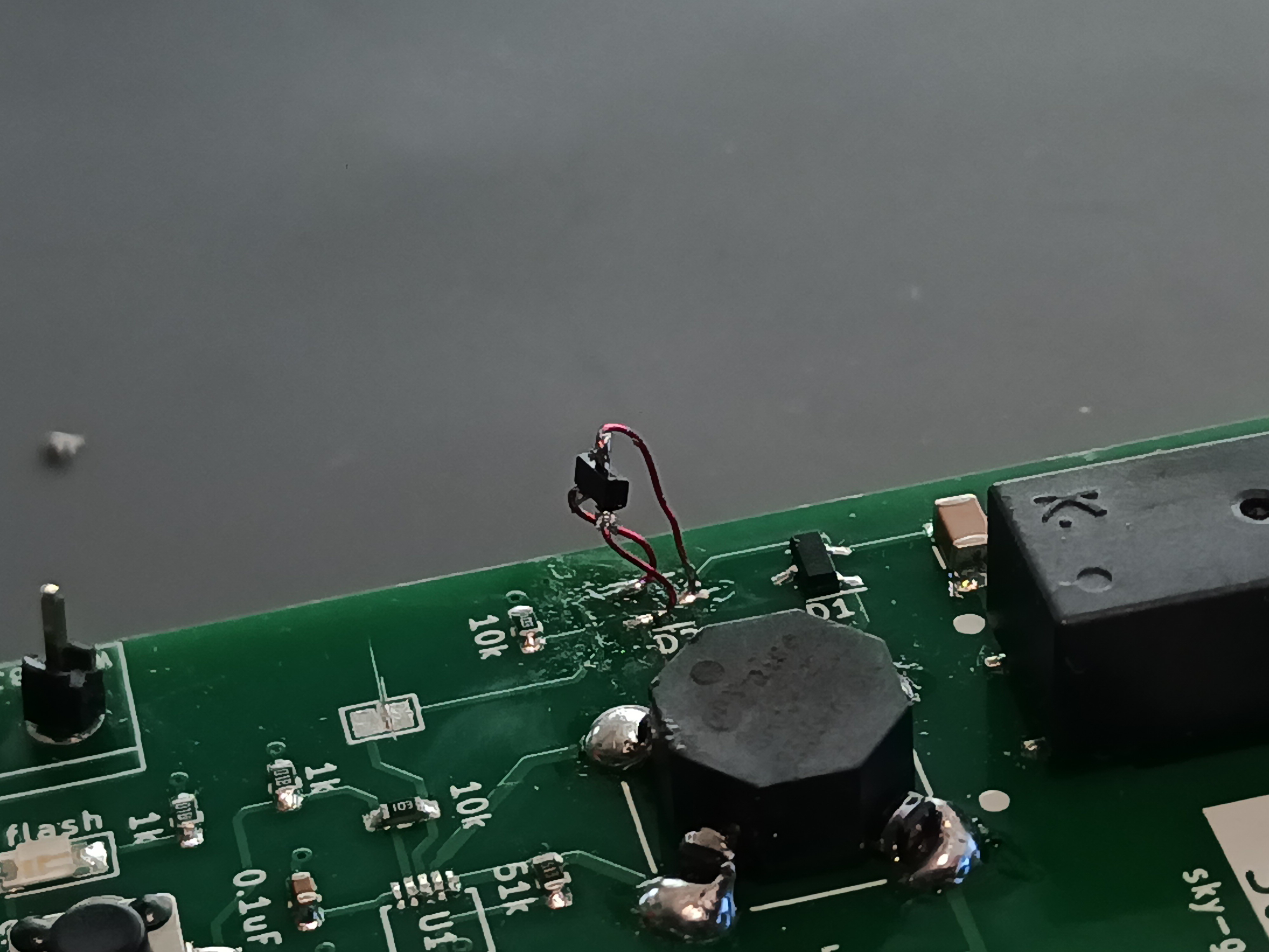
Matthew Sylvester assembled this project from the PCB, and let me know that they experienced arcing underneath the xenon flash trigger transformer. I've increased the clearances, and released the changes as v1.03
Double-checking against IPC 2221, the clearances still aren't "enough" but it's the best I could do without a redesign of the entire arc start section. -
#10: AND IT IS DONE
08/25/2024 at 22:31 • 0 commentsThanks for following along :)
-
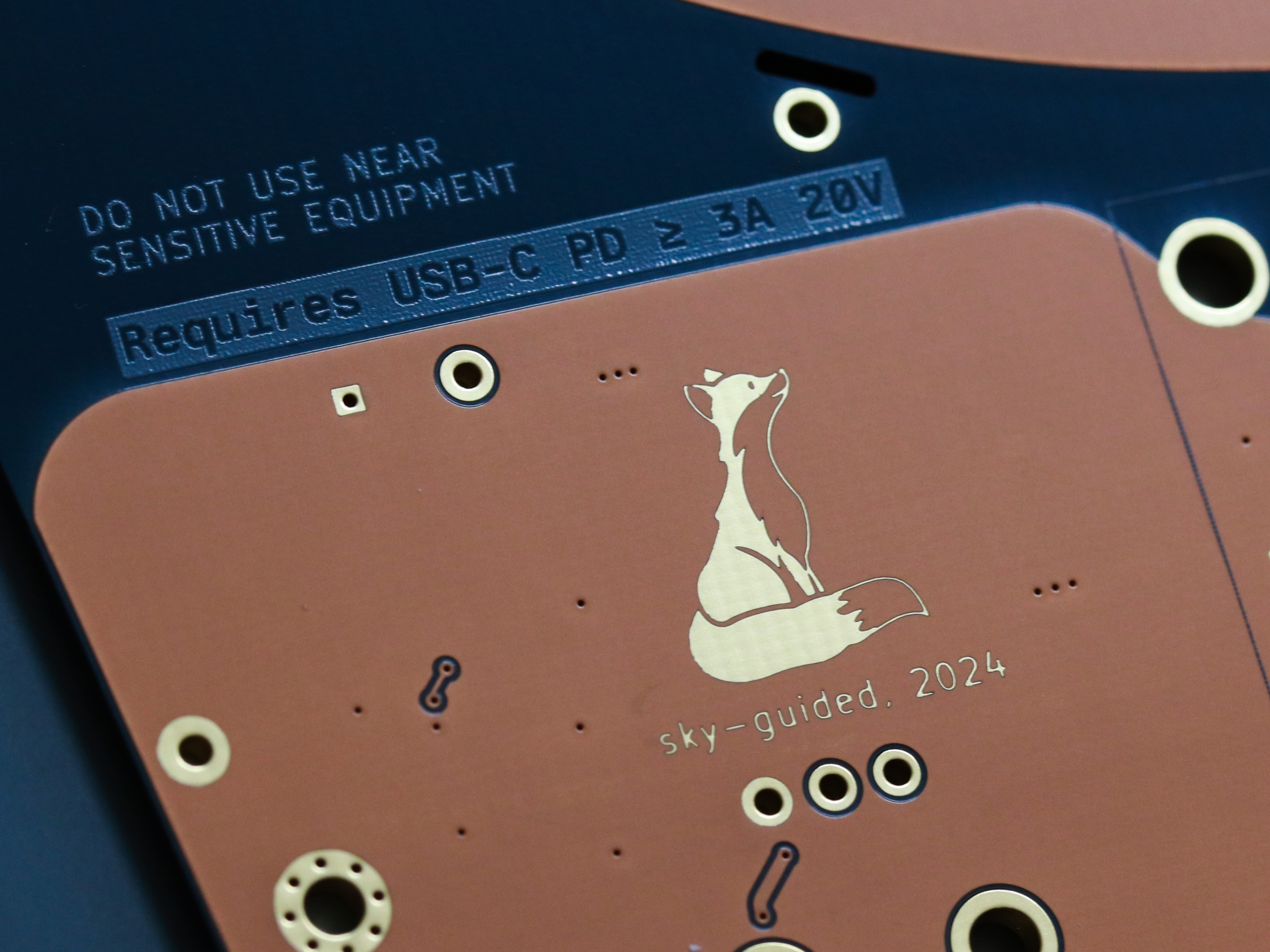
#9: Black FR-4 and transparent soldermask, by PCBWay
06/01/2024 at 21:33 • 1 commentFor the final build of this project, I wanted something special.
![]()
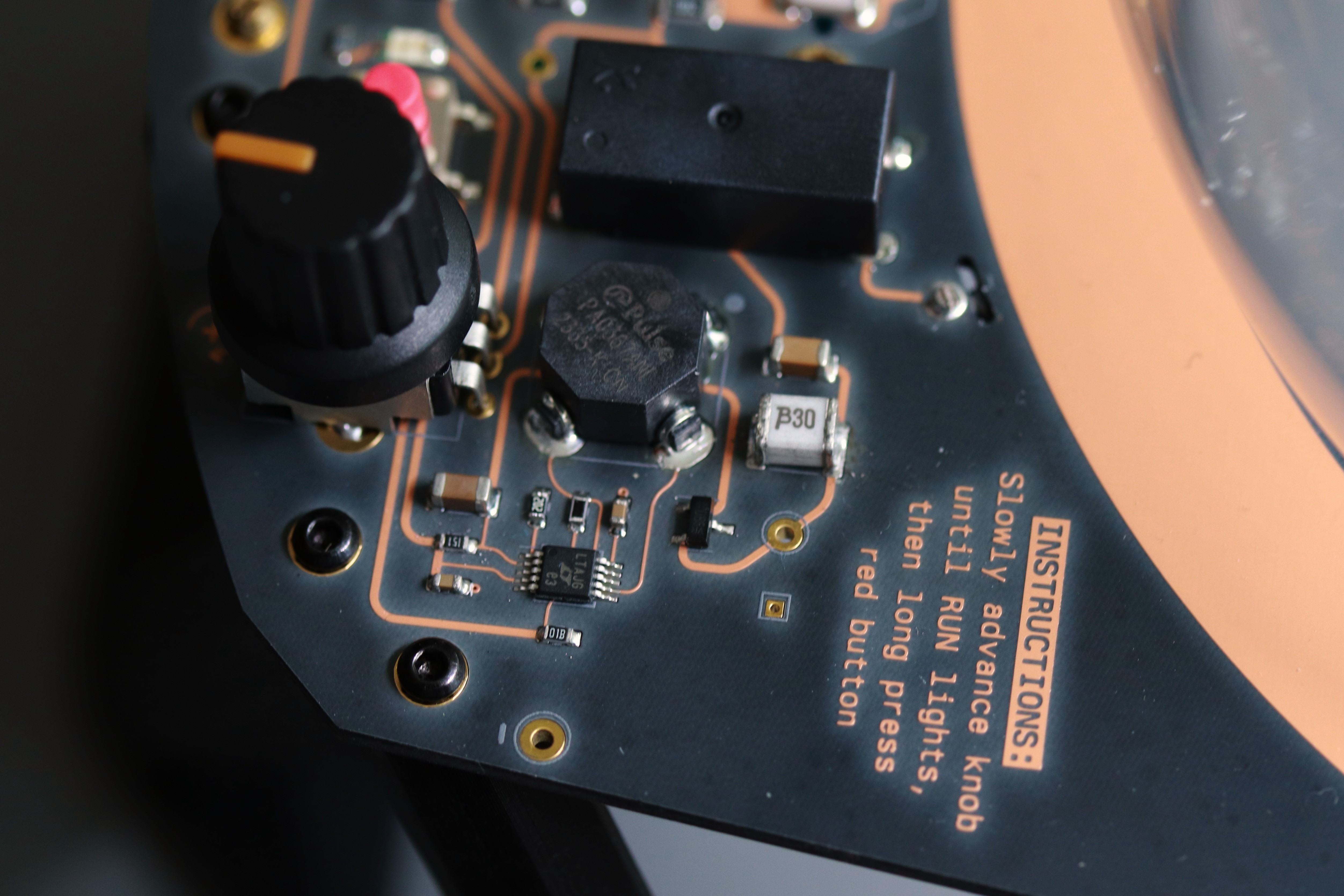
Typical PCBs use a olive-green fiberglass core, layers of copper, and a (traditionally green) soldermask layer to protect the copper and define areas where solder/component pads should stick. This board instead has a dyed-black fiberglass core and a transparent soldermask layer. This means that all traces are visible as their natural copper color, which is delightfully high-contrast against the black substrate. Component pads and other areas left uncovered by the transparent mask are plated (ENIG) gold.
This order of circuitboards was (partially) Sponsored by PCBWay! They covered about 60% of the cost of these boards, and I paid the remainder out-of-pocket.
There's very few photos out there of real PCBs made using this stackup, so I'm taking the time to write out a review.
(Transparency: being partially sponsored will likely bias my opinions, but I did also pay enough to feel like I have skin in the game. I have not given PCBWay any editorial control and they will not have seen this review prior to publication. Photos have been lightly post-processed and are broadly representative of how things look irl under good lighting. An order number [visible on the unpopulated board] has been blurred out for privacy.)An in-depth look
This is going to be mostly photos.
Here's how the board looks straight out of the packaging
![]()
That looks really good, yeah??
The copper is a matte tan, not shiny at all. ENIG gold finish looks like it always does, and creates a neat kind of sandy two-tone.
For scale, the smallest traces on this board are 8mil with fairly generous spacing and the finest pitch component is 0.5mm. Components are D2PAK through 0603.![]()
There's a sort of white ghostliness visible around the copper areas -- I'm guessing due to the transparent soldermask being not pressed quite as deep into the fiberglass. Under certain kinds of lighting, a faint weave texture of the fiberglass can be seen.
![]()
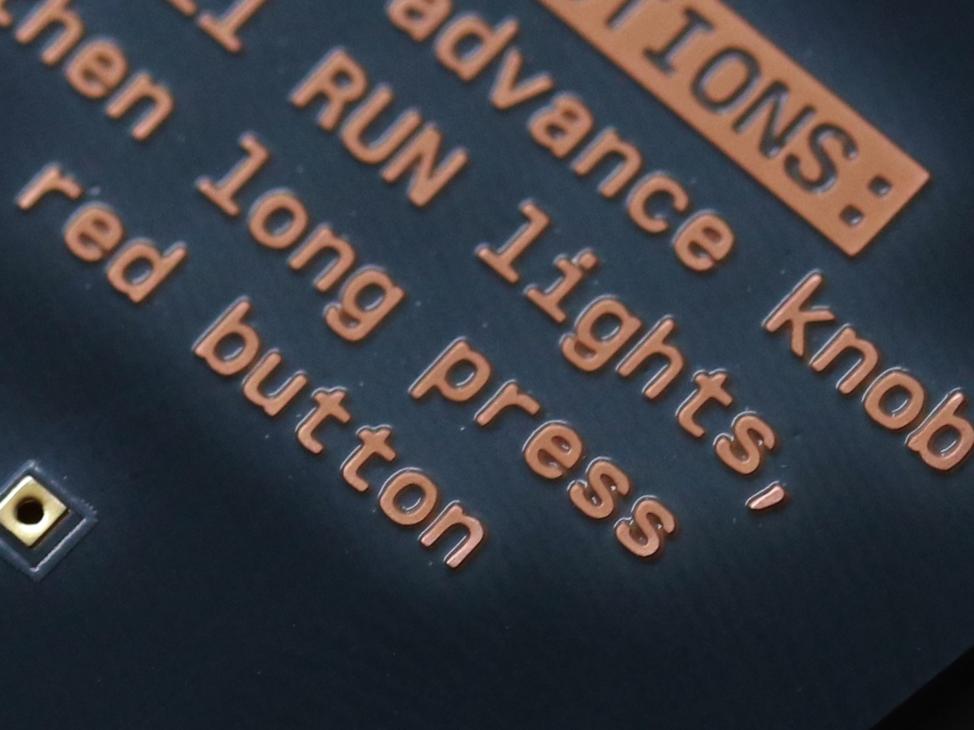
I absolutely love the way that text looks in copper. (This example has a character height of 1.2mm.) Super sharp! There's also a subtle dimensionality visible due to the thickness of the copper and the drape of the overlaying soldermask.
![]()
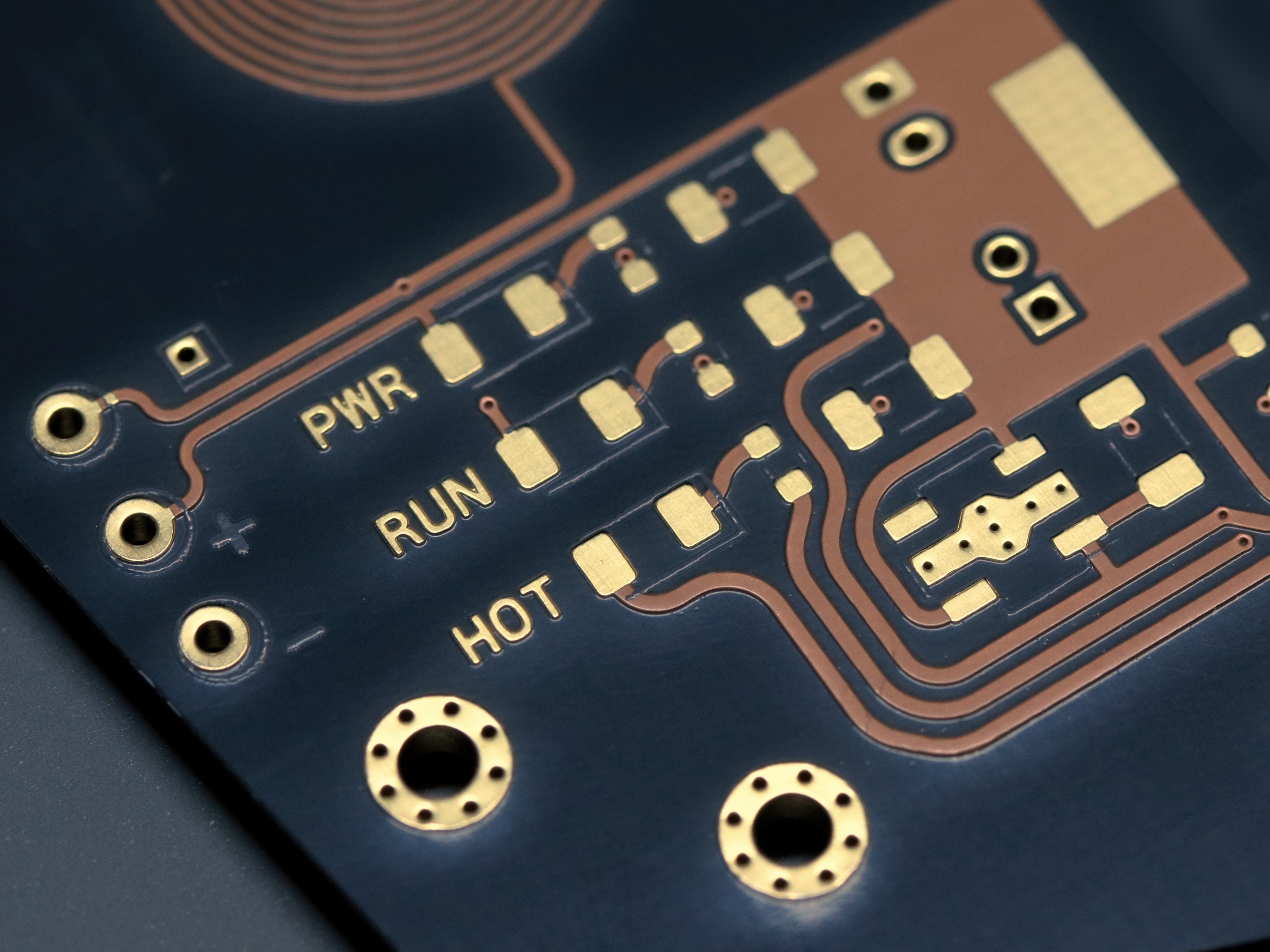
Text in copper+soldermask also looks nice and sharp (although is some slight cruft visible in the notches on the N and W). Contrast is more variable than copper-only as lighting changes, as the gold catches ambient light and reflection differently than the semi-gloss transparent mask.
The grey silkscreen ink is a bit mis-aligned from the other layers. This photo above shows it especially clearly: take a look at the holes on the left side and the silkscreen circles are distinctly off-axis. Silkscreen alignment has been better on my other PCBWay boards, which makes me wonder if the layer required some kind of hand-alignment that's less automated for their higher-order-volume stackups. Not an actual problem but definitely a bit unfortunate.
EDIT, ADDENDUM: My PCBWay sponsorship point-of-contact was perturbed by the soldermask alignment and raised it as a possible issue with their production team. In email correspondence with one of their customer service reps, PCBWay stated that while white silkscreen is aligned by machine, other colors (including grey) are aligned manually and "there will be +/-6mil offset which can not avoid. QC is based on the standard that the silkscreen are not on the pad."
Their Advanced PCB overview lists silkscreen offset as ±2mil, which is presumably representative of their alignment standards for white silkscreen.![]()
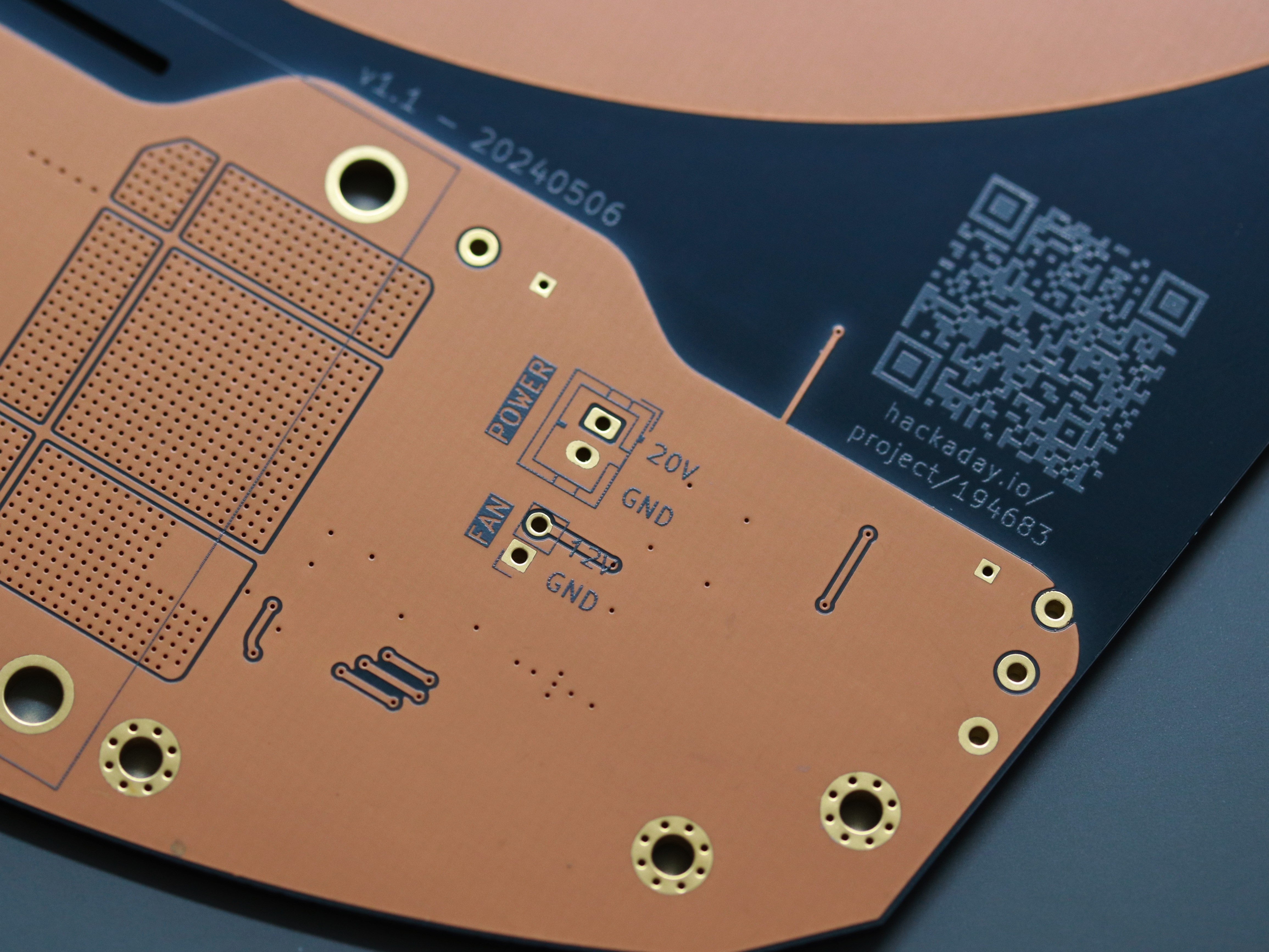
Here's the board backside with its large ground plane. They grey silkscreen QR code is plenty legible against the black FR4. (White silkscreen would be more typical against black, but I thought grey would be a bit more elegant and am happy I made that choice.) The bottom silkscreen is equally mis-aligned as the top.
Grey silkscreen over a copper fill is nice and high-contrast, but readability on the "12V" marking has suffered a lot where I placed text overlapping the edge of a trace.
![]()
An art layer in soldermask on a copper plane also looks pretty good. The "sky-guided, 2024" text is 1mm high and 0.2mm stroke width -- I personally wouldn't go much smaller than that for soldermaskmask graphic strokes over copper. I didn't try gaps in mask over FR-4 because I didn't think it would be usefully contrasting.
Throughout this board, I used the KiCAD plugin "rounded traces" to make the traces curved and flowy rather than angular.
The Cost
Here's the catch though: this board stackup was much more expensive than a standard PCB.
Instead of the quick-turn "Standard" service, getting the black FR4 and transparent soldermask requires the "Advanced PCB" board fab. This run of five 190x145mm boards cost about nine times as much as if I'd purchased a normal stackup (not including the fixed costs of shipping).
As I mentioned up top, sponsorship covered a big chunk of that, but the sponsorship took the order from "nonviable" l;to "still quite expensive". Also as a note, the web order form under-estimated the cost until PCBWay Sales was able to review and give me a final quote. (Their sales team seems distinct from the representative I've been in contact with for sponsorship.)
I suspect that the cost differential would be a lot lower had I been ordering 50,000 boards (or maybe even just fifty) instead of a mere five. I don't have insight into what that pricing might look like.
I also don't know how the costs would change for a much smaller board area.
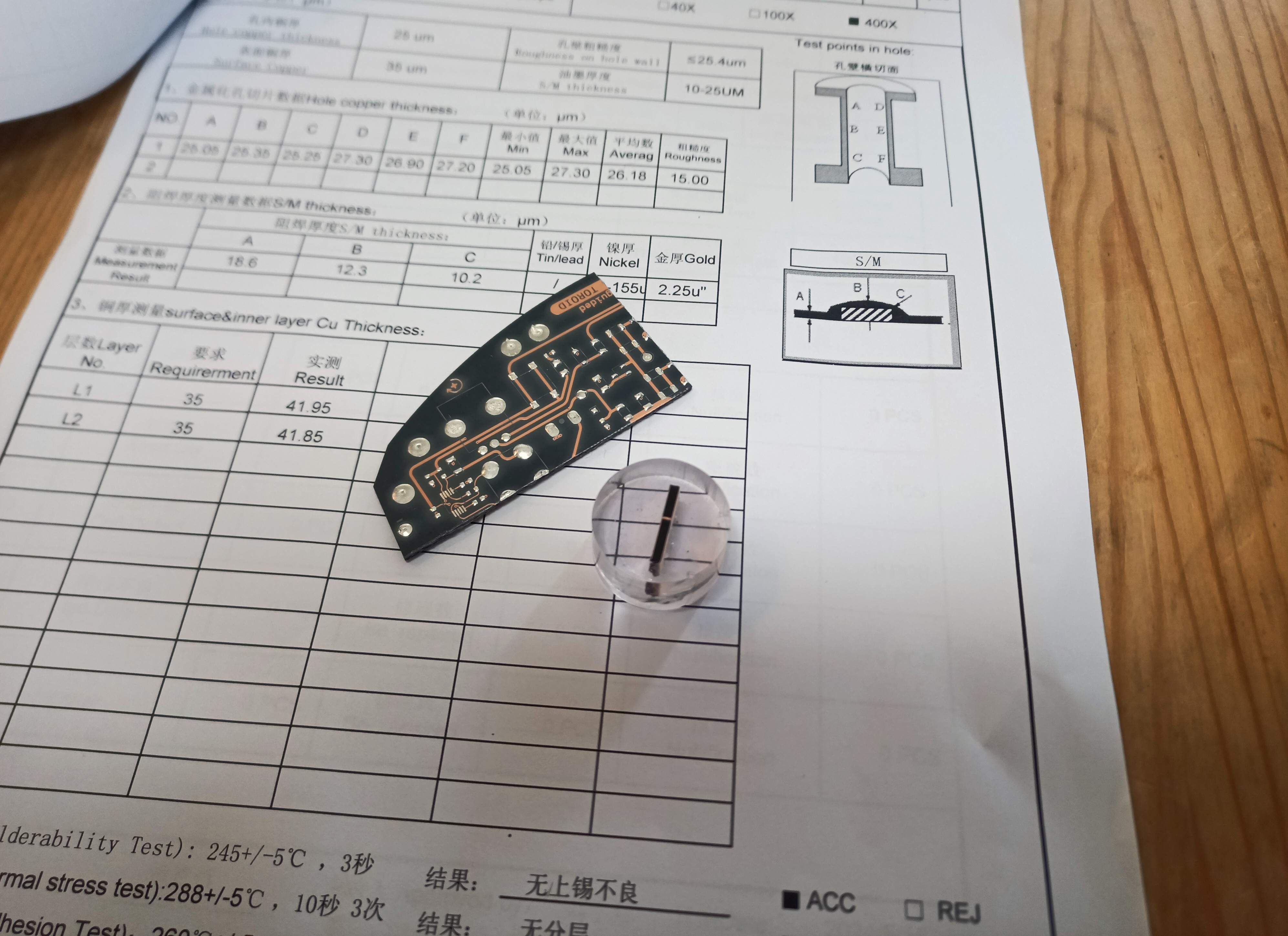
PCBWay sent a full test report for the board -- the "send me a test report" boxes on the order page were checked by default, and un-checking them didn't change the initial cost estimate so I figured why not.![]()
Here's just one page of the extensive test report, plus the two included section boards,one of which was a slice embedded in resin! Quite honestly I didn't need any of that testing -- this board isn't even high-speed enough to be impedance control. I think this is all standard practice for the "advanced" fab service.
Which all raises the very important question: as currently priced,Who is this stackup meant for?
If I'm correct that the cost differential would be a lot less with a large-volume order, that suggests a commercial client might find this stackup a lot more worthwhile. However, I don't imagine there's not a lot of production-quantity products which would benefit from a highly ✨aesthetic✨ PCBs. Enthusiast computer motherboards, maybe? But in most cases, I doubt companies would want to pay even a modest premium for this kind of prettier board.
And on the other hand, I can see a lot of hobbyists who would be super-excited to have a project board (or limited-market production run) looking this swag, but for whom the high cost is totally prohibitive. I would be willing to pay maybe 3-4 times as much for this stackup in select projects, but not 9x as much.
Perhaps this kind of pricing would be fine for convention badge PCBs, which could make use of the unique look while also being both physically smaller and ordered in large enough quantity to offset setup cost.The tooltip for the Black FR-4 option on the PCBWay order page suggests the opacity could be useful for some LED applications, but that seems a separate concern from buying black FR4 + transparent mask for visual appeal.
US-based PCB fabricator OSHpark also sells this stackup (under the delightful name "OSHpark After Dark"), but their per-square-inch pricing model would have made a board as large as mine even more expensive. They're also slower. If your board is a lot smaller, you might consider them as an option.Final Thoughts
I absolutely love the way this board looks, and I'm glad I'm able to use it for my project.
I also wish it were more accessible for other hobbyists. My hope is that PCBWay could figure out a way to get this stackup out of the super-bespoke Advanced PCB production pipeline, since a lot of that functionality is completely tangential to "pcb looks really neat". My suspicion is right now there's the catch-22 of it's too expensive for folks to order, and lack of orders makes it stay an expensive specialty product. Perhaps some kind of special promotion could break the deadlock?
I should also emphasize, these thoughts on pricing are based on the pretty limited sample of this specific large, prototype-quantity board. If that pricing is wildly anomalous, then these hot takes are probably off-base.To wrap things up, here's one more photo:
![]()
Being hyper-conscious of "I want to make this board look exceptionally good" did make laying out and routing the PCB take much longer than it would have otherwise.
I'm happy I took the time to do so. It does look exceptionally good!
Coming in the next update: project showcase, wrap-up, source files, and thoughts for anyone looking to make a toroid of their own. -
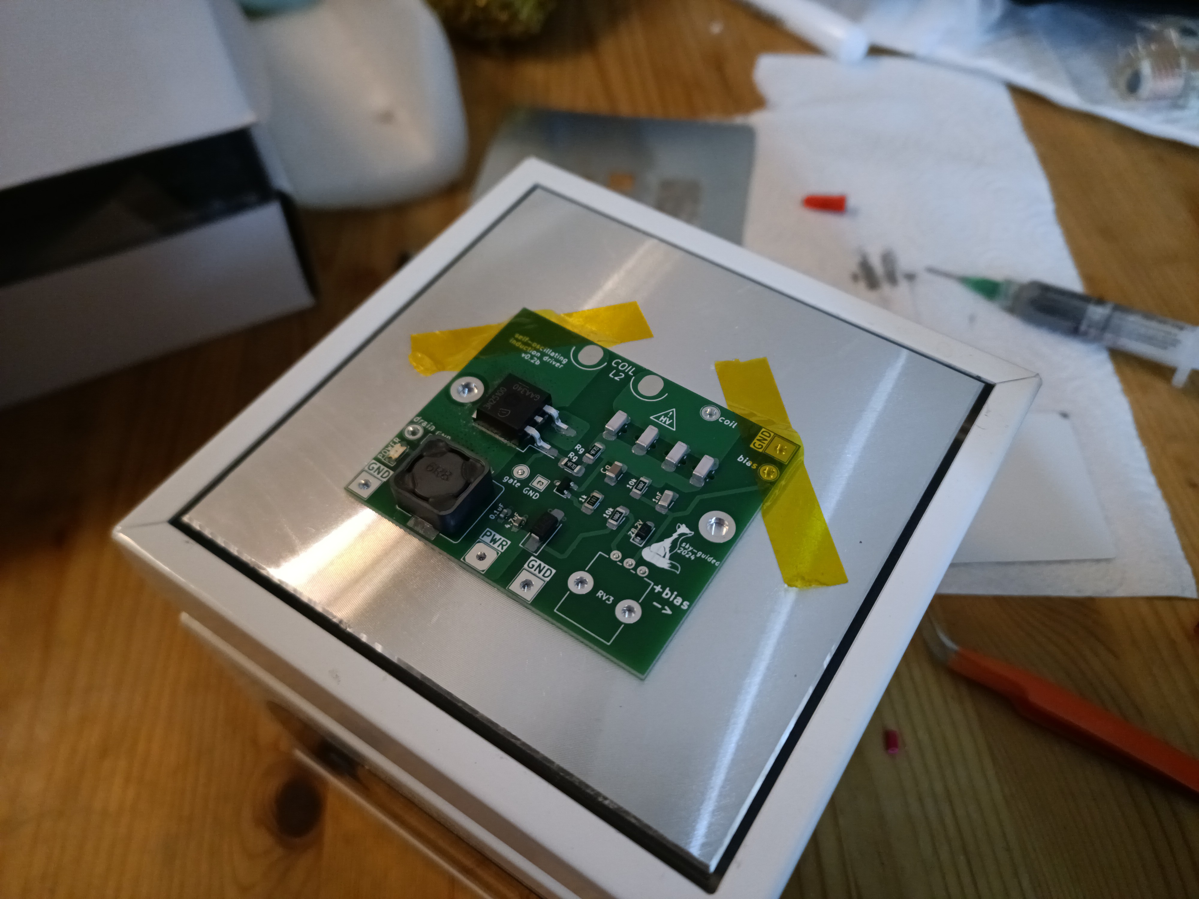
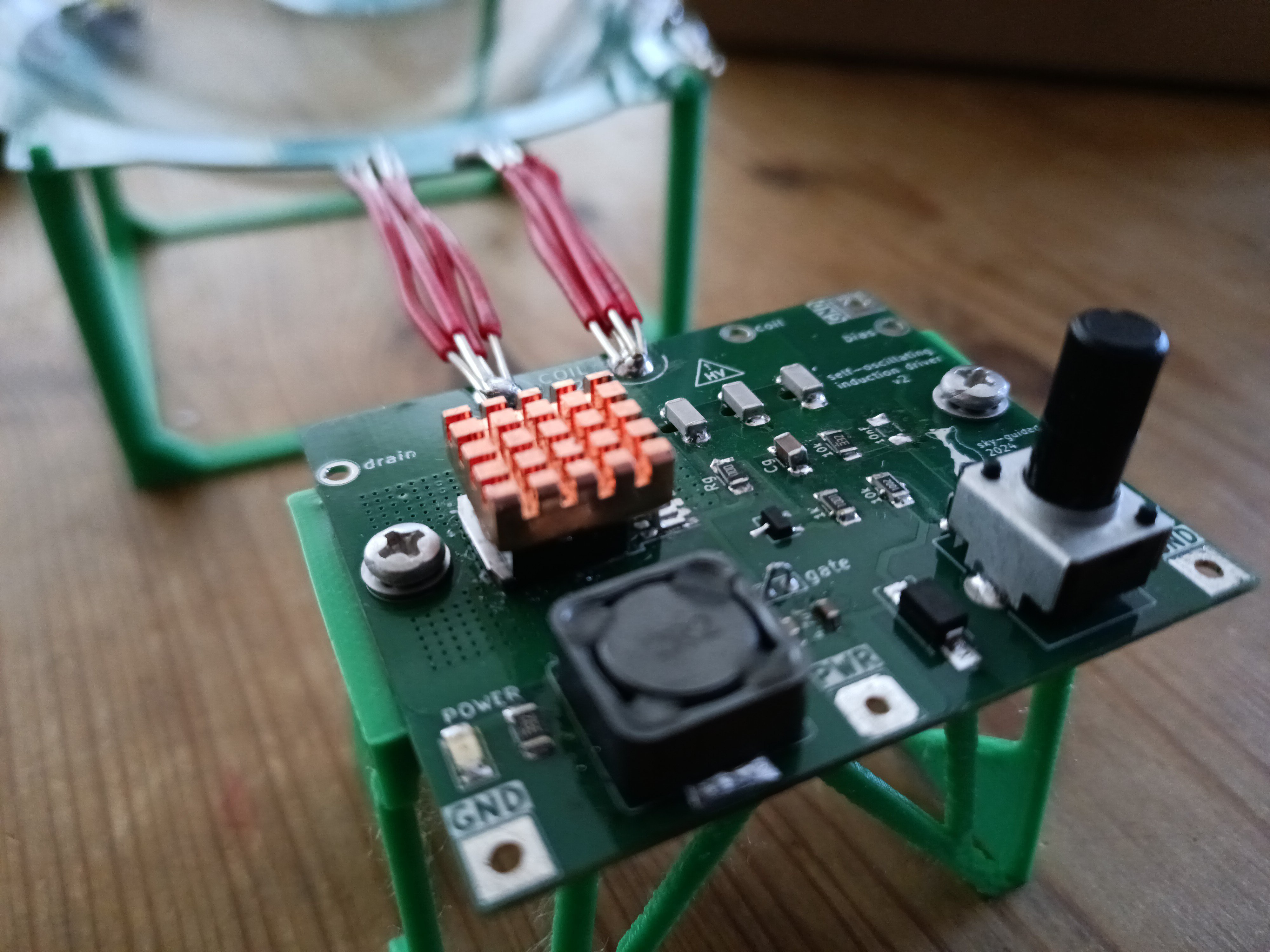
#8: A Unified Board
05/27/2024 at 18:08 • 3 commentsIt's been a busy couple of months behind the scenes -- this project is basically finished! I'll be breaking the final few updates into a couple posts, while I wrangle loans of camera equipment for the beauty shots.
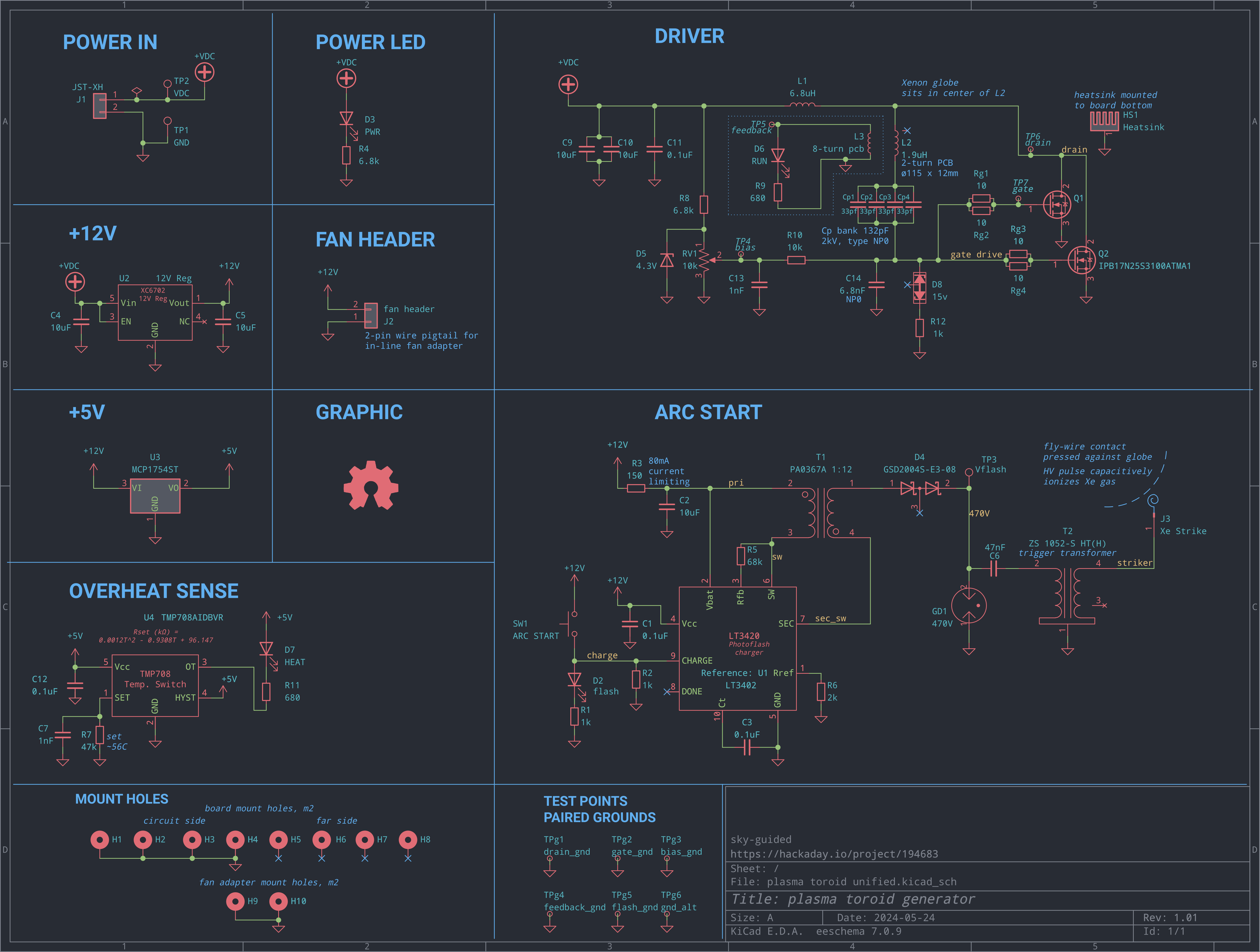
Circuit Unification
Taking the different prototyped modules and banging them together:
![]()
(you might have to click to embiggen)
I've paralled the mosfets for better heat dissipation. This doesn't help quite as much as one would like (since a lot of the losses are switching and not resistive), but it does help. The mosfet gate resistors are also paralled since they get quite hot before the arc is struck. I'm not sure why that behavior is occurring -- if you know, drop me a line!
The 4.3V zener diode (D5) for regulating gate bias is a carefully chosen value for this particular mosfet and circuit. Cranking the knob full-clockwise guarantees oscillations start, but doesn't set the bias so high as to cause excessive power draw and heating. The use of full knob range also makes adjustments more precise and controllable.A bank of four 33pF capacitors is a balance between heat distribution and board space. While the board itself has plenty of room (see below), I ran into some odd layout constraints due to things like the under-board heatsink mounting holes. The cabs do get pretty hot before the arc is struck, but are plenty cool during operation.
There's a total input bulk capacitance of 30μF (shown as two caps on main power and one before the 12V regulator). Less bulk capacitance caused occasional power supply brownout/shutdown.
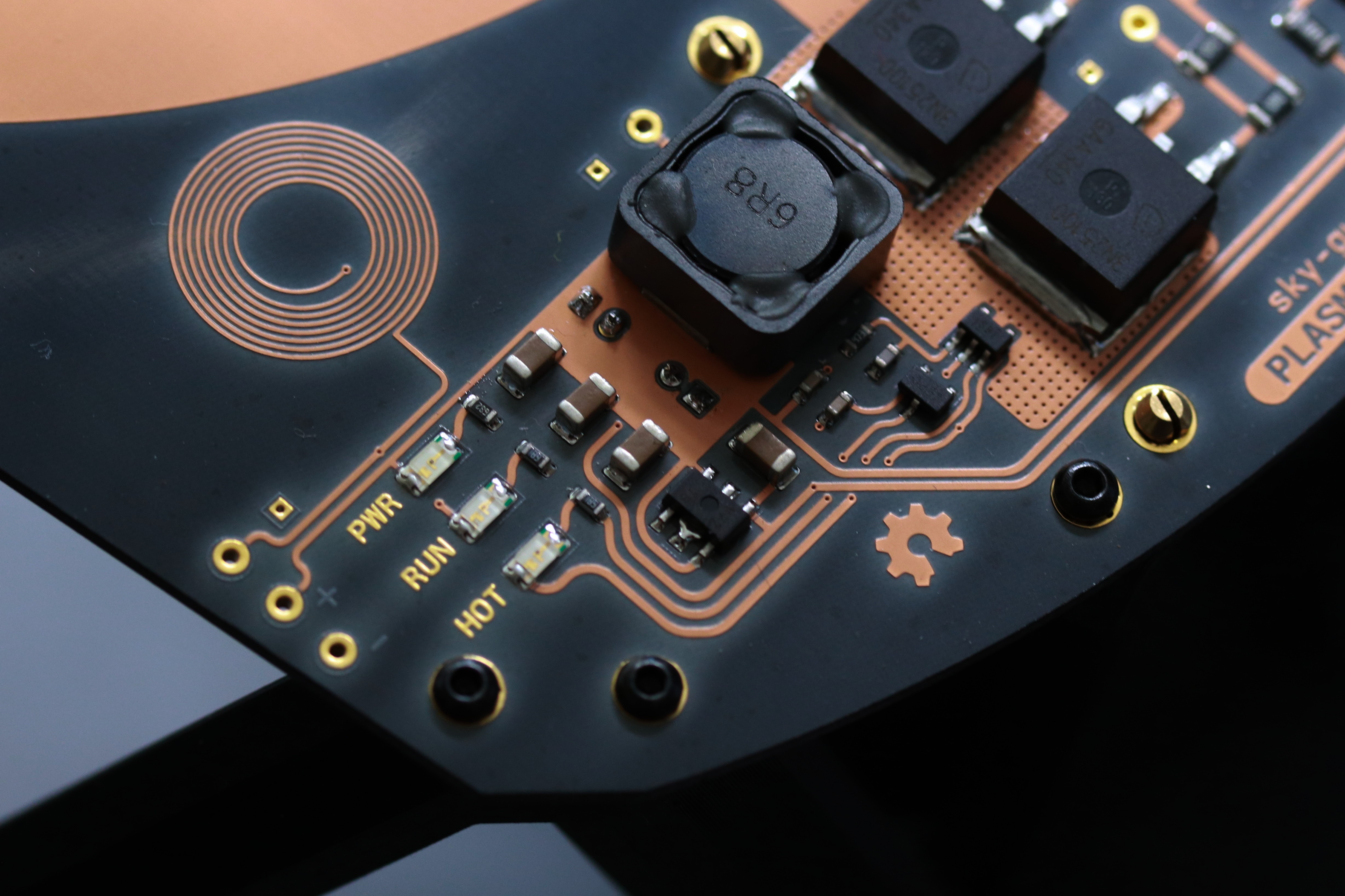
The oscillation sense coil from Update #6 has been brought on-board, shown in the dotted area within the main driver section.
Arc start is basically the same as discussed in Update #7. I keep waffling on whether a GDT value of 300V or 470V is preferable here -- 470V may be shown, but keep your mind open.
The only real new addition is the overheat sense. There's nothing special here; it's almost exactly per the datasheet for the TMP708 IC. The one bit of oddness was having to add a small decoupling capacitor in parallel with the programming resistor, because the overheat IC was placed as close as possible to the mosfet drains and it was picking up EMI. Debugging that was fun -- while poking around with scope probes, I noticed that merely touching the sense pin fixed the problem.
Here's a delightfully goofy photo from a prototype board, showing a 0603 capacitor bodged directly on to the IC pins:![]()
Programming a trip value of ~56C was about right for raising alarm when the mosfet case temperature hit 100C.
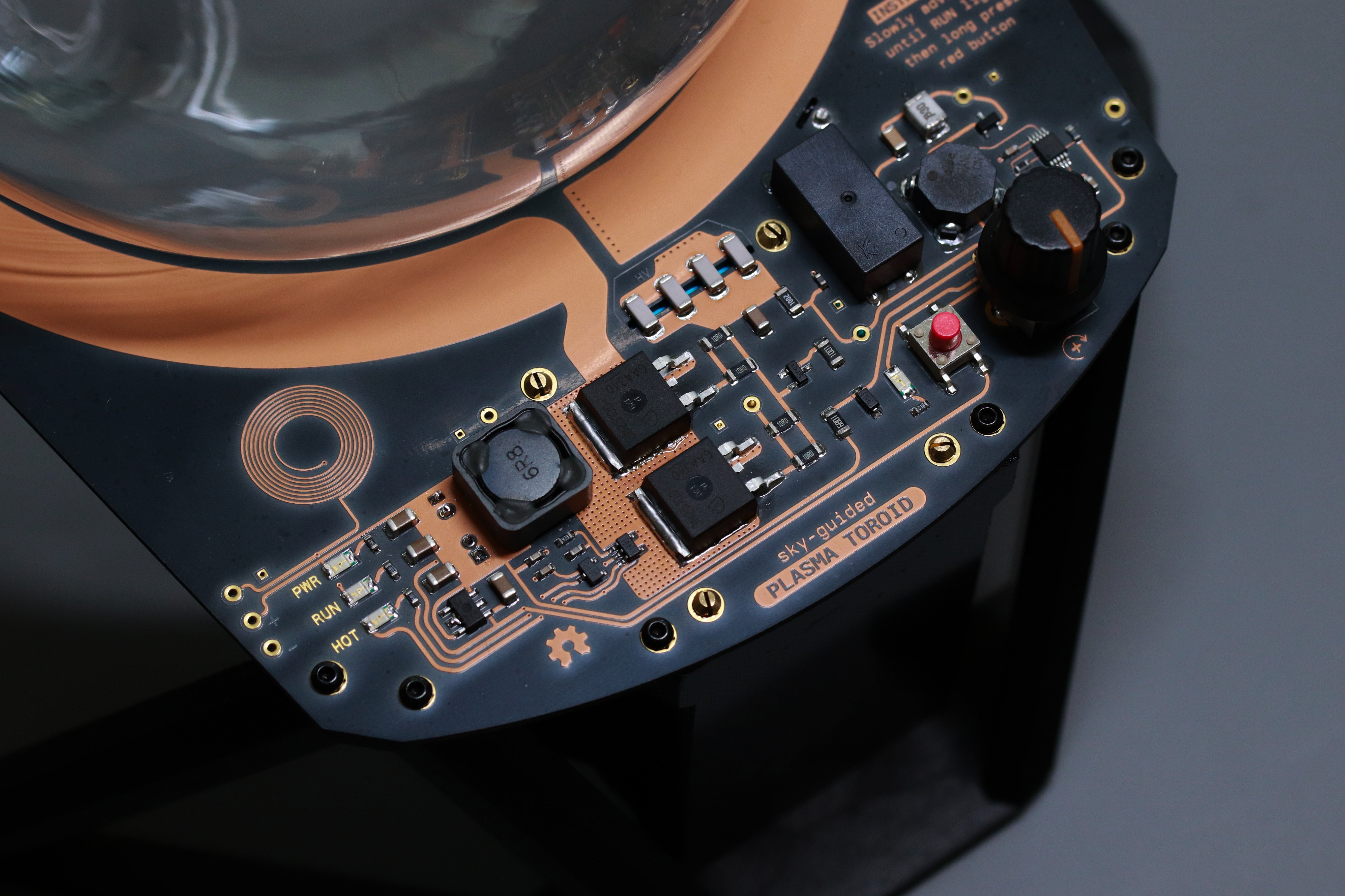
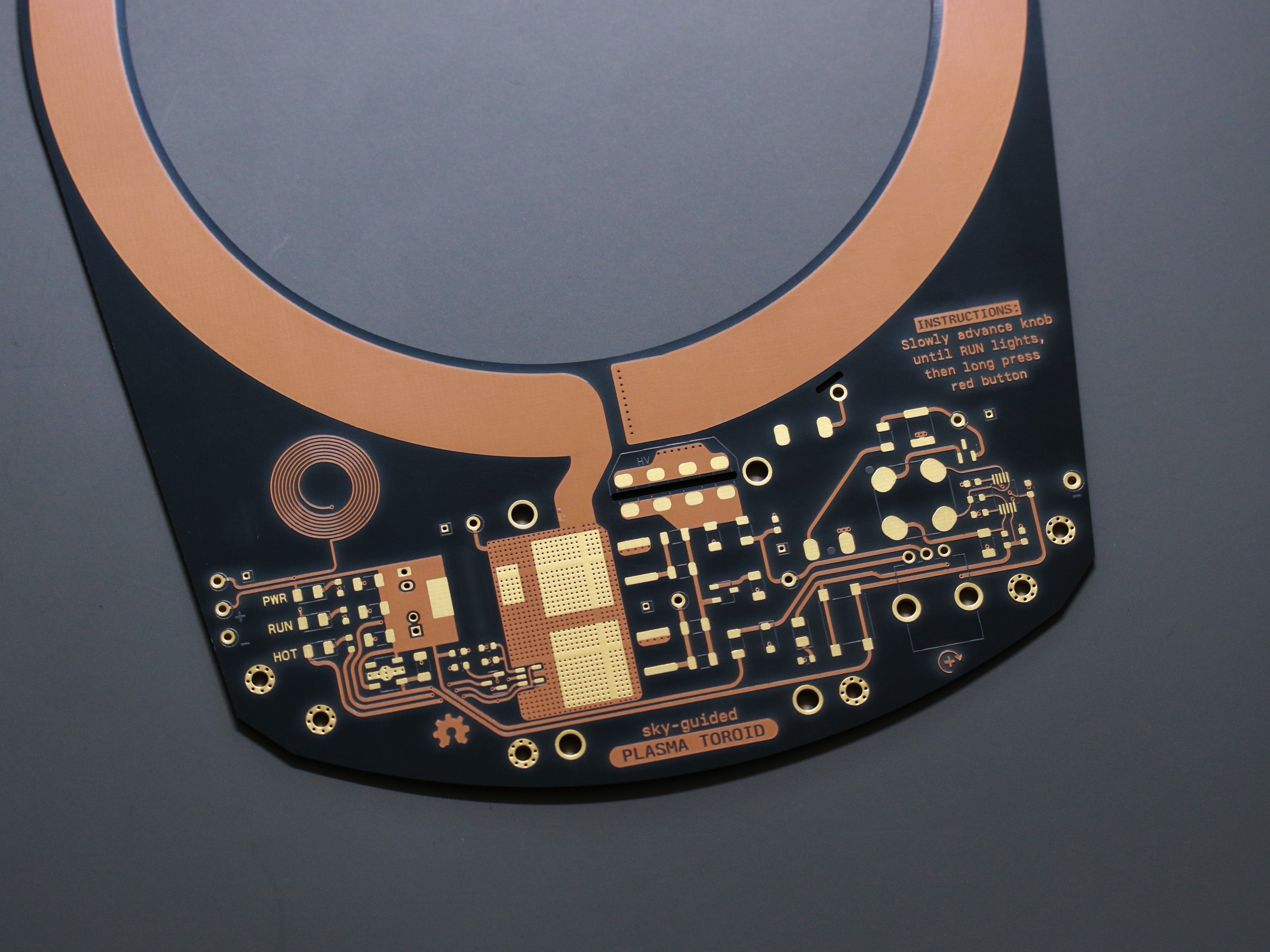
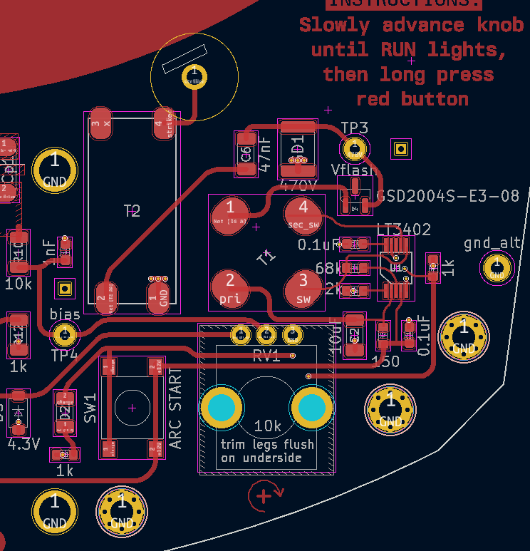
PCB Design
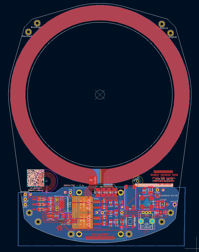
An overview:
![]()
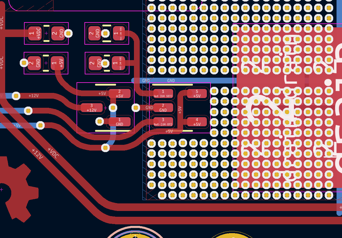
Details might not be super visible at this far out a zoom, but here's the overall layout. Power input and status LEDs are far left, overheat sense is lower center-left, main driver is center (with knob lower center-right), and arc start is far right. The heatsink is mounted to the board bottom, outline indicated by the cyan square around the center area.
Most of this layout is relatively low-density. The minimum size was constrained by needing to fit a heatsink underneath which could accomodate a 40mm fan. There's a handful of components which are 1206-sized even though 0603 would have worked, simply because that larger size looked better.
The rounded traces were made using the KiCAD plugin "round traces".
MOSFETS were placed on a large copper fill, stitched to the heatsink on the bottom with a lot of thermal vias. The thermal tab on the mosfet is attached to Drain (and not GND), so rather than having truly a massive cut in my backside ground plane for the backside Drain copper pours, I split the drain pours into smaller sections with cruciform GND traces.
The TMP708 overheat sense IC was put within a small cutout on the thermal fills, to maximize thermal coupling. A SMD thermal jumper would have been "better" but I didn't want to add it to the BoM.![]()
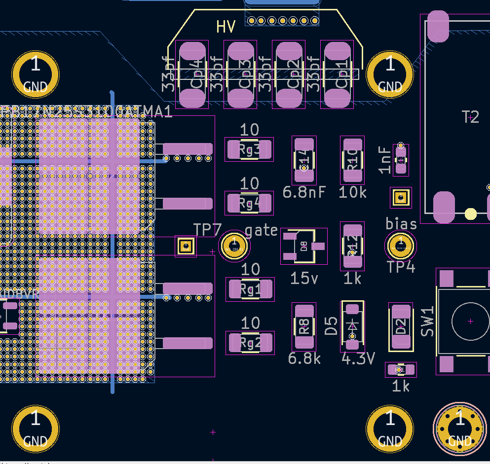
The main driver section in the board center is arranged to prioritize visual symmetry. One detail here is that each test point has a paired ground point to make probing easier. (This project is really sensitive to interference from large loop areas on probe leads!)
A cutout under the primary capacitor bank isn't directly for high-voltage creepage/clearance reasons, but mostly to allow for picking up any excess solder balls or flux residue and is recommended by TDK as best-practice for higher voltage SMD caps.![]()
The far right side of the board hosts the arc-start portion of the circuit. It's mostly notable because I didn't give quite enough clearance for the high-voltage arc start fly-wire contact (J1, visible inside the yellow circle near the top). It's prone to arcing over to the primary inductor. I don't think that's going to hurt anything but it doesn't feel great -- conformal coating or a dab of hot glue might help.
![]()
I am going to open-source this project as soon as I finish this round of update blogs.
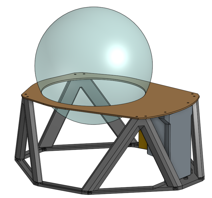
Physical Design
Since the start, a key goal was to have a finished product that didn't look like a workbench prototype.
Here's what I came up with:![]()
Rather than the "layer cake" of most folk's designs, I'm going for something more reminiscent of early 20th century engineering.
Early drafts included a lasercut or printed no-finger-poking safety shield over the electronics, but I decided it looked terrible. Please don't touch the zappy parts.
Components are printed as individual flat pieces, and attached together with heat-press inserts and M2 screws. While a single-piece print would be possible, using multiple parts allows stronger layer-line orientation and avoids print head jump moves which can visibly affect surface quality.
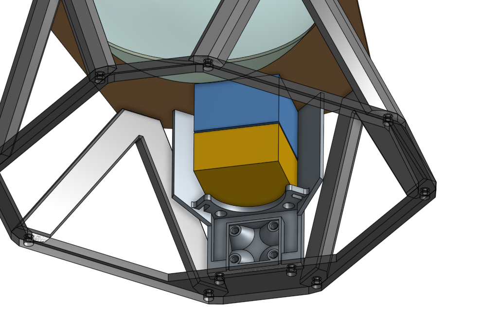
The blocky section in the front-right is a shroud to cover the heatsink (mocked up in blue), and an attachment point for the (brown) 40mm fan. The USB-C power supply module screws down to two of the four semi-conical mounting points.![]()
While I'd have preferred to have the USB-C-PD power supply integrated on to the main board, availability for USB-C-PD trigger ICs in the is currently terrible within the United States. I've decided to use the Adafruit HSUSB238 power delivery dummy breakout as a standalone module. It's a touch larger than some others out there, but it has mounting holes. A standalone board does allow plugging a USB cable in at closer to desk surface height, which in my opinion is a bit nicer.Coming in the next update: an excessively fancy circuitboard, sponsored by PCBWay.
-
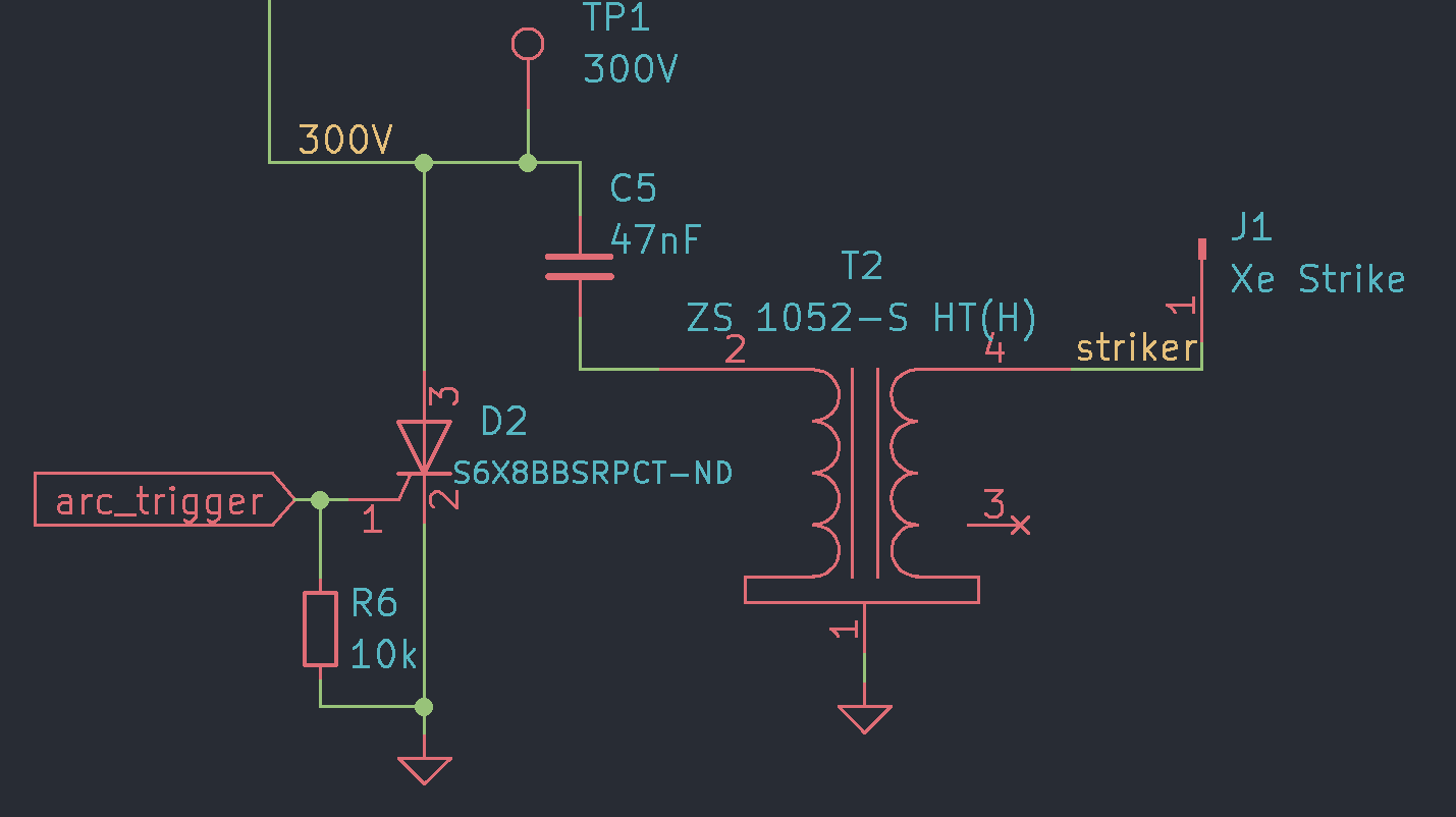
#7: how to ionize xenon: the arc start module
03/23/2024 at 19:24 • 0 commentsThe electromagnetic fields generated primary inductor aren't strong enough to ionize neutral xenon gas into plasma. Once any infinitesimal part of the gas is ionized, those charged particles almost instantaneously cascade into their neighbors and the whole globe lights up. But getting a bit of gas to ionize in the first place is the tricky part.
The "standard" way to do this (as demonstrated by BacMacSci) is to forcefully twist the glass globe against the induction coil. The triboelectric effect causes miniature "static electricity" shocks which are enough to kick off ionization. Alternately, one can use some kind of external high voltage source like a handheld tesla coil zappy gun.
Either manually twisting the globe or using an external device is a bit dissatisfying to me. I wanted to integrate arc start directly into the device, activated by the push of a button.
This log is going to be longer than most, because it's been an adventure.---------- more ----------An external zap?
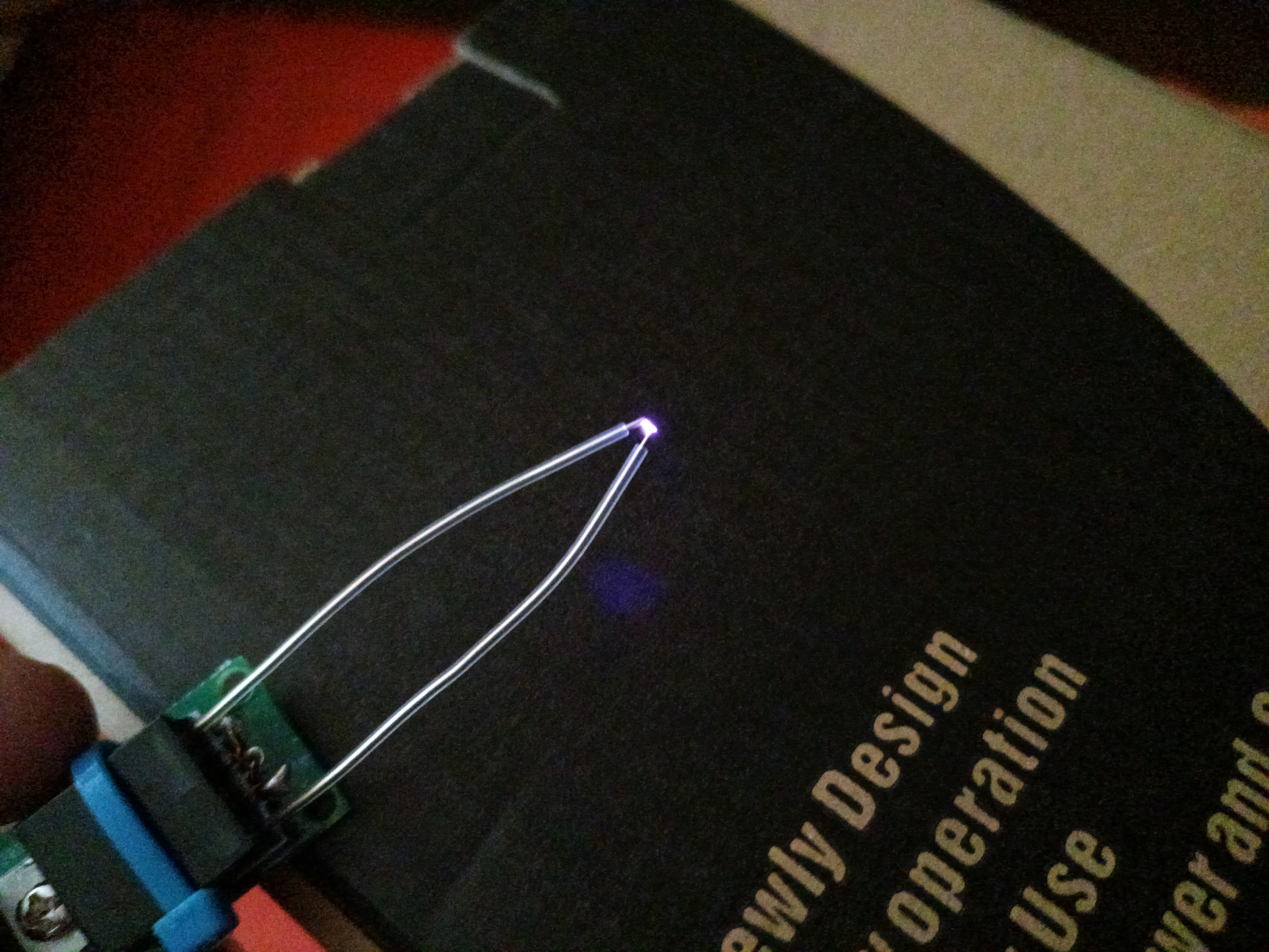
My first attempts were using cheapo "arc lighter ignition modules" sold on aliexpress or amazon. (I won't bother linking, because those listings seem to have a half-life of like six months and dead links suck.)
![]()
zap
BigCliveDotCom has a great video explanation into how this circuit works. I think it could be best described as "aggressively cost-optimized.
Holding the contacts against the globe could occasionally start ionization, but that was rare. Most of the time it did nothing, regardless of positioning.
This was a dead end.
So I thought, well, xenon flash tubes for cameras and strobe lights and stuff exist. How do those work?Triggering xenon flash lamps
BigCliveDotCom also has a video on how xenon flash lamps are fired, titled "Unwinding a tiny 6kV xenon trigger transformer". He's phenomenal at concise explanations of how circuits work and this is no exception -- I'm going to embed it here, because his description is better than what I can muster. The circuit diagram and explanation is from about 1:53 to 4:30
The shortest version is that a small capacitor is charged to the neighborhood of 300V, then rapidly discharged through the primary of a high-turns-ratio transformer. This creates a very high voltage pulse on the transformer secondary, which is fed to a fine wire wrapped around the glass of the xenon flash tube. The high voltage causes capacitive coupling to the xenon through the dielectric of the glass, strong enough for ionization.
Here's my implementation:![]()
It's the same circuit BigClive drew. No magic here.
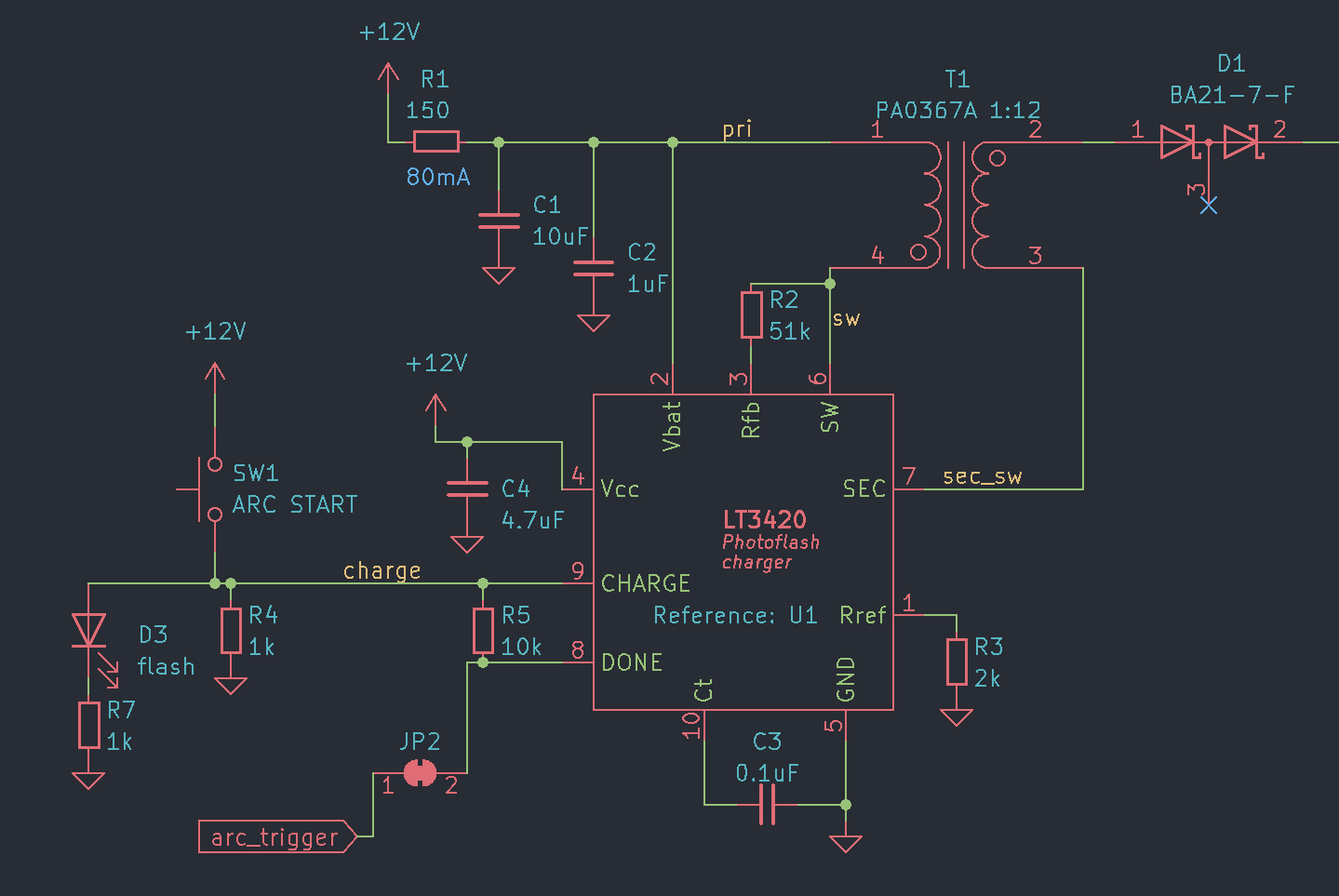
Component D2 is a thyristor, an old-school cousin of the BJT. When a voltage is applied at the gate it latches closed until current flow drops below a low threshold value.Getting 300 volts
There's lots of ways to get 300-ish volts from low-voltage DC, and most of them are some variant of flyback converter.
Properly engineering a flyback converter is a bit of a rabbit-hole, and these days it seems like most commercial applications are in low-volt-dc switch-mode power supplies. I decided to take the shortcut of using the LT3420, an IC purpose-built for charging photoflash capacitors.![]()
This is very nearly the same circuit as the reference design in the datasheet. I'm even using the same flyback transformer that they recommended. (That's one thing I love about hobby electronics -- device manufacturers actively do what they can to make implementation of their parts as easy as possible.)
There's a couple of deviations from reference, though. R1 is a current limiting resistor; since I'm only charging the teeny 47nF trigger capacitor and not a larger flashtube cap, I can store the needed energy in a "slow"-charged onboard 10uF cap rather than the transformer drawing directly from the 12V rail (and correspondingly needing a 12V regulator with a higher current rating).
The DONE pin goes high when the IC thinks that the transformer output has been charged to the nominal voltage. My design intent here was to use this signal to automatically fire the triggering thyristor when the threshold was reached. Normally DONE has a pullup, but I decided to get overly clever and pull it up to the CHARGE line so that in theory it could only go high when the arc start button is pressed.JP2 is a cuttable jumper trace, since I figured that I might have issues with thyristor trigger reliability and need to try external trigger signals. This ended up being a prudent bit of defensive design.
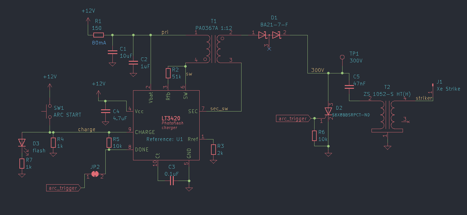
Putting the 300V charger and the trigger circuit together, here's what we get:
![]()
A downside to this approach is parts availability and cost. Xenon flashtubes for photos have fallen out of favor so these have become "specialty components". In particular, the LT3420 costs like $8 each, and the transformers together are about $7. That might not seem like much but it adds up when buying prototyping quantities of even just five or ten pieces.
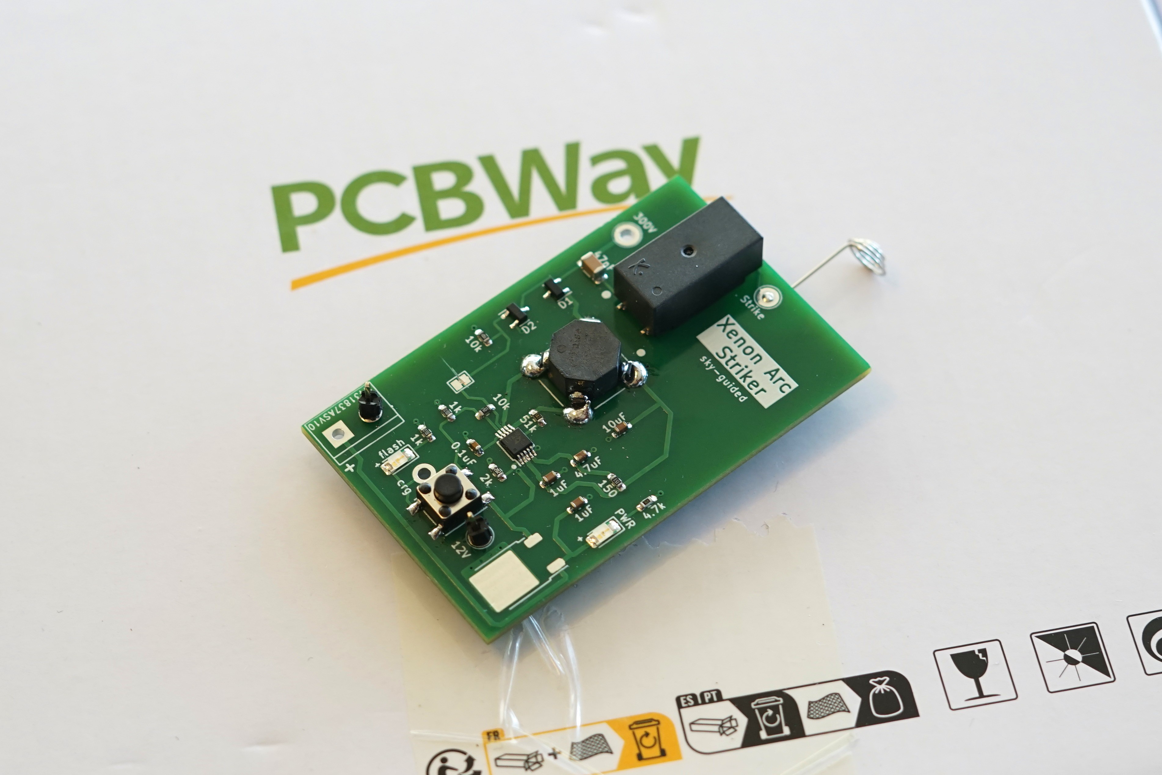
Circuitboard
As previously, this board was sponsored by PCBWay! Their product quality is, as always, solid.
![]()
The actual contact point for the xenon globe is a little spring-steel AAA battery terminal, extending to the upper-right. A little bit of of hand forming is required, but the springy contact is great for gently conforming to the globe's surface. A wire wrapped around a cylindrical flashtube may be traditional, but trying to wrap around a spherical glass vessel is misery.
Unfortunately, I made no less than four different errors when laying out this board:- There was supposed to be a 12V regulator on board, but it's unpopulated (the large footprint at the board's bottom). This was because I made a last-minute decision to swap the regulator I had on order from one with a DPAK footprint to a smaller SOT89, and I neglected to update the layout.
- The Pin 1 marker on the (octagonal) flyback transformer is on the wrong side -- I had primary and secondary backwards. Probably a mistake in the "alternate pin assignments" options in KiCAD.
- The footprint of the flyback transformer is also wrong -- the spacing is too wide. I suspect when laying out the footprint I was entering pad edge-to-edge dimensions as if they were center-to-center.
- The thyristor (D2) had gate and cathode pins swapped. This last was fixable with a bit of bodge wire excellence:
![]()
With the board assembled and the bodges all bodged, did it work?
Well... kinda.
First iteration: almost working, but not quite
The flyback was successfully able to charge the trigger cap up to >300V. Quite a bit higher, in fact -- the voltage was going literally off the scale that my scope would display. The charge control IC should have automatically ceased charging when the output hit a voltage threshold programmed by a feedback resistor, but in practice I think it was charging the 47nF trigger cap fast enough that the IC control got kinda wibbly -- in a usual application it'd have caps which would charge on the order of several seconds, not a few milliseconds.With full charge, I could manually short the high side of the trigger cap to ground, and produce the sharp-edged pulse to drive the trigger coil. Doing this could sometimes cause the xenon globe to ionize, but it was very inconsistent.
Getting the thyristor to switch consistently was a minor ordeal. First there was the aforementioned "gate and cathode were wired backwards" problem. Then there was a bit of a wild goose chase seeing if an external 555 timer circuit could produce more reliable results than the DONE signal from the IC. Eventually I determined that the thryistor could switch just fine when the board was sitting on the bench, but when I tried to actually use it to strike the toroid arc, the driver's primary inductor was causing electromagnetic interference so intense that the thyristor was firing prematurely. Replacing the 10kΩ pulldown resistor with a 1nF bypass capacitor helped a bit, but it was still never able to get the xenon to ionize.
Second iteration
I had to take a step back and ask myself, "what problem am I actually trying to solve here?" The goal was to discharge the capacitor in a sharp pulse when it reached 300-ish volts. A DIAC could do this, but that would be yet another specialty component with terrible selection and availability. Alternately someone named Pagurja has a youtube video titled "The simplest xenon flash circuit" which demonstrates forcing a BJT into avalanche breakdown to create the fast pulse required. This is apparently a secret-sauce way of creating ultra-fast pulses for things like oscilloscope bandwidth characterization, but I wasn't excited by the idea of relying on semiconductors pushed so far outside of their designed and characterised regimes.
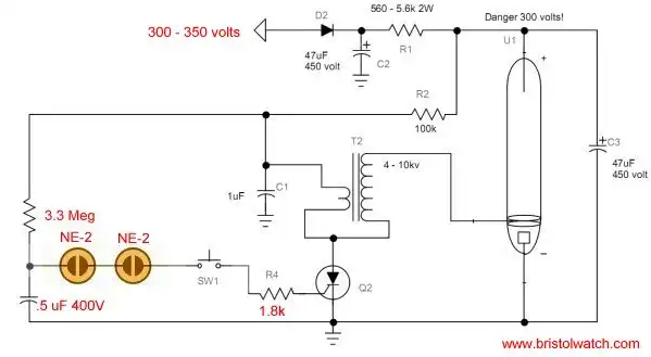
The breakthrough came when I saw this note from Lewis Loflin at bristolwatch.com describing using two ne-2 neon bulbs as part of a trigger circuit.![]()
I figured, heck, why not use some kind of spark gap type thing as the trigger switch itself?
Web searching things like "specific voltage spark gap" etc lead to my discovery of a device called a gas discharge tube arrestors. These little guys are perfect -- it's a sealed tube with some magical gas mix inside, specifically designed to break down and conduct at a particular voltage. GDTs are generally used for circuit protection; they sit at near-infinite resistance unless a high-voltage transient comes down the line, at which point they function as an overvoltage crowbar. They even come in tiny surface-mount packages, at prices of well under a dollar.
I should give specific credit to this 2021 post on the EEVBlog forum from a user named Gyro. They link to a PDF copy electronics hobbyist magazine from way back in 1978, presenting a circuit that's conceptually nearly identical to what I need!
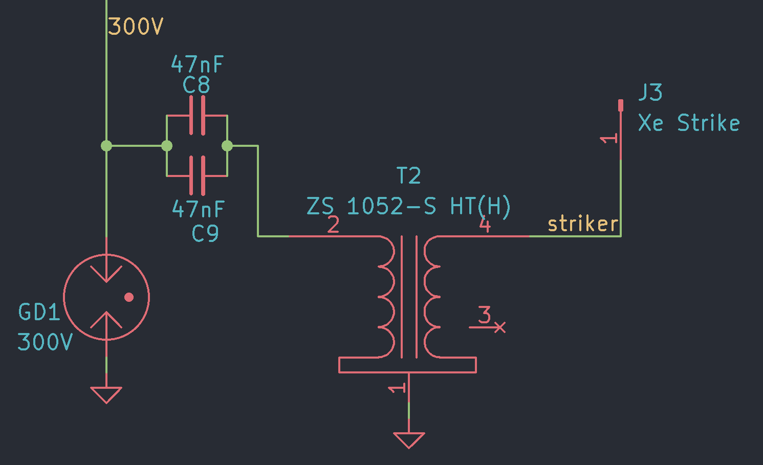
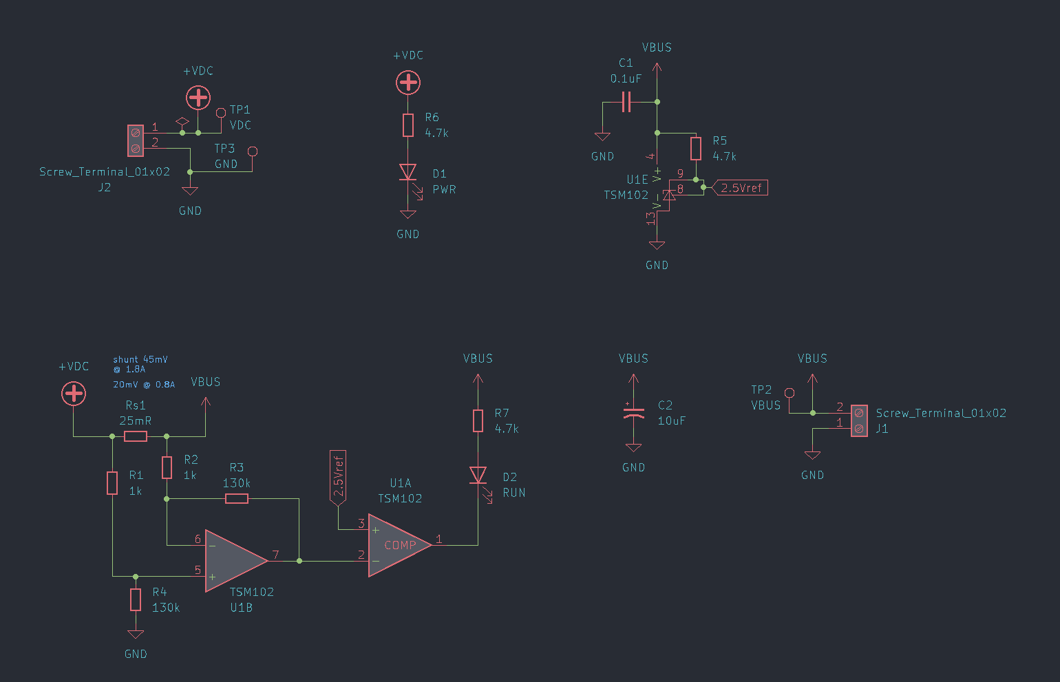
Here's what the revised trigger section looks like:![]()
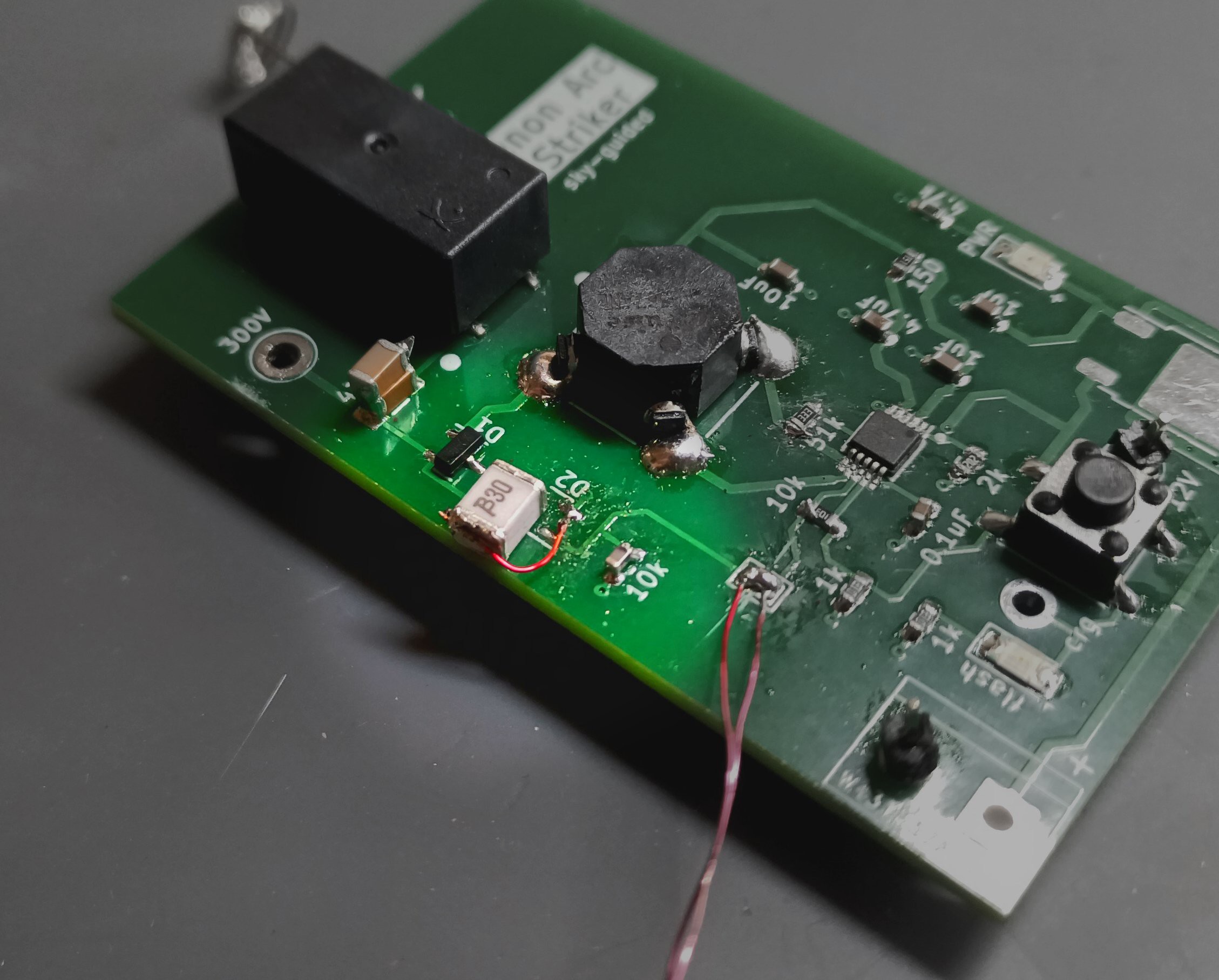
And here's the actual GDT, bodged in to the board in place of the thyristor. It's only a 1812-sized SMD part!
![]()
I double-stacked two of the 47nF capacitors during earlier testing, and didn't feel any strong need to change back to a single cap.
Results
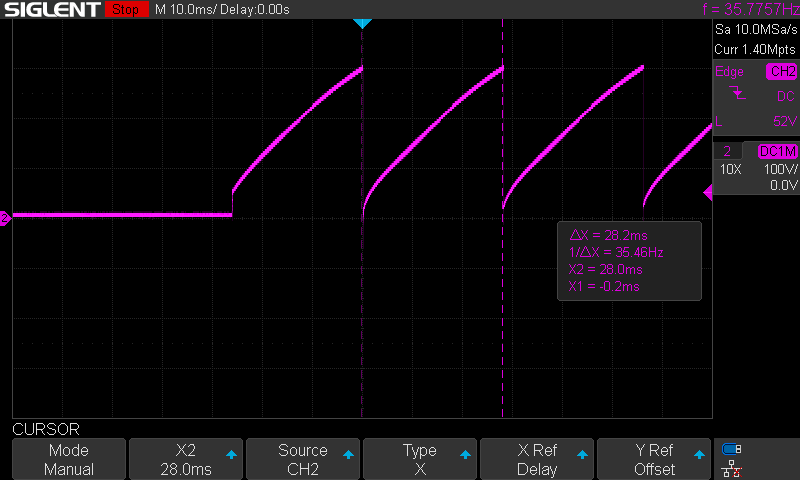
Here's the scope waveform measured at the "300V" test point.![]()
Exactly as intended. The capacitor is charged up by the flyback, then automatically discharges through the GDT when it hits 300 volts. Not pictured here is the corresponding high voltage pulse on the trigger transformer secondary. This happens at a frequency of 35Hz, so you get that nice clicky-buzzy noise reminiscent of a stun gun arc, but much quieter.
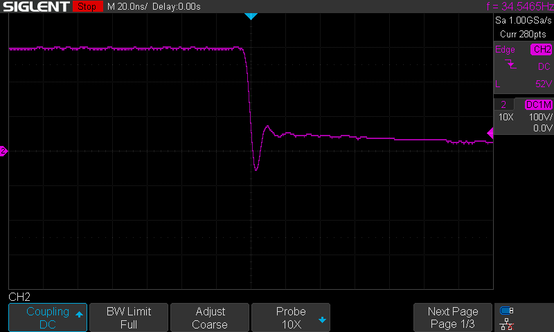
Zooming the timescale wayyyyyy in, here's a single discharge:![]()
The pulse time is under 5ns. Not gonna set any records, but pretty quick.
Video demonstration:As you can see, from a cold turn-on it takes a few bursts of the zappy to get going -- the xenon seems a bit harder to ionize before it warms up. Once the globe is warm, the module can strike an arc almost instantly.
In the final build this module will be integrated as part of the single driver PCB.
WHAT'S NEXT
Getting the arc start module working is a big deal. All of the individual subsystems are functional and core design milestones have been hit:
- Initially achieving the plasma toroid effect.
- Refining the driver to run continuously without melting.
- Tuning a plasma donut that can be either eerily stable, or intriguingly mobile.
- Powering the driver via USB-C (which I haven't yet described, since I'm using an off-the-shelf USB-PD board which Just Works in a delightfully boring way.)
- An indicator light for whether the circuit is in oscillation.
- Pushbutton arc start.
Now I gotta put all the pieces together. I'm certain the result is going to be gorgeous.
See you next time! -
#6: status LED, galaxy brain style
03/22/2024 at 16:20 • 1 commentSince a key goal of this project is to run standalone -- no o-scope, no bench PSU, no amperage panel meter -- it's crucial to have some sort of indication of whether the circuit was in oscillation or just sitting idle.
Overall power draw reliably reflects the circuit's state. When not oscillating, there's near zero draw -- just LEDs, leakages, etc. While running the draw is more like 2-3 amps, and can be reduced down to as little as ~1.2A by lowering mosfet gate bias.
The normal approach
I had initially planned to use the pretty typical current monitoring method of a differential op-amp measuring voltage across a low value shunt resistor. Since I'm looking for a threshold current indicator rather than a continuous analog signal, the op-amp is fed into a comparator, against a reference voltage.
![]()
Yes, this diagram is kind of sloppy, but you won't need to linger on details here anyway. If the text is unreadable due to aliasing you can click to embiggen.
The TSM102 IC seemed like a neat combo-wombo of packaging two comparators, two op-amps, and a 2.5V reference all in one. It's also relatively inexpensive and can run off of a 40V Vcc. Purpose-built current monitor ICs also exist, but I didn't necessarily want to add a 5V regulator just for one chip, plus I thought the extra op-amp/comparator channels might also be useful for other functionality.
As mentioned in the previous project log, PCBWay sent me a sponsored board and solder stencil! Assembly was quick and easy. Thanks, PCBWay!Well?
It didn't work.
Output voltages from the op-amp do move in response to changes in the drive power, but not in any way that's intended. I suspect that the choice of 25mΩ shunt resistor is just way too low for this application, and is getting drowned out by common-mode influences and amplifier limitations. Using 130kΩ resistors as part of the op-amp network was definitely a warning sign that things might be getting a bit too off-road. 45mV seemed an ok enough differential when I thought a 1.8A current threshold would be good, but lowering that threshold down to 800mA / 20mV certainly didn't help. (Or maybe I'm just not very good at this, and there's a fundamental design error that's gone unnoticed.)
That's all ok though, because I had a better idea.---------- more ----------Going Wireless
While testing out the (still-not-yet-documented) arc start module, I had to start up the main driver circuit and decided to not even hook up my scope leads for monitoring, since I figured that the primary inductor oscillation was electromagnetically noisy enough to be perceptible without a direct connection.
And that's when the inspiration hit.
Just by wrapping a clippy test lead into a li'l coil, there was more than enough inductive coupling from the primary to wirelessly light an LED. In fact, this video is of my second test of this method -- the first time I used a raw 5mm LED which burned out within a few minutes from being overdriven. (The LED shown is an "E-Cell" breadboard-friendly LED + resistor, sold by DFrobot. Super handy prototyping aid.)
This video also shows how ghostly the toroid looks with daylight filtering in through living room windows. Very different from the dimmed-room beauty shots!
IMO this monitoring method is better than a fixed yes/no threshold on current draw, since the LED brightness visibly changes in proportion to the drive intensity. It's also a much more direct measurement of what the coil is actually doing.
Feeding an inductive pickup directly into an indicator LED is either the cleverest or the most knucklehead way of solving the status monitoring problem. Probably both at the same time, really.
I can design a PCB coil trace as part of the finalized circuitboard assembly, for zero added cost. That brings the subcircuit component count from ten (including one not-recommended-for-new-designs IC) all the way down to a mere two.
Nice.
Coming next, we finally grapple with push-button arc start. -
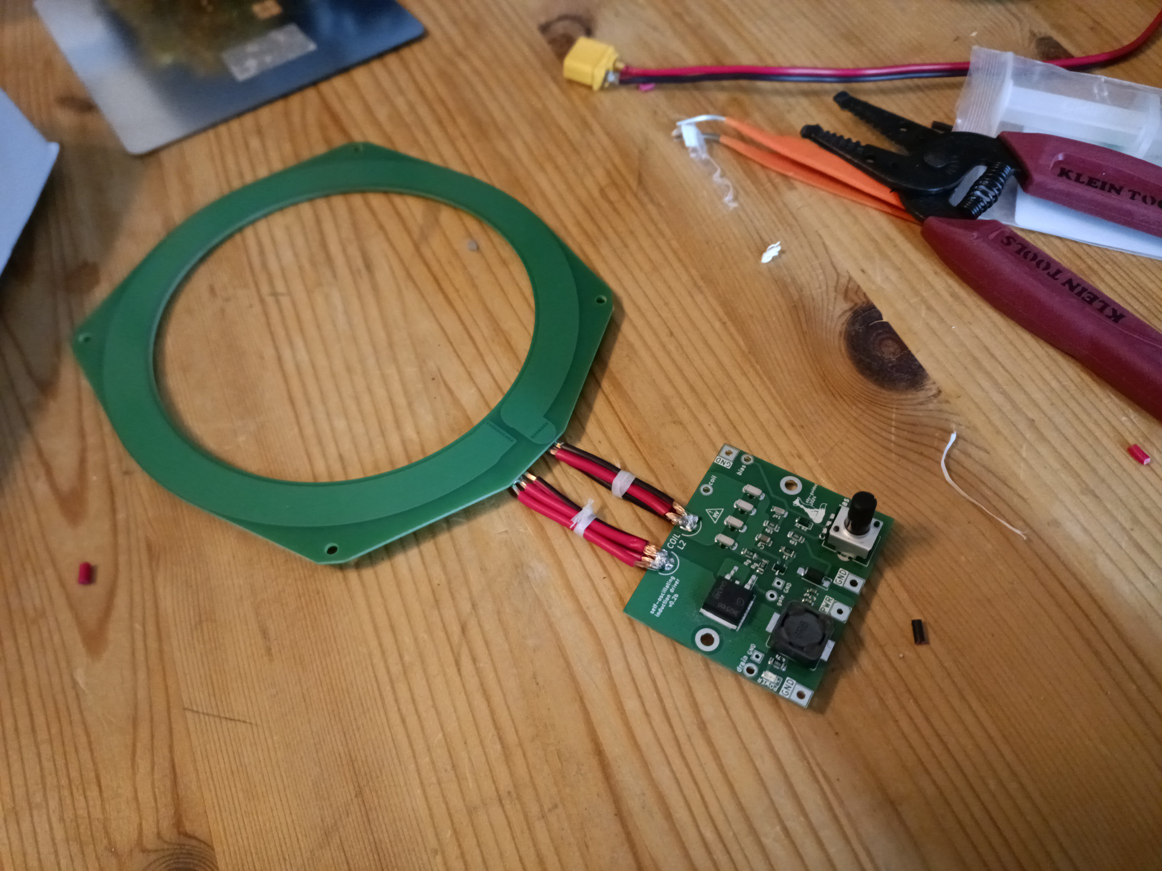
#5: Version 0.3 is calm, cool, and collected
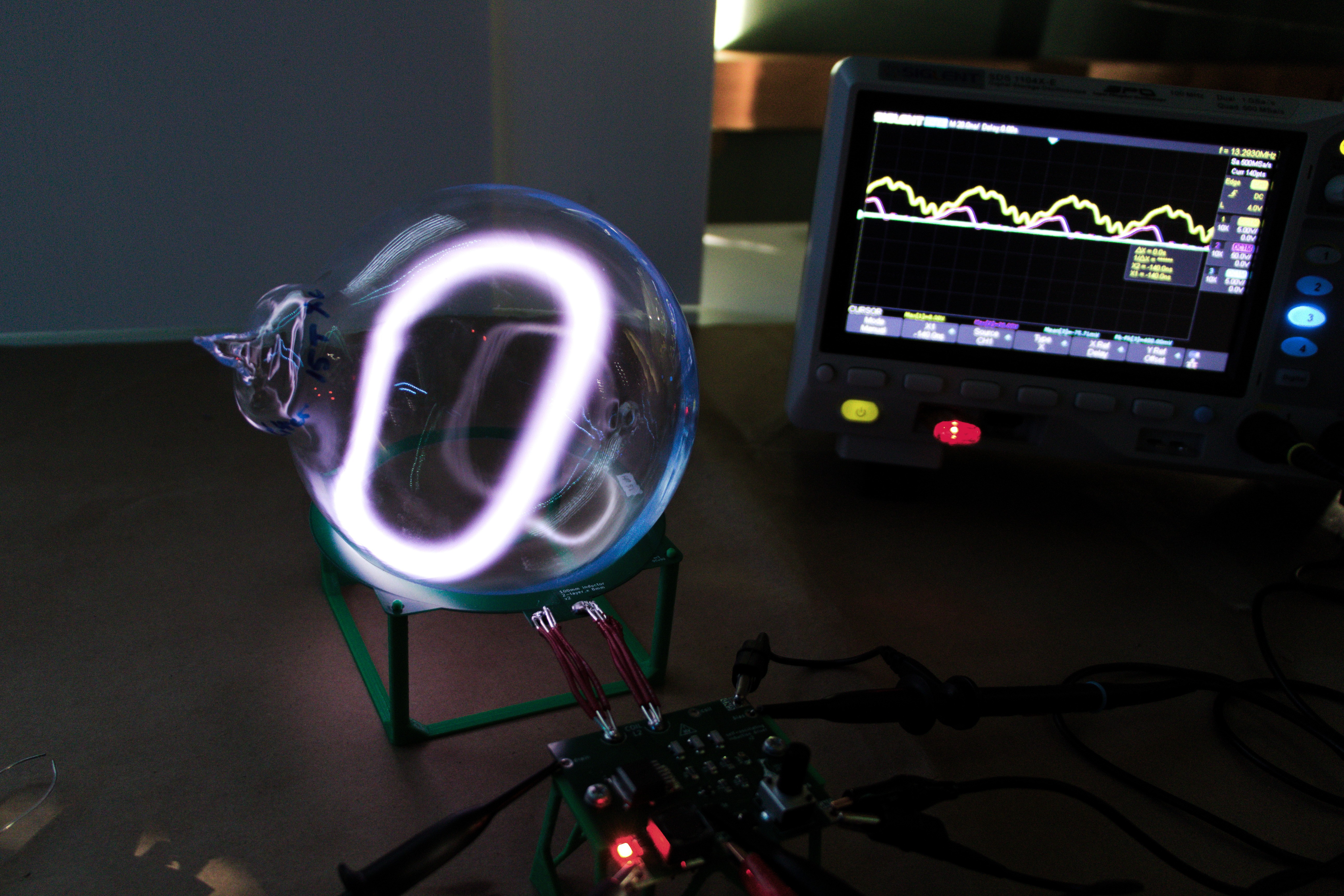
03/11/2024 at 04:20 • 6 commentsRevision 0.3 of the induction driver creates a plasma toroid that's stable and controllable, and does so without overheating.
I'm closing in on a finalized version of the driver. Soon, both the induction coil and driver circuit will be unified into a single monolithic PCB.
This round of prototyping was...Sponsored by PCBWay!
Entirely to my surprise, a representative from PCBWay contacted me with an offer to cover the costs of a batch of boards.
![]()
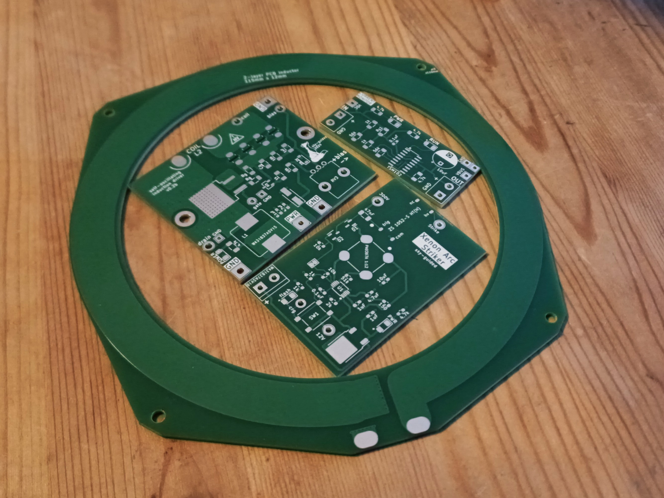
Four boards! Three solder stencils!
(This project log will cover design updates to the induction coil and driver. The other two accessory boards will be featured soon, but there's still a few circuit details I need to refine first.)Some stuff I like about PCBWay:
- Fast. Eerily fast, sometimes.
- Inexpensive!
- Their instant quote functionality can be super handy for design planning, even before a board layout is finished. For example, it's great to be able to test out possibilities for things like "how much would it cost to make the board 50mm wider? What if I want to use 2-oz thick copper?" Etc.
- Quality is solid. Admittedly I haven't plumbed the depths of BGA or wafer-level-packages yet, but for everything I've done so far I've been totally happy with PCBWay boards.
- If there's something malformed in the manufacturing file, a member of their production team will email asking for clarification of design intent. This has happened to me twice!
- I like they that sponsored me. I'm saying that very sincerely, not just because the monetary windfall is nice (although it really is). It's incredibly endearing that PCBWay is seeking out and financially supporting small, independent projects like this one, and not just big-name makers and youtubers that already attract 100k+ eyeballs.
Assembly
Just like previous versions, solder paste was smeared across the laser-cut stencil, components were placed with tweezers, and the board was reflowed on a budget hot-plate.
![]()
(Kapton tape was used to keep the board in place during assembly, but not during reflow.)
Minor soapbox time: I spent quite a while as an electronics hobbyist being intimidated by surface-mount parts. Secret is, SMD assembly (at least for relatively large components) is faster and easier than strip-board and through-hole. This is especially true with a solder stencil and hotplate (or presumably toaster oven) reflow. Through-hole parts are decidedly obsolescent, and these days most interesting ICs are only available in surface-mount. For this project, using an actual PCB is also hugely important for minimizing parasitic inductances.
![]()
With a larger inductor coil (115mm center-span x 12mm width) and some neater connecting wire bundles, the assembly looks pretty slick!
Here's what changed in driver version 0.3:---------- more ----------No more overkill SiC MOSFET
I'd been considering replacing the Qorvo UJ4C0750 - series SiC mosfet for a bit now. Some of that motivation was due to their cost (at ~$11 each), but performance characteristics drove the change.
I'm now using the Infineon IPB17N25S3-100 "OptiMOS" Si mosfet instead.
For this application there were a few key parameters, at least as I understand them:Drain-Source voltage: Never seemed to rise above 200V in either simulation or on the bench. Absolutely no need for the 750V-rating of the UJ4C0750. The IPB17N offers 250V, which is plenty.
Drain Current: Needs to be anywhere upwards of 6 amps or so. Again, the new mosfet has plenty of headroom at 17A.
Gate Charge: Without a proper high-current mosfet driver, it seems worthwhile to minimize the amount of charge that needs to be shoved in and out of the gate pin before the device switches. The UJ4C's 37nC is ok, but the IPB17N has a gate charge of only 14nC.
Switching speeds: Longer switching times could result in greater switching losses. Delay and rise/fall times on the IPB17N are as little as a couple of nanoseconds, compared to low tens of nanoseconds for the UJ4.
Output Capacitance (Coss): Steve Ward stresses the importance of C(oss) being fully discharged before switching, and discusses the (possibly substantial) heating due to capacitively stored energy. The UJ4C has a quite low C(oss) value. I almost certainly overemphasized C(oss) as a parameter, which is a big part of what lead to using the UJ4 in the first place.
On-resistance: The UJ4C has an quite low On-resistance of only 58mOhm. It's a bit higher for the IPB17N at 85mOhm, but not that much higher. At the low operating currents of 2-3 amps, it hardly makes a difference.
Basically, parts in the OptiMOS series look super good enough, at about a fifth the price. A lot of the offerings in Infineon's CoolMOS product line also look quite compelling by the numbers, but Steve Ward warns about that SuperFET type device often having unexpected energy losses. I'm increasingly unsure how much I trust that (especially given the CoolMOS datasheets explicitly list C(oss) energy figures that are rather low), but for the moment I'm using the OptiMOS -- and a lot of that decision was fueled by seeing someone else's highly successful build using parts from the OptiMOS series, as I'll discuss in a moment.
Unfortunately, the device footprint of the IPB17N wasn't compatible with the UJ4C, otherwise I'd probably have just bodged other design changes on to the version 0.2 board.
Lesson learned: do not be seduced by new hotness semiconductors unless I have a specific reason to need their characteristics.The magnificent plasma toroid of Humxn
Recently, a youtube user by the name of Humxn posted a video of their own plasma toroid. Not only is their build cool and clean, they also do a fantastic job of walking through both design details of their (very tidy) circuit, as well as a number of implementation tips and tricks. Humxn also showcases a beautifully stable toroid that can float perfectly in the middle of the xenon globe.
I'm borrowing several design elements directly from them:
- Use of the OptiMOS series mosfet, rather than the CoolMOS I'd been eyeing.- Using a zener diode to create a voltage reference for the gate bias, rather than just a raw voltage divider from the supply line (which destabilizes if voltage sags due to hitting supply limits). As soon as I saw the zener, I mentally facepalmed at not having considered it sooner.
- Understanding that reduction in driver power helps the toroid float and stabilize. I had assumed that floating was due to high drive power and lots of convection from plasma heating. I'd had it exactly backwards!
- Adding a mm or two of separation between the drive coil and the glass globe (my new inductor revision has a bit of blank space between the inner diameter and the copper trace).
- A greater appreciation for current-control as a way of manipulating toroid behavior.
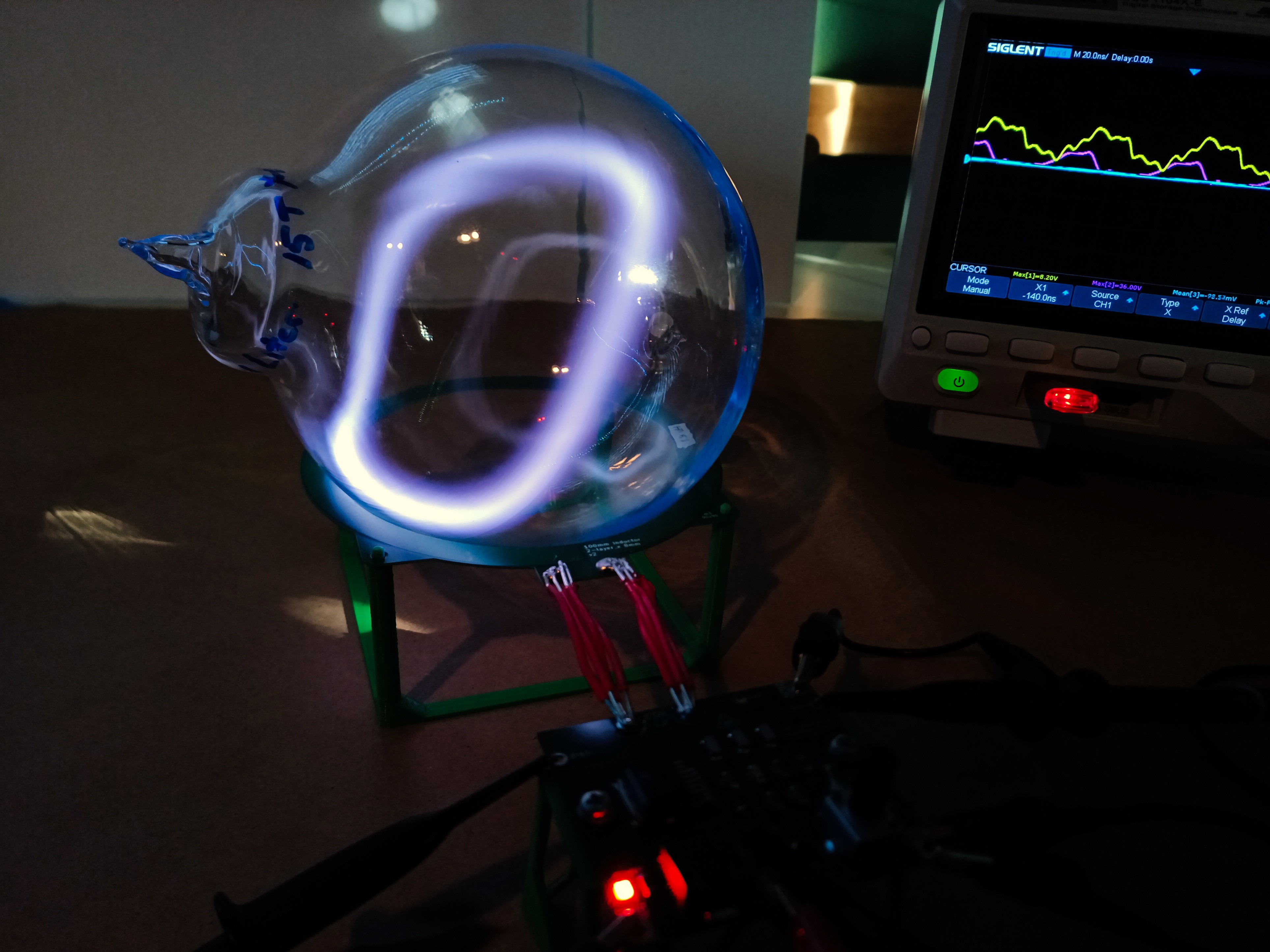
If you're at all interested in building your own plasma toroid machine, the Humxn video is absolutely essential.Testing Results
Video is at the top of this log :)
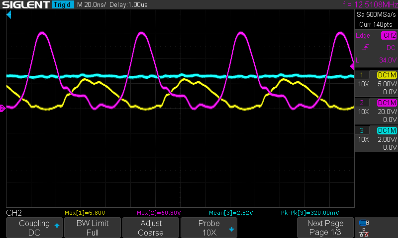
Here's the scope traces with the xenon going full donut.
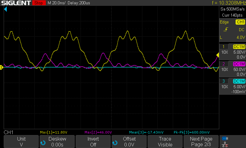
![]() As previously, the yellow trace is gate, purple is drain, and blue is gate bias (note the different y-axis scale). Those waveforms look basically ideal (and I think some of the remaining wigglyness on the drain is due to mediocre scope probing, since I only have so many hands to use pokey leads and not clips). The shape on the drain trace does morph a bit in response to changing drain voltages.
As previously, the yellow trace is gate, purple is drain, and blue is gate bias (note the different y-axis scale). Those waveforms look basically ideal (and I think some of the remaining wigglyness on the drain is due to mediocre scope probing, since I only have so many hands to use pokey leads and not clips). The shape on the drain trace does morph a bit in response to changing drain voltages.
The L1 input choke inductor value was increased to 6.8uH. The previous 2.2uH inductor had been chosen low in an attempt to constrain circuit power draw, but tbh I really should have just planned on setting limits on the supply side.
Adding a 1nF rf-bypass capacitor to the bias voltage network does indeed smooth out that waveform. (Also, turns out I had once again been seeing spurious wigglyness due to an over-large loop area with the ground clip.) Replacing the bias voltage divider with a zener reference also makes striking the toroid quite a bit more stable and reliable. I'm currently using an 8.2V zener but will swap it down to 4.7V soon, to make better use of the full potentiometer range.
I'm realizing that everything I said previously about the using a bias smoothing cap and increasing the impedance between bias and gate-drive causing "runaway oscillation" was total nonsense. Upon further testing, it now seems like the Miniware PSU just dealt poorly with rapid changes in current demand if the circuit ramped to full oscillating power too quickly. This was easily fixed by adding more bulk capacitance at the circuit's supply hookup.Thermals
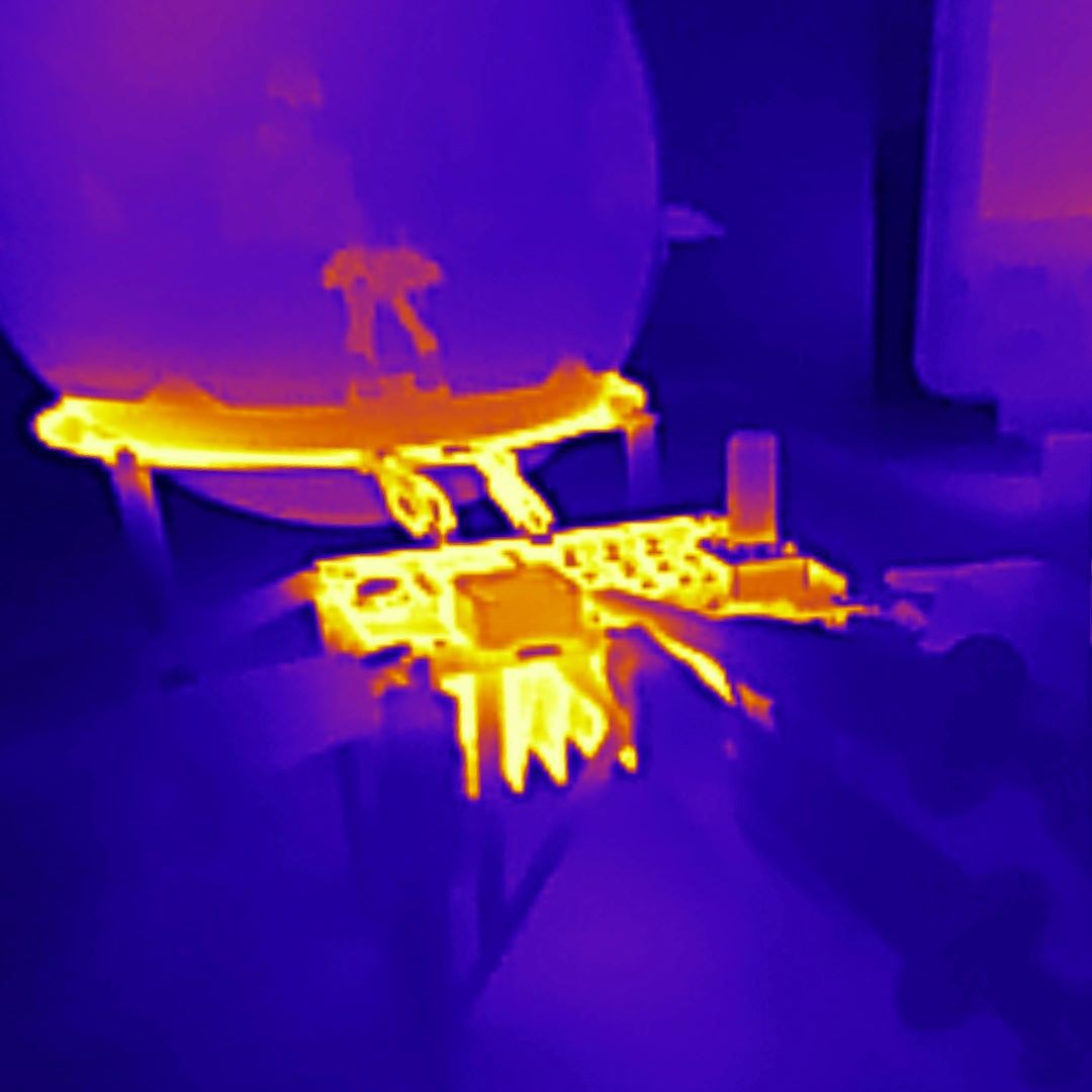
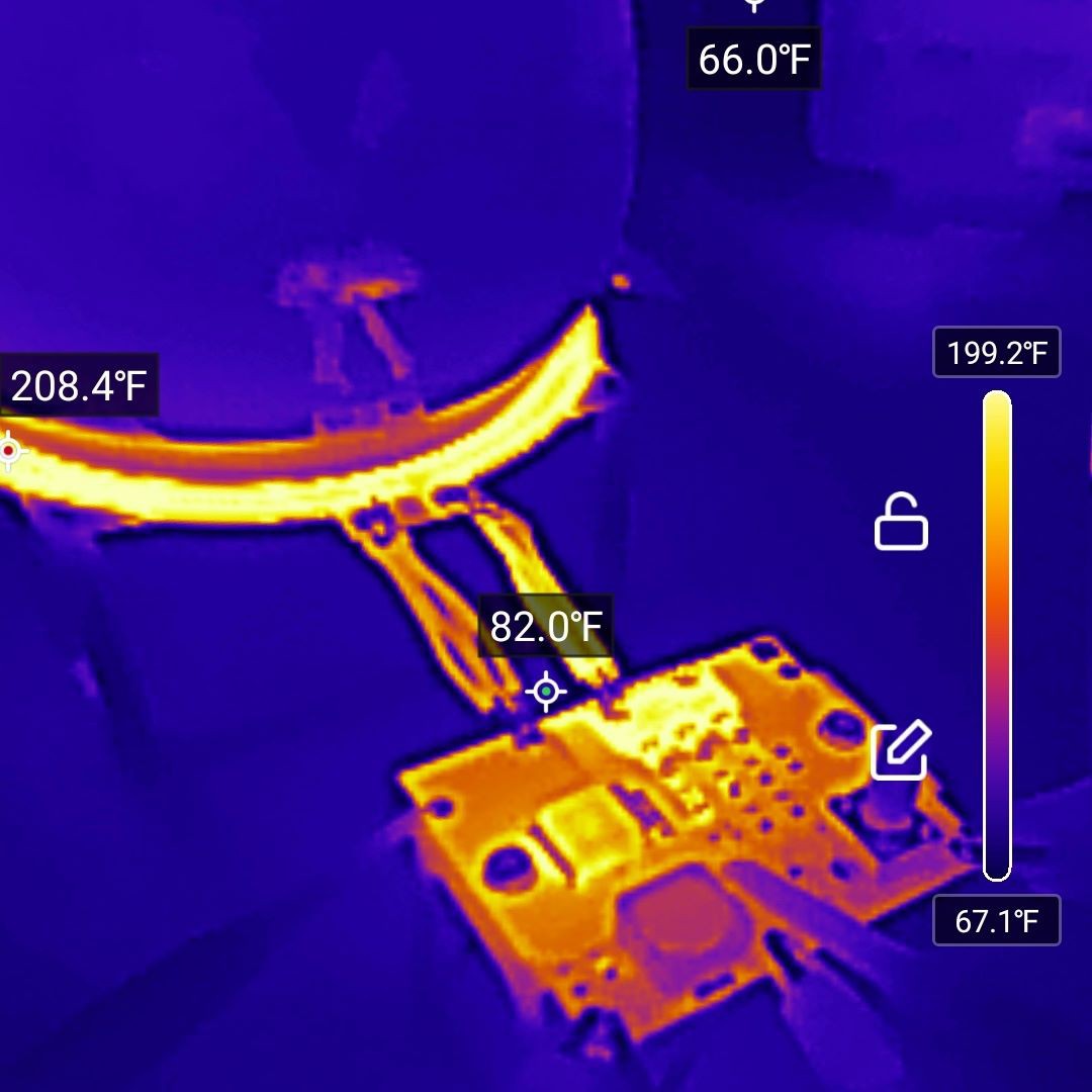
Manageable! Running the stabilized toroid at 25-30 watts, the hottest part of the whole project is the globe glass.
![]()
Increasing the trace width of the PCB inductor has helped a lot -- temperatures stayed <50C, or even cooler when the toroid was running at low power.
Performance of the new mosfet is similar to the previous driver iterations. At low power, temperatures (measured infrared at device body) are <60C. Running at full 60-watt power the mosfet still gets probably too hot; 120-130C. I may end up using two mosfets in parallel in the final version. It's definitely not ideal to run at full power for very long (and it seems to offer very little visual benefit anyway), but tightening the envelop of maximum supplied amperage does seem to make the arc start a bit less reliable, when hitting the regulation limit causes the supply voltage to be lowered.
The under-board heatsink has also been mounted and re-mounted several times now, and it's possible that its thermal interface layer isn't making very good contact.
There's a teeny hot-spot on the gate drive resistor. I'll plan on two parallel 1206-size resistors for the next version.
When the toroid isn't ionized, there's quite a bit of heat buildup on the high-voltage side of the (now) four-capacitor primary bank. It's hard to tell for sure, but I think the copper itself is getting hot rather than the capacitors (especially since the gate side of the cap bank stays cool). I'm wondering if parallel-plate capacitive coupling to the ground plane might be causing dielectric losses in the fiberglass? I genuinely don't know if that conjecture makes any kind of sense -- please let me know if that's totally implausible.
Here's my favorite photo from this project so far:
![]()
When the toroid is stabilized it looks, honestly, unreal. A little ring of light that floats perfectly centered, still and silent. The dynamic range of the camera can't quite keep up with the plasma's brightness -- IRL it looks more nebulous, more ghostly. (It also plays havoc on camera auto-focus.)
NEXT STEPS:
A key design goal is running the toroid standalone off of USB-C. To that end, I'm implementing built-in power monitoring to indicate whether or not the circuit is in oscillation, rather than needing to read PSU loads or oscilloscope waveforms.
I also very much want to have push-button start for the plasma ionization, rather than the (kinda crude) method of twist-rubbing the globe against the coil.
Unfortunately, neither of those features is working quite yet.
Stay tuned. -
#4: tweakin'
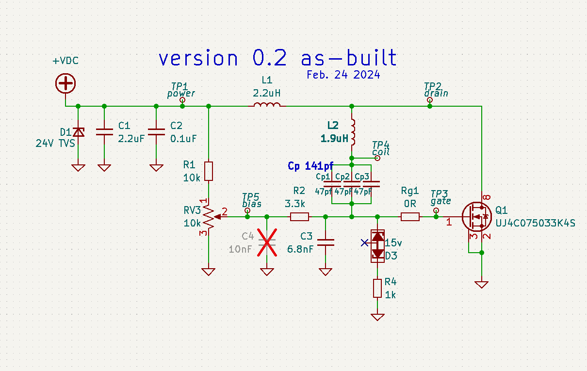
02/25/2024 at 21:36 • 0 commentsSpent a big chunk of the weekend adjusting a variety of component values.
![]()
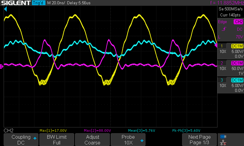
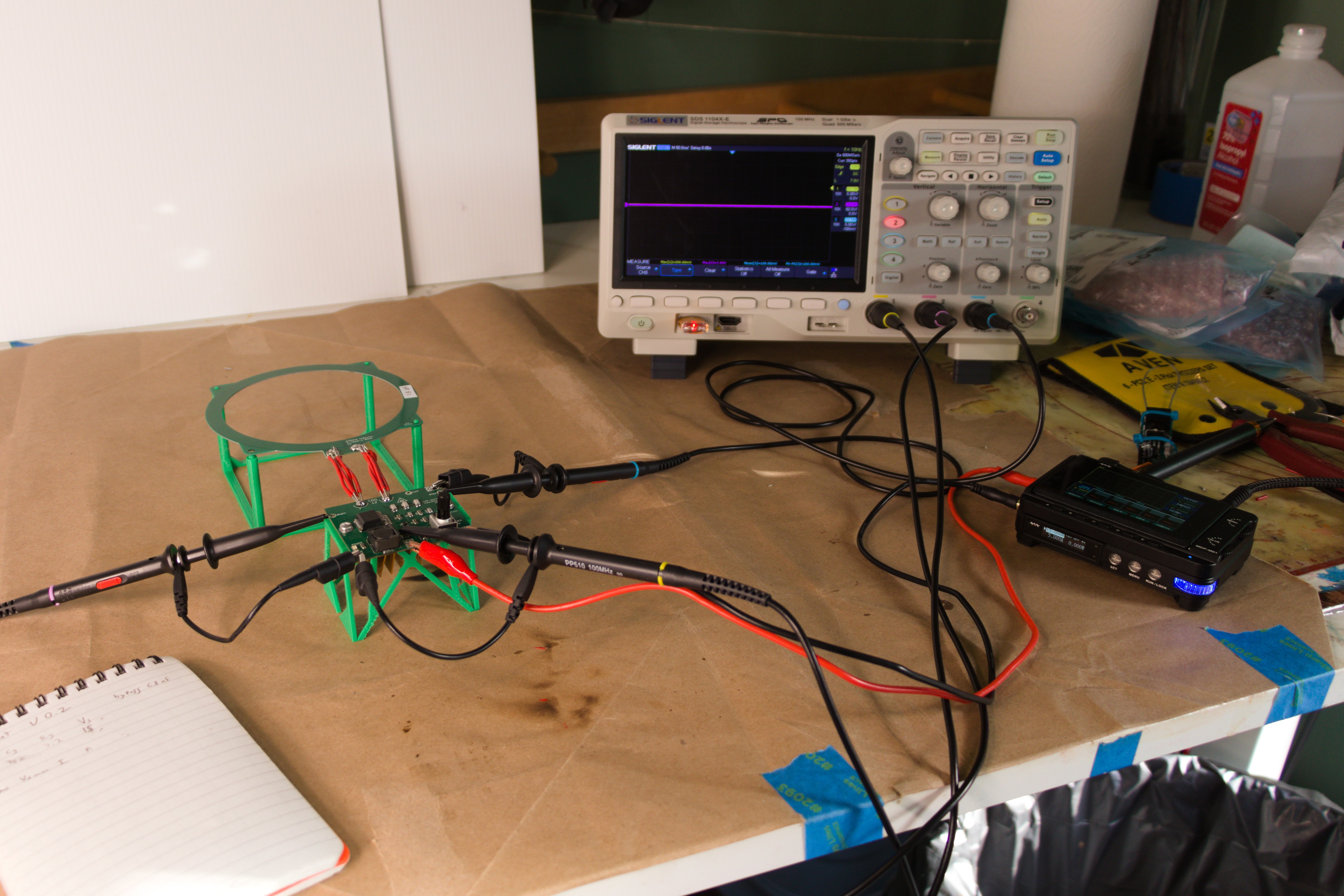
Here's the waveforms with the circuit unloaded (no toroid), at 18V supply:![]()
Yellow is Gate (5V/div), purple is Drain (50V/div), blue is feedback network bias input at TP5 (5V/div).
Looks decently healthy to me. I suspect that the gate protection zener diode is doing its job and helping to keep drive voltages within operational limits.
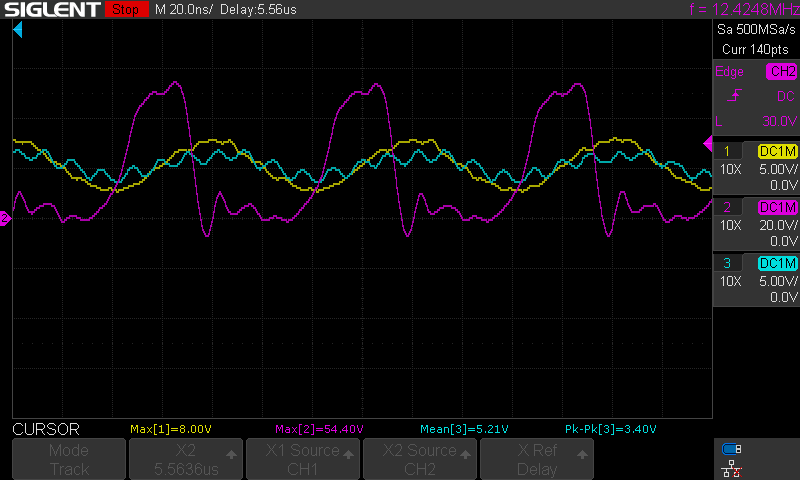
Here's the traces when the xenon is fully toroid-ing:![]()
Hm. Clearly the device is overall functional but these waveforms aren't as clean as I'd prefer. Maybe it's fine? [EDIT: as before, turned out a lot of the wiggliness was from bad probing. Shorten those ground connections!]
All right, so let's walk through the component changes. I'll spare the step-by-step of each individual test -- most of it was poorly documented and I was going for more of a "better or worse?" approach than robust characterization.
First off, primary tank capacitance was increased 99pF to 141pF. This was the first change made, as planned in previous project log "i would like my circuit to not cook myself".
Increasing capacitor value was broadly successful -- overall power draw was reduced to ~2.9 - 3.2A depending on circuit configuration. Yay!
Decoupling cap C4 was removed because it caused some kind of runaway oscillation on both gate voltage and power draw. A different cap value might be fine but for the moment, the pads are empty. [EDIT: the problem was that a cap here caused input power to ramp up faster than supply power could keep up with. The solution was more bulk input capacitance!]
I spent quite a while trying to increase operating gate drive voltages. You can see in the second pic that gate drive peak is only 8V, when I'd have preferred something closer to 15. My understanding is that MOSFETS really prefer to be driven by a square wave rather than this sinusoidal feedback. With intermediate voltages near the switching threshold the mosfet is in a state of "kinda-on", which causes a lot more power loss (and thus heat) than being fully on or fully off.
I was hoping that larger values of R2 would strengthen gate drive and increase the differential between the gate voltage and the (still too wiggly for my taste) bias voltage. Initially I spec'd R2 for 10k in this iteration, but it turned out that overly large values resulted in too tenuous of a ground reference. The max stable value I tested was 3.3k for R2.Similarly, decreasing gate capacitor C3 to 6.8nF increases gate drive voltage a bit, but it's not as dramatic a difference as I'd have expected.
Playing with the gate resistor Rg was a bit odd. Looking at the traces I saw very little change with values ranging from zero ohm to 10Ω. Subjectively, 0Ω seemed to cause the least heating of the mosfet, but I wasn't taking rigorous enough measurements to say that with certainty. (Also, the 10Ω resistor almost immediately toasted itself; the gate capacitance is slurping far more power than a little 1206 smd can handle.) I wasn't able to observe any kind of difference in probable turn-on delay based on scope measurements.
Looking back at the drain traces in the toroid-loaded condition, I see a couple of things:
- Drain voltage peaks at only 55-65V or so.
- Drain ringing after turn-on, including temporarily shooting negative.
I don't even know if either of those is even really a problem. I may investigate using a higher inductance feed coil L1 -- other folks describe 10uH, I'm only using 2.2k. Might also look into a schottky diode across the mosfet to clamp drain against going negative.
Returning to the topic of board thermals:
The key discovery was that heating on the inductor coil and the primary capacitor bank goes way
down when the xenon is actually ionized toroidal. I believe this lends some credence to the idea of framing coil heating in terms of "input energy has to go somewhere".
I also hooked up a little 40mm axial fan and aimed it at the board heatsink, and stuck a teeny copper heatsink on top of the mosfet.![]() With all of the changes, I was able to get temperatures to stabilize at ~100-110C on the mosfet body and ~50-60C on the coil while the toroid was active.
With all of the changes, I was able to get temperatures to stabilize at ~100-110C on the mosfet body and ~50-60C on the coil while the toroid was active.![]() That's hotter than I'd like, but... basically fine. It means that at the moment I can run the device for minutes at a time without worrying about it bursting into flames. Still probably worthwhile to use coil with wider traces, use more capacitors in the primary bank to spread out the load a bit, try to reduce mosfet losses, etc. Again though, yay!
That's hotter than I'd like, but... basically fine. It means that at the moment I can run the device for minutes at a time without worrying about it bursting into flames. Still probably worthwhile to use coil with wider traces, use more capacitors in the primary bank to spread out the load a bit, try to reduce mosfet losses, etc. Again though, yay!Stay tuned for more!
-
#3: i would like my circuit to not cook itself
02/16/2024 at 03:22 • 0 commentsFirst Light accomplished. What did I learn?
The circuit in its current iteration,
1: gets hot alarmingly quickly
2: is trying to draw more power than I can actually supply.
Those seem related, yeah.![]()
apologies for the excessively american temperature units
Based on simulating the circuit in the condition tested, at 15 volts supply I'd expect to see something like 50W power draw, at around 3.5A. The tests discussed in the previous post sure looked like the USB-based bench supply was badly voltage sagging, so the next day I hooked up the beefier bench supply -- and very quickly started sagging, then blew another mosfet. I suspect that this very-budget bench supply has some sort of destructively un-graceful switch from constant-voltage to the constant-current mode it failovers to when it hits 5A, but it's also entirely possible that the mosfet blew first and I saw the power supply feeding a shorted chip.
My power budget is <5A @20V (the 100-watt maximum of USB-C-PD), but I'd prefer to stay <60W if possible.---------- more ----------
If I simulate a lower primary capacitance (e.g. 66pF instead of the as-built 99pF), power draw is dramatically greater and the higher resonating frequency is also a closer match to what I observed on the bench. Same thing if I sim a lower inductance value. (This relationship of LC values and frequency is of course exactly what you'd expect just from looking at the series LC equation, but the effects on power I hadn't thought ahead to anticipate.) Based on the cap data sheets I wouldn't expect a huge de-rating but who knows. It's also possible there was error in measuring inductance values -- I don't have an LCR meter, so I set up a little parallel LC circuit that I drove with a square wave and o-scoped the resultant ringing.
Takeaway: I can likely offset observed power-hungriness with either a higher-value capacitor bank or primary inductor.
Adding more capacitance is pretty easy, so that's my next step. I may also investigate making a four-turn PCB inductor, but I'd prefer the wide open traces of the two-turn (plus two-turn make it easier to route traces for the ionization pilot arc, which is a topic for future discussion).
On the topic of the PCB inductor getting super hot: based on sims I expected ~10 peak amps in the primary inductor, or maybe 12A at the very worst. PCB trace width calculators using IPC-2221 or -2152 thermal design guidelines predicted temperature rises of <30°C. I observed temperatures shooting past 130°C within about thirty seconds. Either I'm getting quite a bit more current than expected, or the thermal design formulae don't apply here.
If I plug numbers into the SaturnPCB Toolkit -- a load current of ten amps, an 8mm x 600mm 1-oz trace, and a frequency of 13MHz -- it tells me to expect a power dissipation of about 3.2 watts. One thing the formula doesn't consider is that the inductor coil has two conductors stacked on top of each other. I also notice the toolkit is only estimated 0.02Ω DC resistance, so of course if I scientific wild-ass guess an actual resistance of 0.2Ω I'd expect ten times as much heating. That's a better match for my sensibilities for how immediately cookin' things got.
On a more fundamental level though, if the device is overall drawing 50-60W, that energy clearly has to go somewhere. Physically I'm not sure where I should expect the balance of energy to go. There's gotta to be some combination of circuit waste heat, energy delivered to the plasma, and energy emitted as legally-dubious radio waves. I'd hoped that the latter two would be the majority, but that was based more on optimism than analysis.
In any case, I'm going to try to bring the overall power draw down first, then reevaluate where I'm at on the coil temperature. The few other examples I've seen of this project all use copper tube coils so it's always possible that a PCB coil just isn't viable, but I'm far from ready to give up.
The coil isn't the only thing heating up though! Reducing overall power might help, but there's more I can learn from the first v0.2 tests.
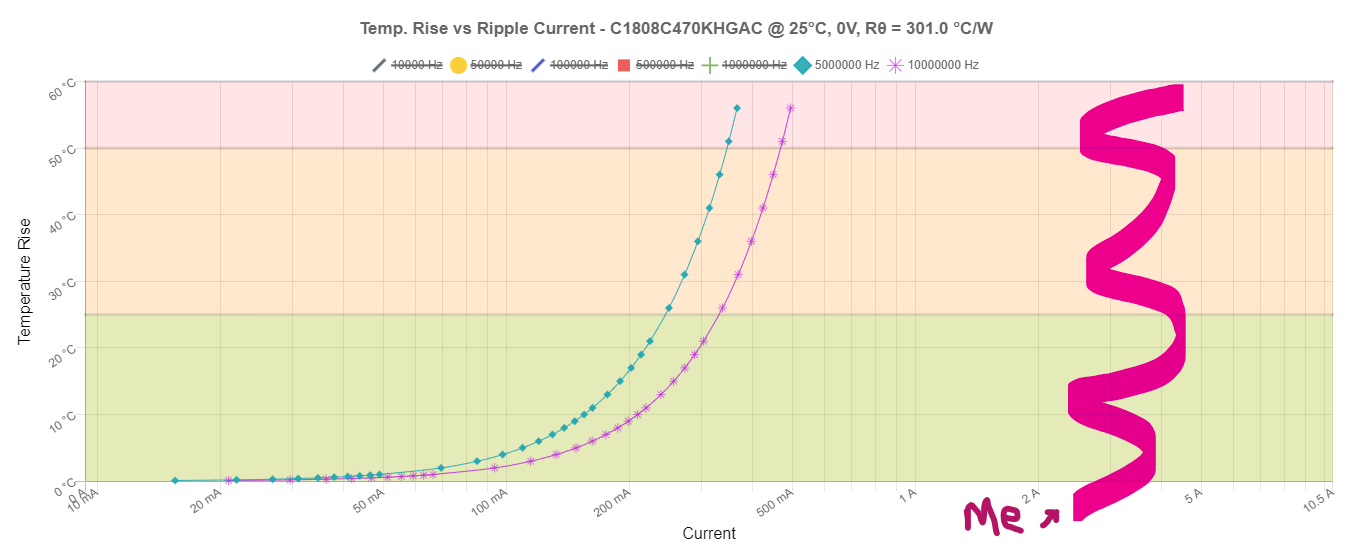
Managing heating in the capacitors can be addressed by adding more capacitors. If I use six caps instead of three, by the simple magic of P = I²R I should expect a quarter of the heating.
I couldn't find thermal specs for the TDK capacitors I've been using, but looking at Kemet design tool for the next-iteration caps, and, well![]()
Yeah that aint' great. 301C°/W feels a bit pessimistic but I don't have enough intuition yet to really know.
For the next board revision I can also consider dropping some thermal vias towards the heatsink underneath, and/or using SMD thermal jumpers to suck heat towards the ground plane.
On the topic of the heatsink -- based on the thermal cam it definitely looked like the heatsink was getting toasty, which is a good sign for it being decently well coupled to the mosfet. However, after thinking about it for more than five seconds I realized that I really ought to be keeping the heatsink cool because an already hot heatsink can't sink heat.
I knew that a fully-passively-cooled driver circuit was likely overambitious but I wanted to give it a go. Looks like I may have to install a fan (and possibly a bigger heatsink) anyway.Further experimentation will mean soldering on a new mosfet. That''ll require not only removing the heatsink, but also scraping off the phase-change thermal interface shmoo that's oozed all over the place only to squeeze into one thin layer for next tests. I've been putting that off for a few days, but it's gotta get done sometime.
Stay tuned, dear reader. -
#2: v0.2 -- First Light!
02/10/2024 at 02:41 • 0 commentsI'll put the cool part right up top: it works.
![]() (and i blew up zero mosfets in the process!)
(and i blew up zero mosfets in the process!)
Version 0.2 boards arrived lookin' nice and spiffy.![]()
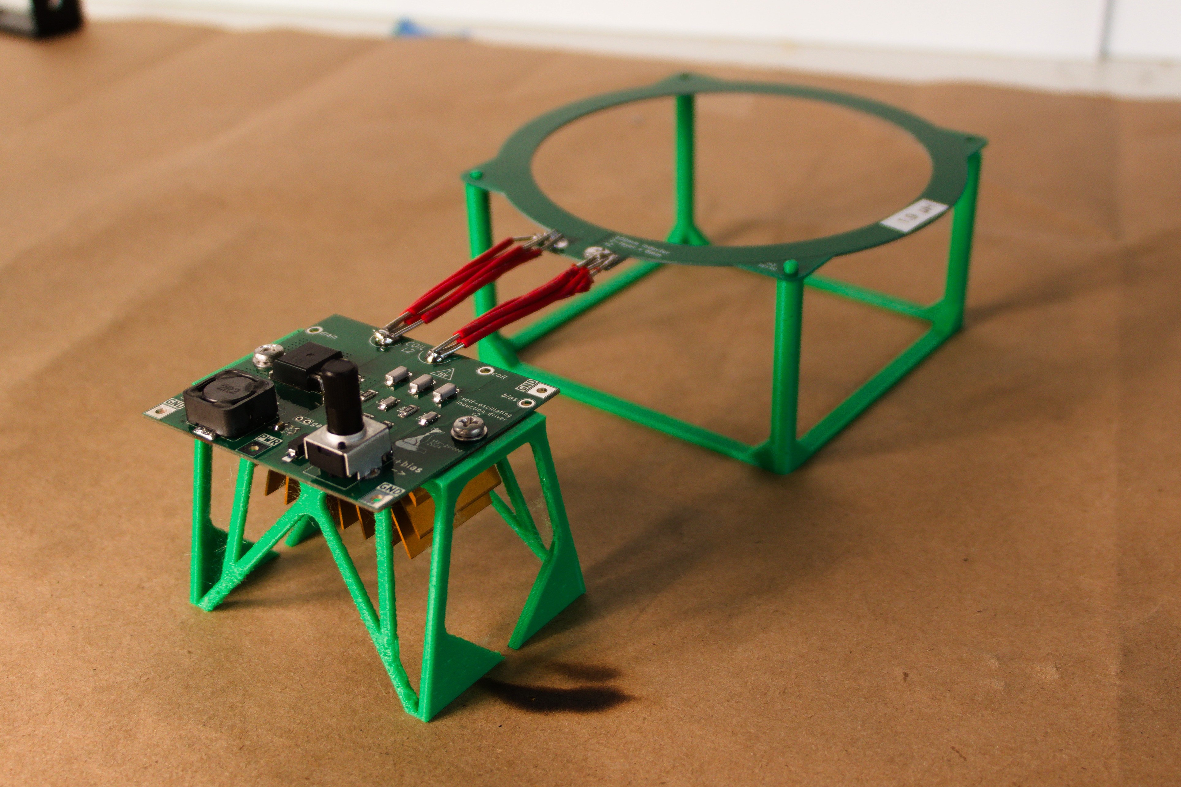
Everyone else I've seen who does a variant on this project uses a primary inductor made either of regular wire or copper tubing. I thought a PCB inductor would be more elegant. This inductor is two stacked turns on 0.6mm PCB, 100mm center span and 8mm wide. I measured the inductance to be about 1.9µH.
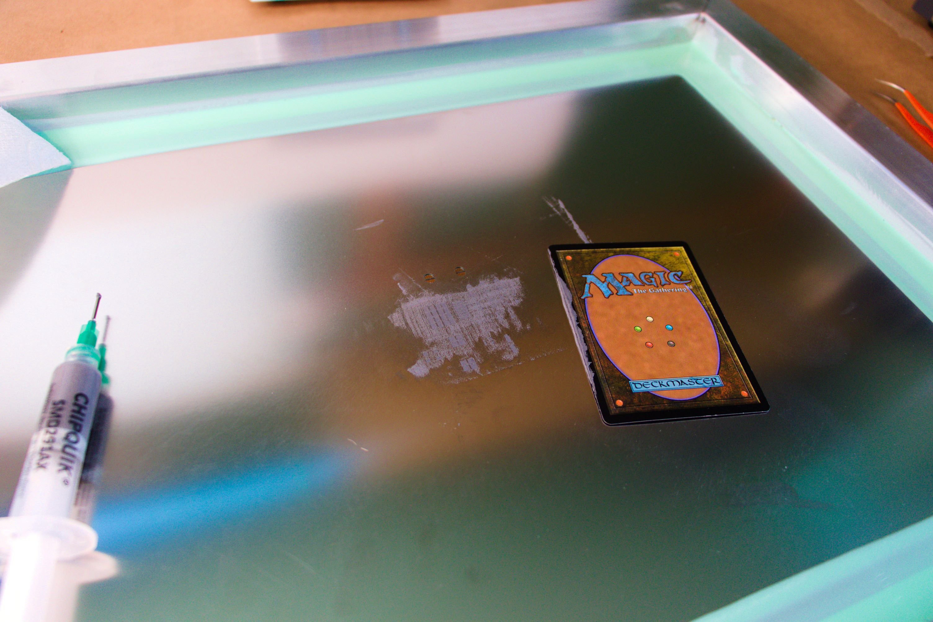
This was my first time using an actual solder stencil and hot-plate reflow rather than daubing on solder paste and using the hot air station. Turns out, using an actual stencil is way easier. Who'd have thought. Also turns out a scrap MTG card is a great paste spreader -- thanks to my gf for the improvised tool 🌈✨![]()
Soldered up beautifully.
![]()
Since previous test coils had their 18ga wires badly overheat, I used bundles of 4x18ga to connect the board and test inductor. This is either a hacky kludge to get more surface cooling area, or a way of making bootleg litz wire -- take your pick.
---------- more ----------
Heatsinking for the mosfet is on the bottom side of the board -- you can see some of the orange fins peeking out. (There was an odd misadventure of the board flexing and making poor contact with the heatsink until I was able to melt down the kinda-thick phase-change thermal interface pad with the hot air station.)
I designed the board to use a duo of 0.1µF and 10µF capacitors for input power smoothing/decoupling... then realized during assembly that in my capacitor kit, those values aren't rated to enough voltage. 6.8nF was the highest value that fit in the 0603 footprint with a 50V rating. Fortunately the power input looked stable enough under load.![]()
I spent quite a while futzing with the circuit and adjusting components trying to track down what looked like self-oscillation. Turns out nah I was just being a silly goose; the potentiometer was upside-down relative to v0.1 and I'd been turning it the wrong way, in spite of having triple-checked during board layout and marking the orientation on the board.
![]()
Clearly still needs some tuning but this is the basic waveform I expected. Yellow trace is gate (5V/div), purple is Drain (50V/div). Interestingly I was able to get strong oscillations and a running toroid even at 12V supply, when BackMacSci talked about 18V being the minimum for his setup. I'm hoping that adjusting Rg will reduce some of that higher-frequency ringing. [EDIT: Turns out this was mostly poor probe technique!]
The PCB inductor still gets immediately and disconcertingly hot, even with much more dissipation area that the initial wire coil.![]() There's also distinctive heat buildup around the primary capacitors. Downsizing to a bank of three (from five) might have been asking a bit much.
There's also distinctive heat buildup around the primary capacitors. Downsizing to a bank of three (from five) might have been asking a bit much.
Good news is that the underside heatsink is indeed sinking heat. The mosfet gets hot quickly too, but I'm hoping better circuit tuning will help.![]()
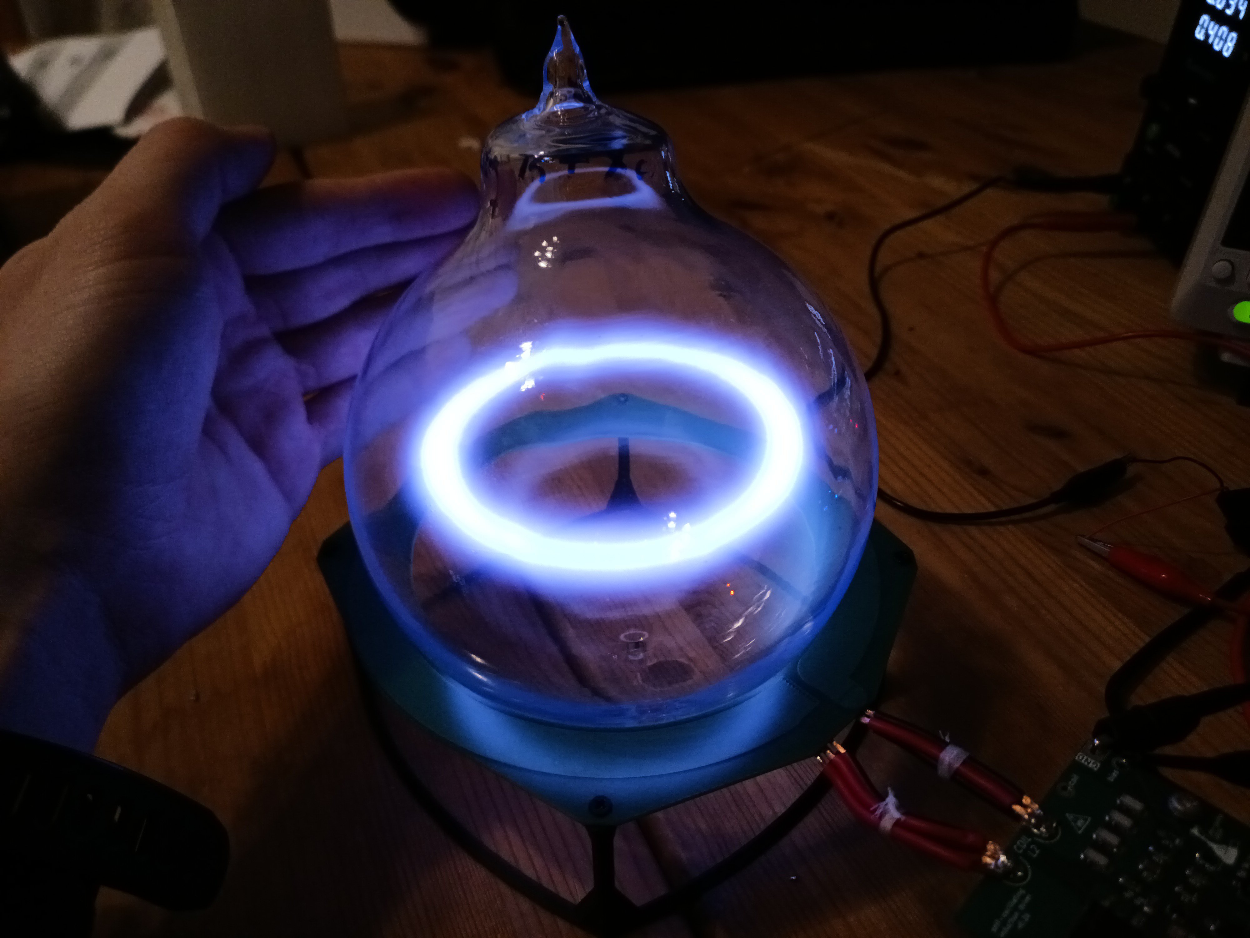
Here's another photo of the toroid:
![]()
You can see that the o-scope waveform is all wonky when the toroid is actually toroid-ing.
For these tests, I was using a Miniware MDP-XP power supply. I'm a big fan of that tool -- it's tiny, usability is great. It also runs off of USB-PD, and in tracking down a variety of odd behaviors I ascertained that the USB power brick I was using may have been rated to 20V and 5A... but not both of those at the same time. Full load was causing substantial voltage sag.
Next tests: a beefier bench PSU. Stay tuned!
Plasma Toroid (sky-guided PCB edition)
inductively-coupled radiofrequency plasma toroid in xenon gas
 As previously, the yellow trace is gate, purple is drain, and blue is gate bias (note the different y-axis scale). Those waveforms look basically ideal (and I think some of the remaining wigglyness on the drain is due to mediocre scope probing, since I only have so many hands to use pokey leads and not clips). The shape on the drain trace does morph a bit in response to changing drain voltages.
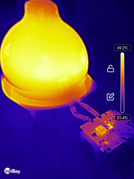
 With all of the changes, I was able to get temperatures to stabilize at ~100-110C on the mosfet body and ~50-60C on the coil while the toroid was active.
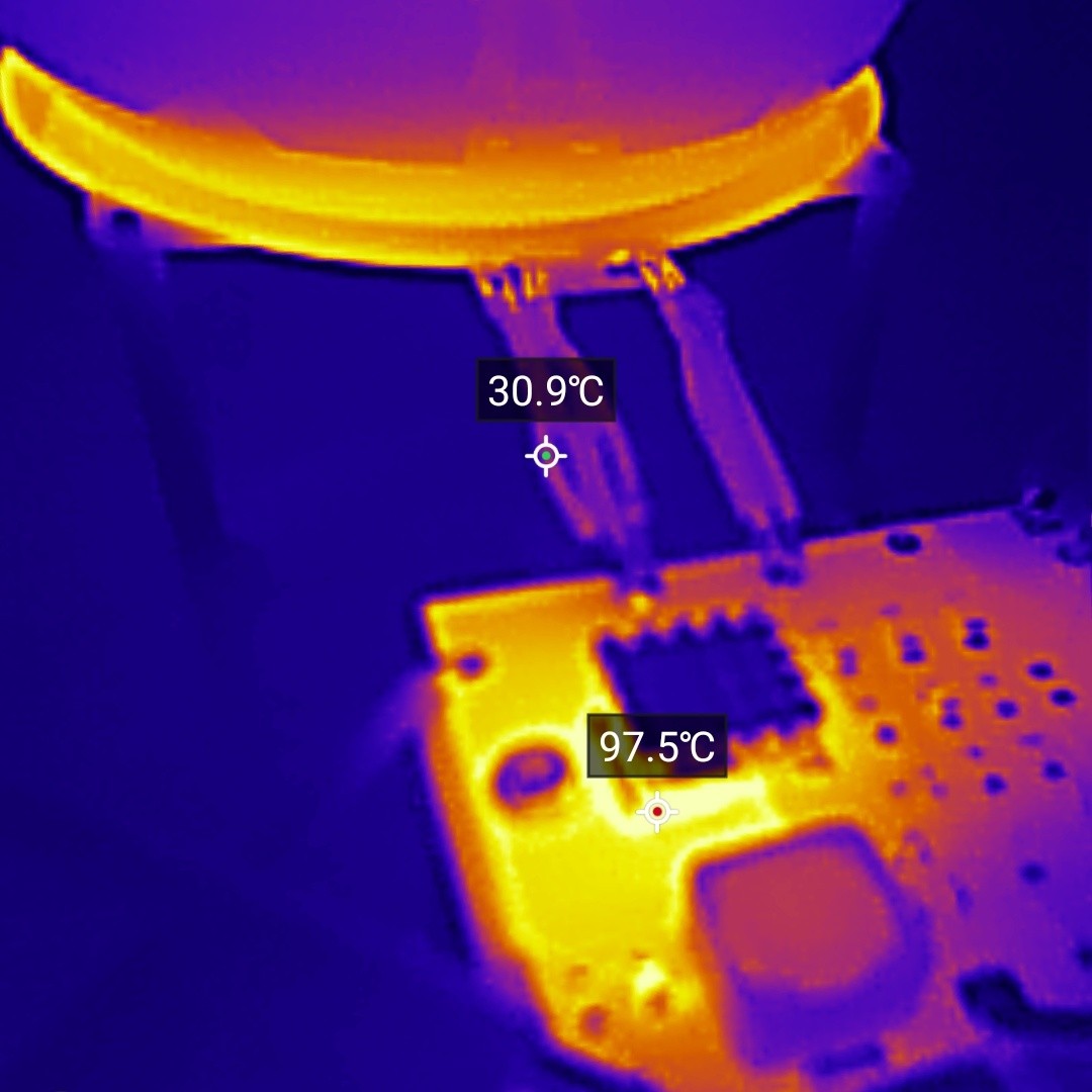 That's hotter than I'd like, but... basically fine. It means that at the moment I can run the device for minutes at a time without worrying about it bursting into flames. Still probably worthwhile to use coil with wider traces, use more capacitors in the primary bank to spread out the load a bit, try to reduce mosfet losses, etc. Again though, yay!
 (and i blew up zero mosfets in the process!)
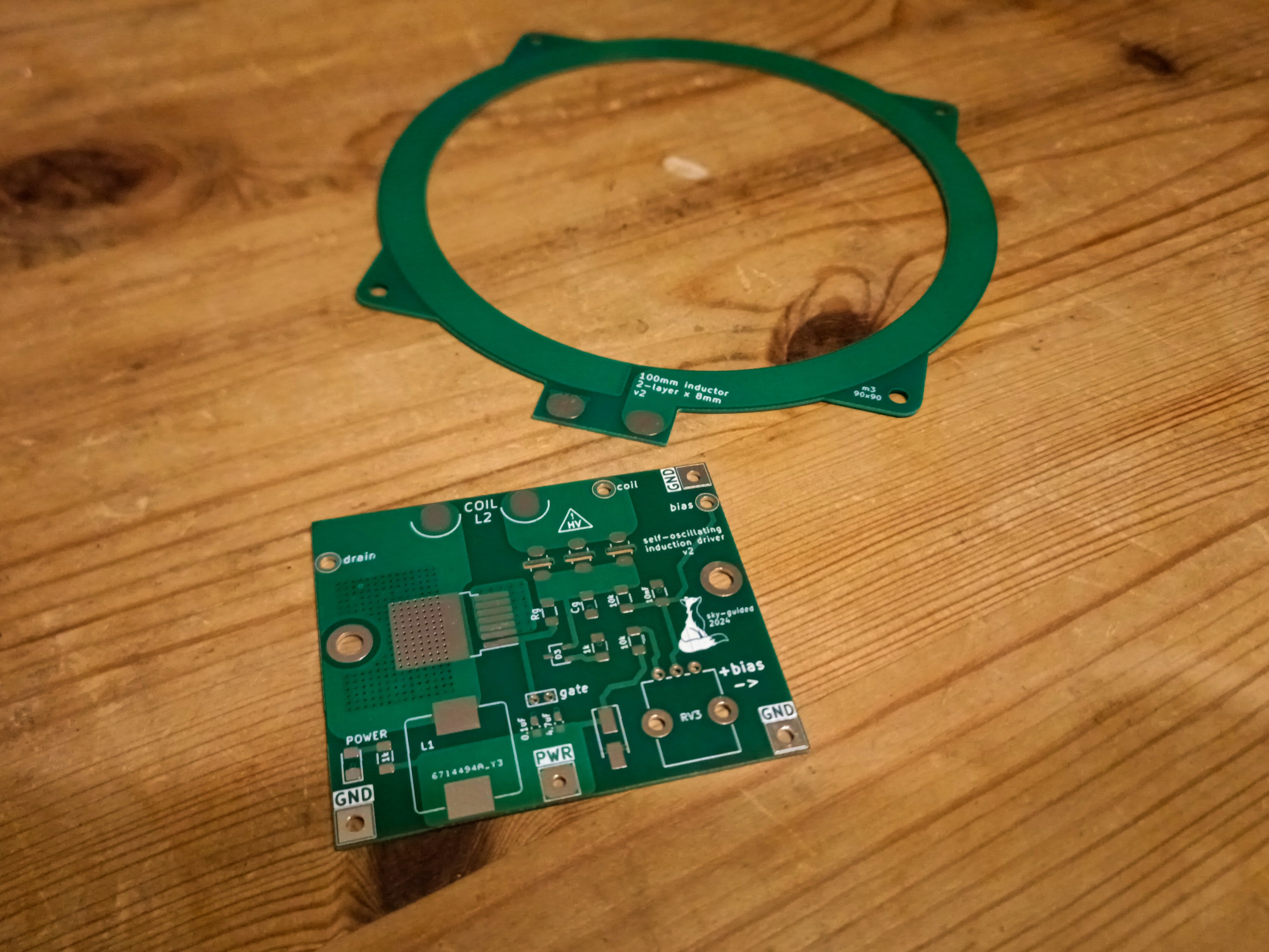
 There's also distinctive heat buildup around the primary capacitors. Downsizing to a bank of three (from five) might have been asking a bit much.