sky-guided
-
#4: tweakin'
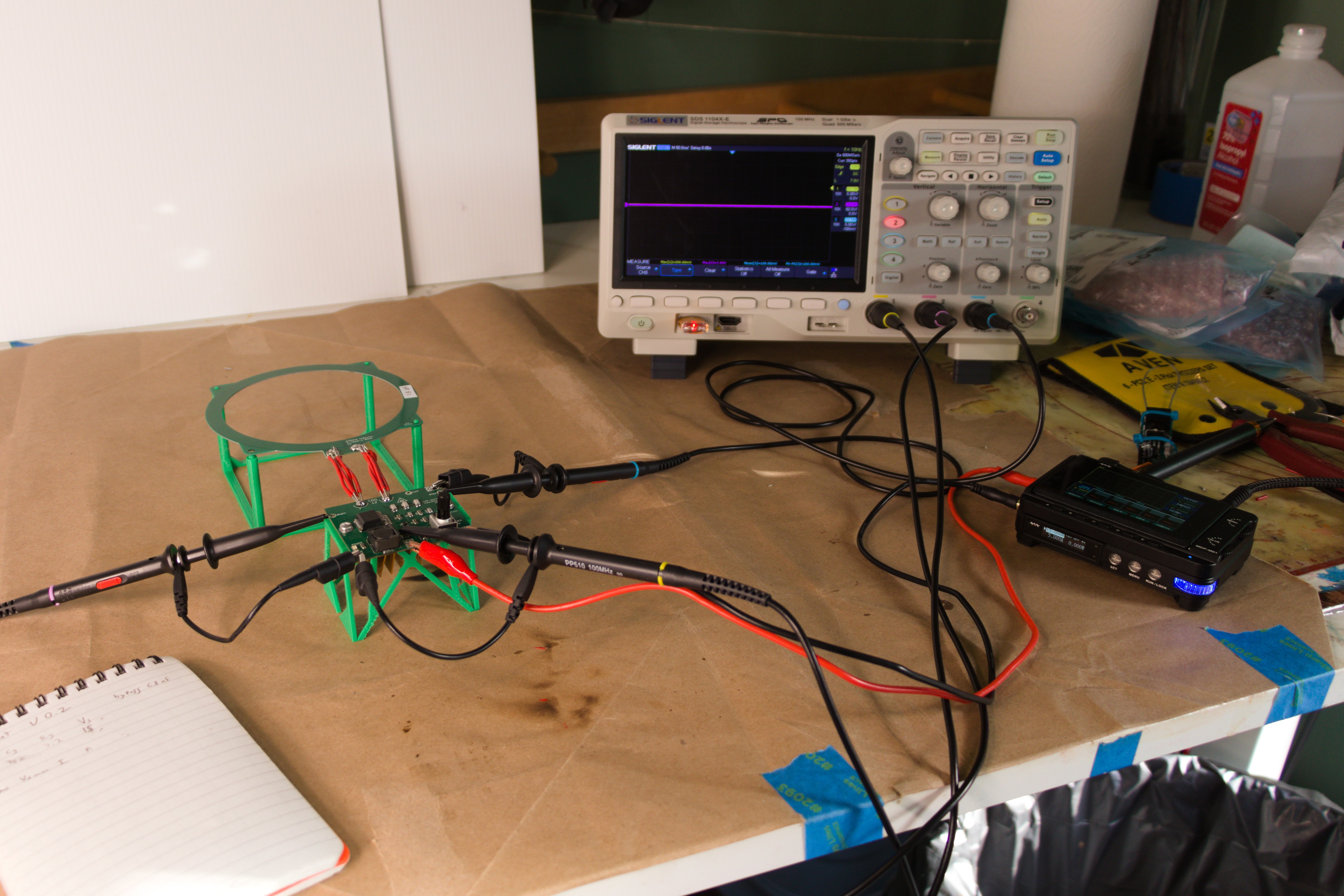
02/25/2024 at 21:36 • 0 commentsSpent a big chunk of the weekend adjusting a variety of component values.
![]()
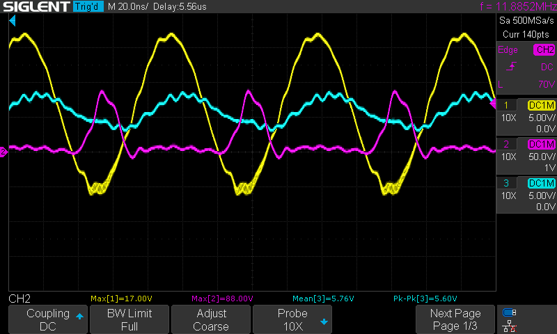
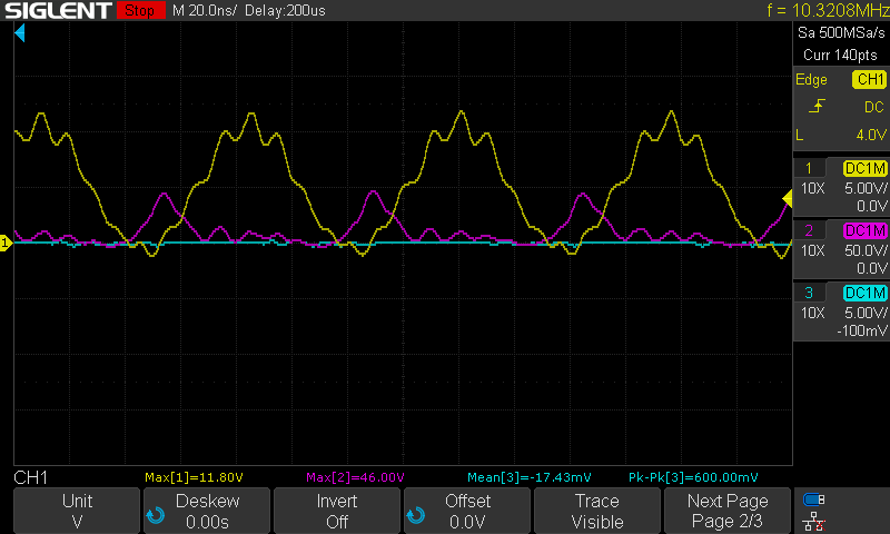
Here's the waveforms with the circuit unloaded (no toroid), at 18V supply:![]()
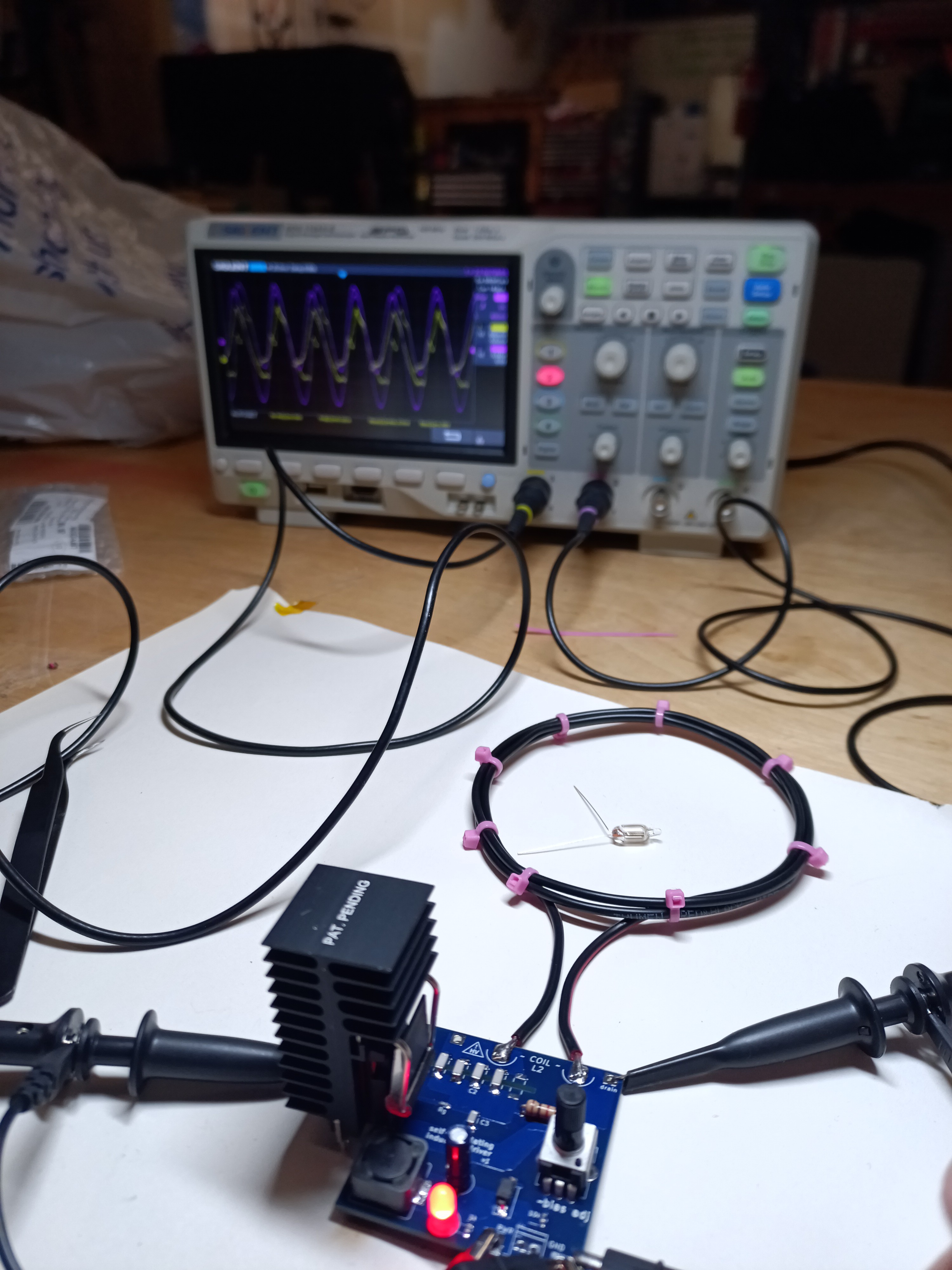
Yellow is Gate (5V/div), purple is Drain (50V/div), blue is feedback network bias input at TP5 (5V/div).
Looks decently healthy to me. I suspect that the gate protection zener diode is doing its job and helping to keep drive voltages within operational limits.
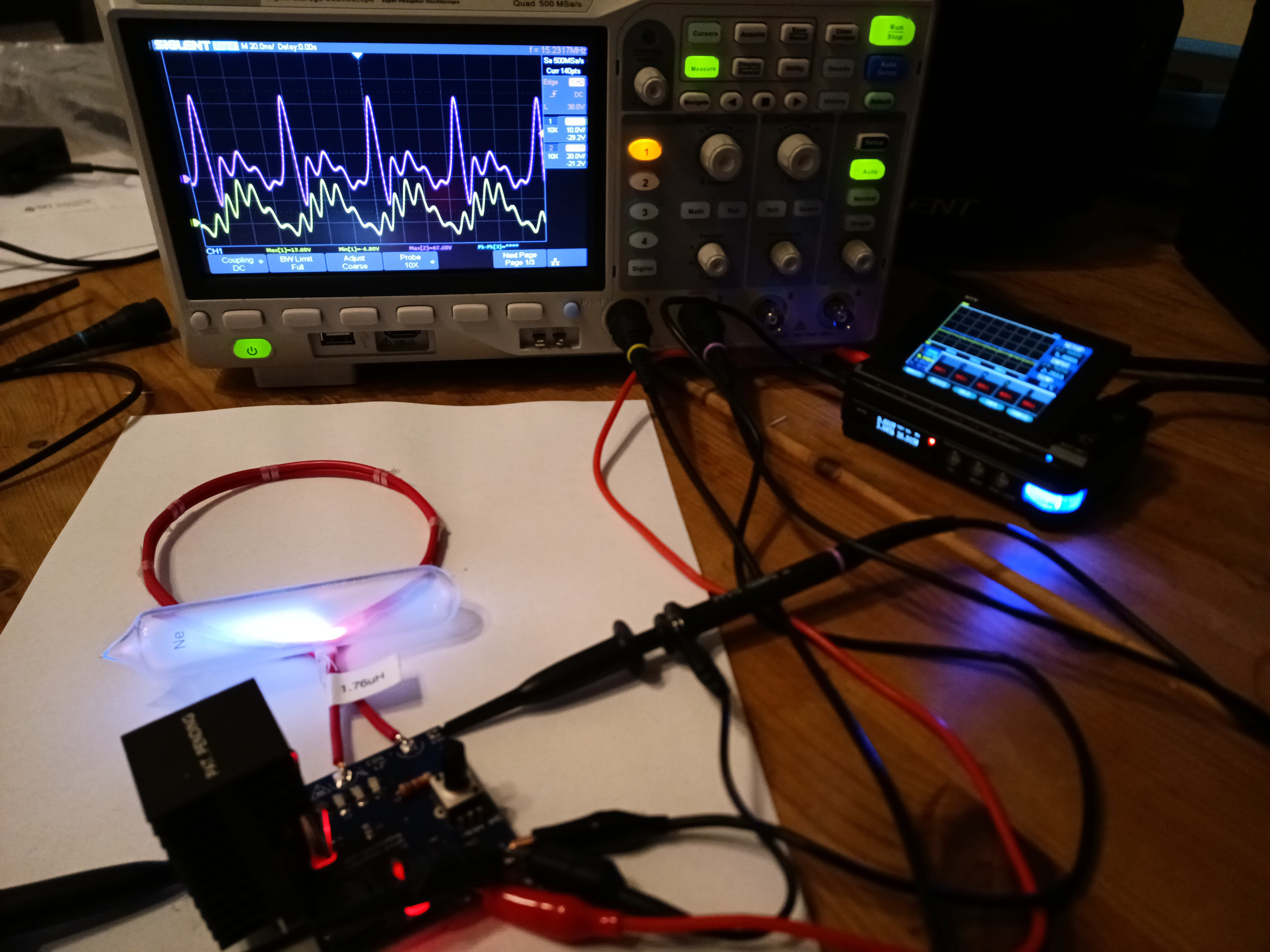
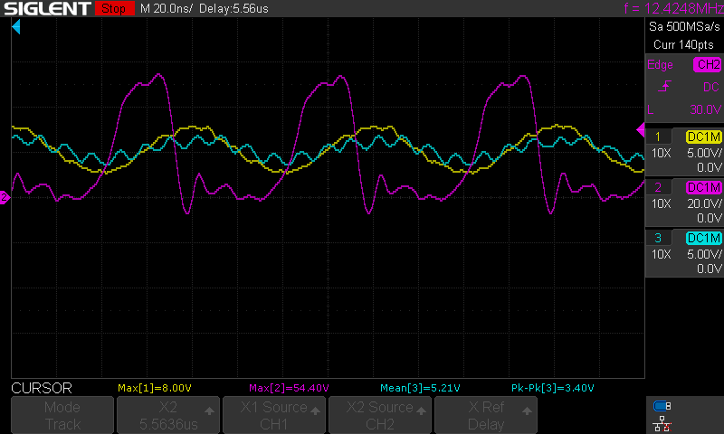
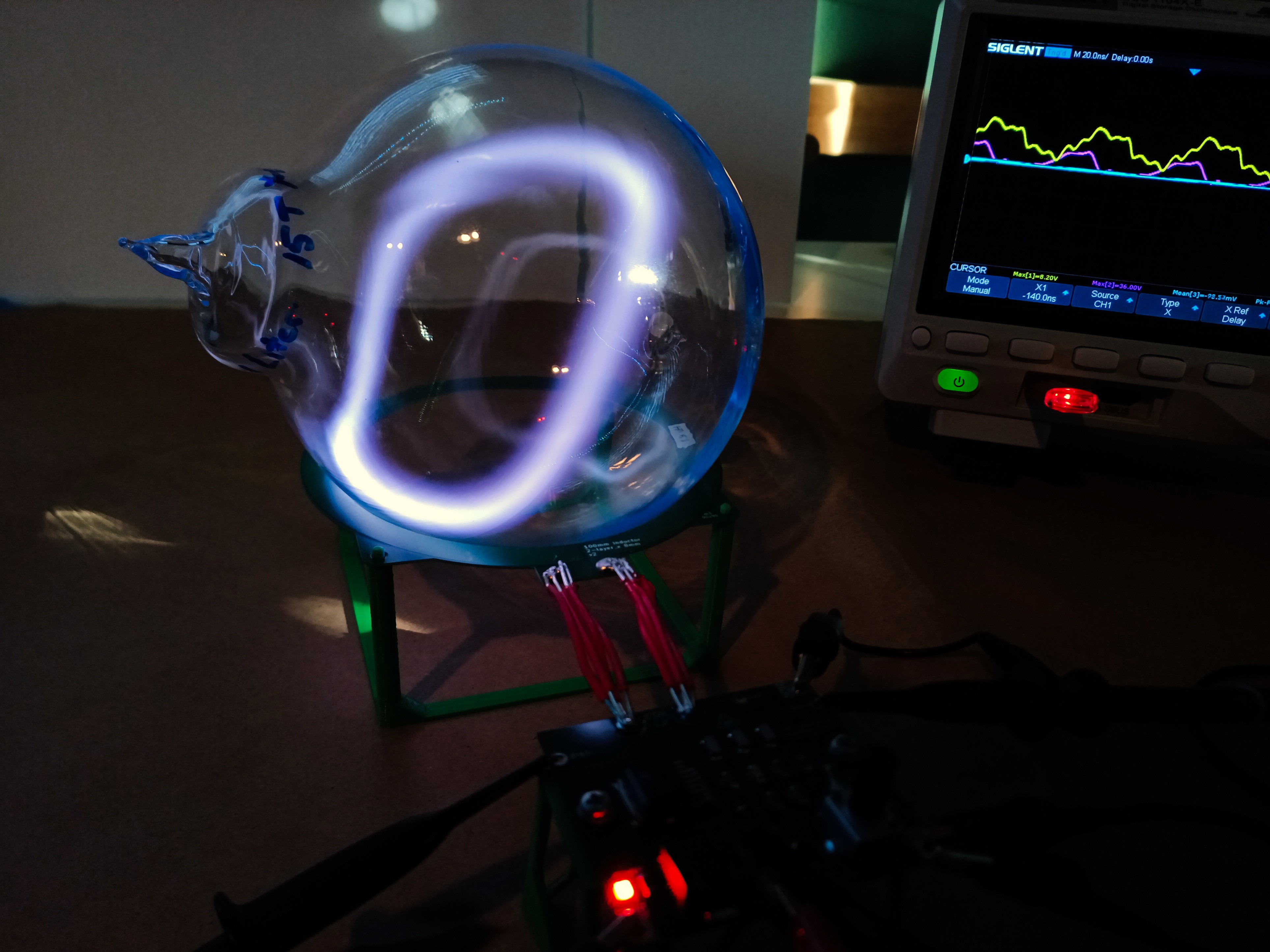
Here's the traces when the xenon is fully toroid-ing:![]()
Hm. Clearly the device is overall functional but these waveforms aren't as clean as I'd prefer. Maybe it's fine? [EDIT: as before, turned out a lot of the wiggliness was from bad probing. Shorten those ground connections!]
All right, so let's walk through the component changes. I'll spare the step-by-step of each individual test -- most of it was poorly documented and I was going for more of a "better or worse?" approach than robust characterization.
First off, primary tank capacitance was increased 99pF to 141pF. This was the first change made, as planned in previous project log "i would like my circuit to not cook myself".
Increasing capacitor value was broadly successful -- overall power draw was reduced to ~2.9 - 3.2A depending on circuit configuration. Yay!
Decoupling cap C4 was removed because it caused some kind of runaway oscillation on both gate voltage and power draw. A different cap value might be fine but for the moment, the pads are empty. [EDIT: the problem was that a cap here caused input power to ramp up faster than supply power could keep up with. The solution was more bulk input capacitance!]
I spent quite a while trying to increase operating gate drive voltages. You can see in the second pic that gate drive peak is only 8V, when I'd have preferred something closer to 15. My understanding is that MOSFETS really prefer to be driven by a square wave rather than this sinusoidal feedback. With intermediate voltages near the switching threshold the mosfet is in a state of "kinda-on", which causes a lot more power loss (and thus heat) than being fully on or fully off.
I was hoping that larger values of R2 would strengthen gate drive and increase the differential between the gate voltage and the (still too wiggly for my taste) bias voltage. Initially I spec'd R2 for 10k in this iteration, but it turned out that overly large values resulted in too tenuous of a ground reference. The max stable value I tested was 3.3k for R2.Similarly, decreasing gate capacitor C3 to 6.8nF increases gate drive voltage a bit, but it's not as dramatic a difference as I'd have expected.
Playing with the gate resistor Rg was a bit odd. Looking at the traces I saw very little change with values ranging from zero ohm to 10Ω. Subjectively, 0Ω seemed to cause the least heating of the mosfet, but I wasn't taking rigorous enough measurements to say that with certainty. (Also, the 10Ω resistor almost immediately toasted itself; the gate capacitance is slurping far more power than a little 1206 smd can handle.) I wasn't able to observe any kind of difference in probable turn-on delay based on scope measurements.
Looking back at the drain traces in the toroid-loaded condition, I see a couple of things:
- Drain voltage peaks at only 55-65V or so.
- Drain ringing after turn-on, including temporarily shooting negative.
I don't even know if either of those is even really a problem. I may investigate using a higher inductance feed coil L1 -- other folks describe 10uH, I'm only using 2.2k. Might also look into a schottky diode across the mosfet to clamp drain against going negative.
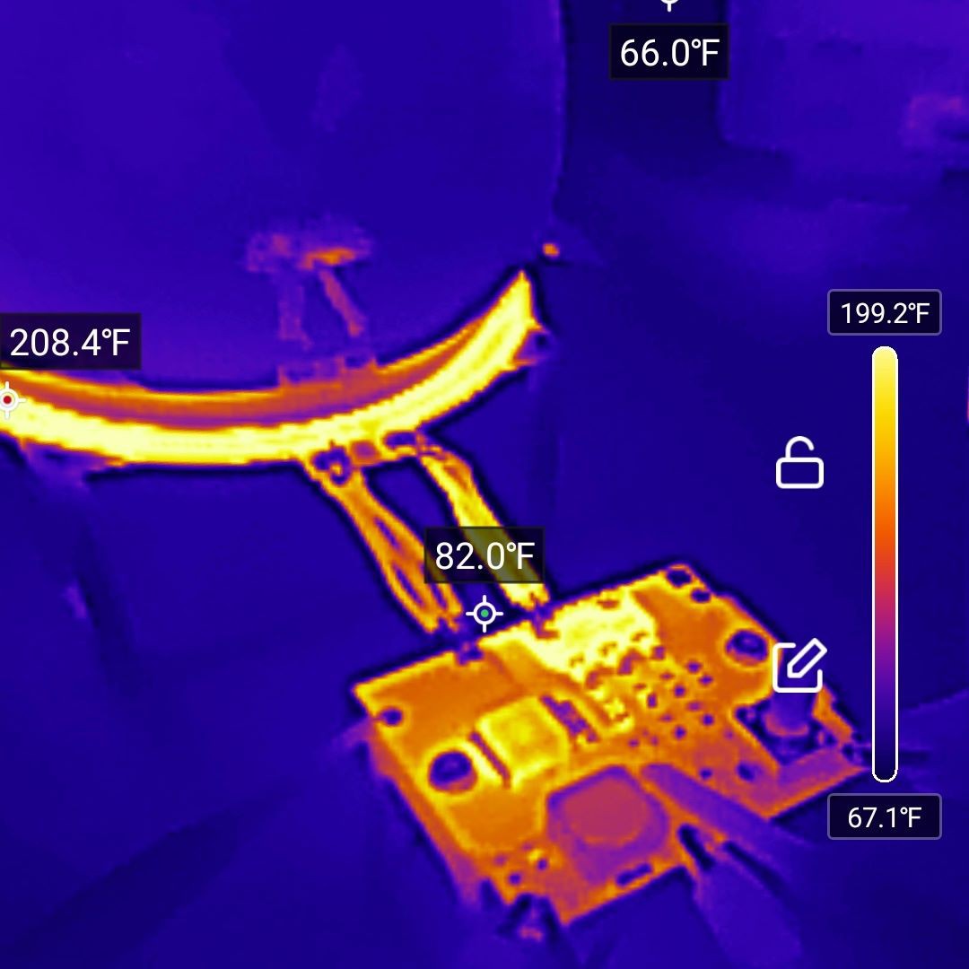
Returning to the topic of board thermals:
The key discovery was that heating on the inductor coil and the primary capacitor bank goes way
down when the xenon is actually ionized toroidal. I believe this lends some credence to the idea of framing coil heating in terms of "input energy has to go somewhere".
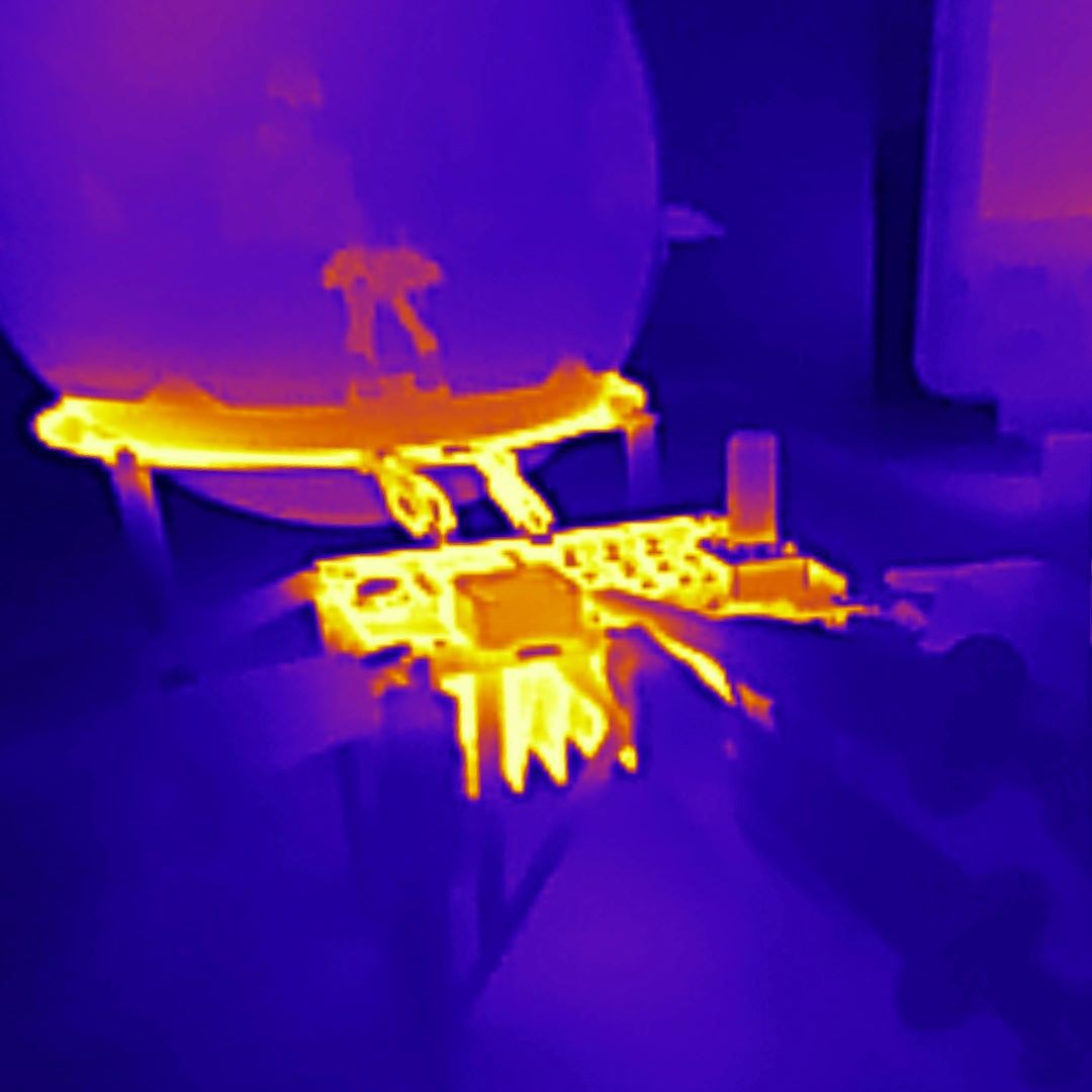
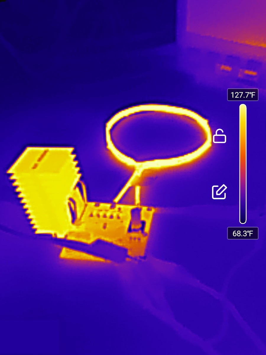
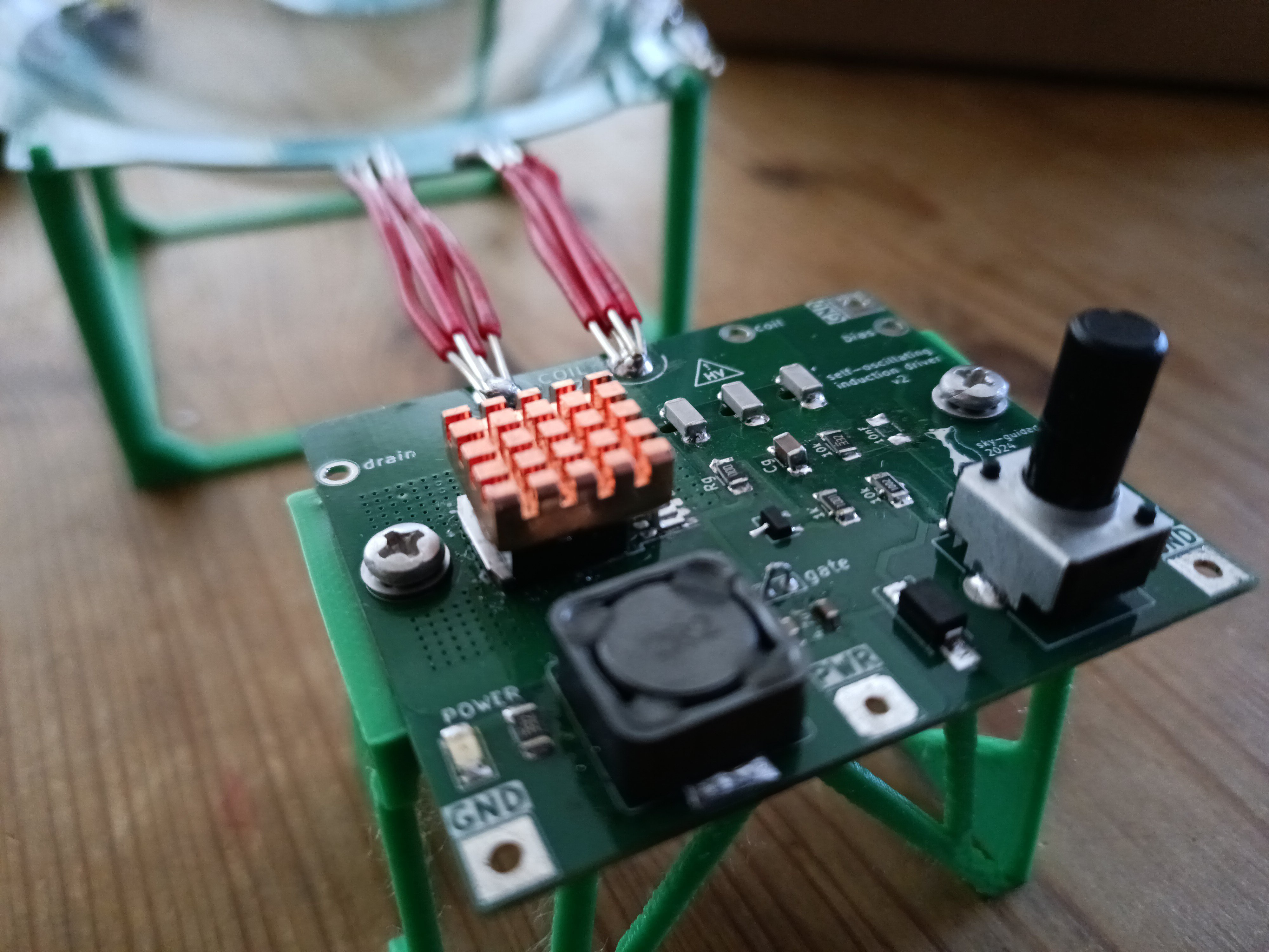
I also hooked up a little 40mm axial fan and aimed it at the board heatsink, and stuck a teeny copper heatsink on top of the mosfet.![]() With all of the changes, I was able to get temperatures to stabilize at ~100-110C on the mosfet body and ~50-60C on the coil while the toroid was active.
With all of the changes, I was able to get temperatures to stabilize at ~100-110C on the mosfet body and ~50-60C on the coil while the toroid was active.![]() That's hotter than I'd like, but... basically fine. It means that at the moment I can run the device for minutes at a time without worrying about it bursting into flames. Still probably worthwhile to use coil with wider traces, use more capacitors in the primary bank to spread out the load a bit, try to reduce mosfet losses, etc. Again though, yay!
That's hotter than I'd like, but... basically fine. It means that at the moment I can run the device for minutes at a time without worrying about it bursting into flames. Still probably worthwhile to use coil with wider traces, use more capacitors in the primary bank to spread out the load a bit, try to reduce mosfet losses, etc. Again though, yay!Stay tuned for more!
-
#3: i would like my circuit to not cook itself
02/16/2024 at 03:22 • 0 commentsFirst Light accomplished. What did I learn?
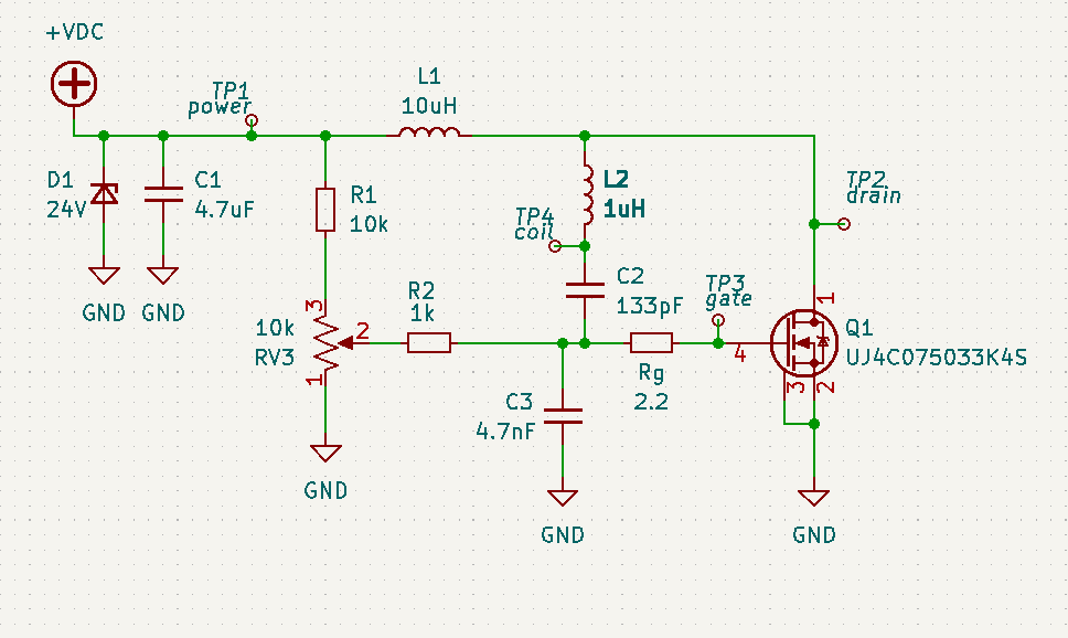
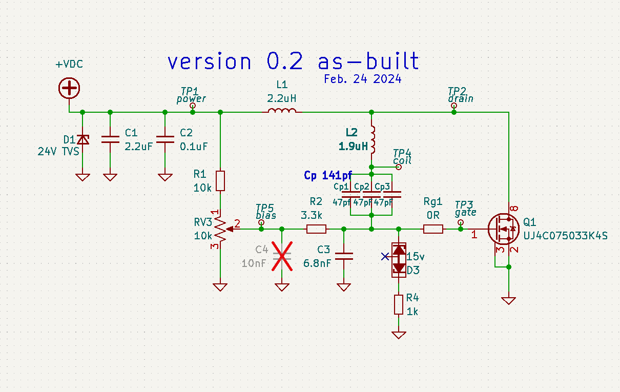
The circuit in its current iteration,
1: gets hot alarmingly quickly
2: is trying to draw more power than I can actually supply.
Those seem related, yeah.![]()
apologies for the excessively american temperature units
Based on simulating the circuit in the condition tested, at 15 volts supply I'd expect to see something like 50W power draw, at around 3.5A. The tests discussed in the previous post sure looked like the USB-based bench supply was badly voltage sagging, so the next day I hooked up the beefier bench supply -- and very quickly started sagging, then blew another mosfet. I suspect that this very-budget bench supply has some sort of destructively un-graceful switch from constant-voltage to the constant-current mode it failovers to when it hits 5A, but it's also entirely possible that the mosfet blew first and I saw the power supply feeding a shorted chip.
My power budget is <5A @20V (the 100-watt maximum of USB-C-PD), but I'd prefer to stay <60W if possible.---------- more ----------
If I simulate a lower primary capacitance (e.g. 66pF instead of the as-built 99pF), power draw is dramatically greater and the higher resonating frequency is also a closer match to what I observed on the bench. Same thing if I sim a lower inductance value. (This relationship of LC values and frequency is of course exactly what you'd expect just from looking at the series LC equation, but the effects on power I hadn't thought ahead to anticipate.) Based on the cap data sheets I wouldn't expect a huge de-rating but who knows. It's also possible there was error in measuring inductance values -- I don't have an LCR meter, so I set up a little parallel LC circuit that I drove with a square wave and o-scoped the resultant ringing.
Takeaway: I can likely offset observed power-hungriness with either a higher-value capacitor bank or primary inductor.
Adding more capacitance is pretty easy, so that's my next step. I may also investigate making a four-turn PCB inductor, but I'd prefer the wide open traces of the two-turn (plus two-turn make it easier to route traces for the ionization pilot arc, which is a topic for future discussion).
On the topic of the PCB inductor getting super hot: based on sims I expected ~10 peak amps in the primary inductor, or maybe 12A at the very worst. PCB trace width calculators using IPC-2221 or -2152 thermal design guidelines predicted temperature rises of <30°C. I observed temperatures shooting past 130°C within about thirty seconds. Either I'm getting quite a bit more current than expected, or the thermal design formulae don't apply here.
If I plug numbers into the SaturnPCB Toolkit -- a load current of ten amps, an 8mm x 600mm 1-oz trace, and a frequency of 13MHz -- it tells me to expect a power dissipation of about 3.2 watts. One thing the formula doesn't consider is that the inductor coil has two conductors stacked on top of each other. I also notice the toolkit is only estimated 0.02Ω DC resistance, so of course if I scientific wild-ass guess an actual resistance of 0.2Ω I'd expect ten times as much heating. That's a better match for my sensibilities for how immediately cookin' things got.
On a more fundamental level though, if the device is overall drawing 50-60W, that energy clearly has to go somewhere. Physically I'm not sure where I should expect the balance of energy to go. There's gotta to be some combination of circuit waste heat, energy delivered to the plasma, and energy emitted as legally-dubious radio waves. I'd hoped that the latter two would be the majority, but that was based more on optimism than analysis.
In any case, I'm going to try to bring the overall power draw down first, then reevaluate where I'm at on the coil temperature. The few other examples I've seen of this project all use copper tube coils so it's always possible that a PCB coil just isn't viable, but I'm far from ready to give up.
The coil isn't the only thing heating up though! Reducing overall power might help, but there's more I can learn from the first v0.2 tests.
Managing heating in the capacitors can be addressed by adding more capacitors. If I use six caps instead of three, by the simple magic of P = I²R I should expect a quarter of the heating.
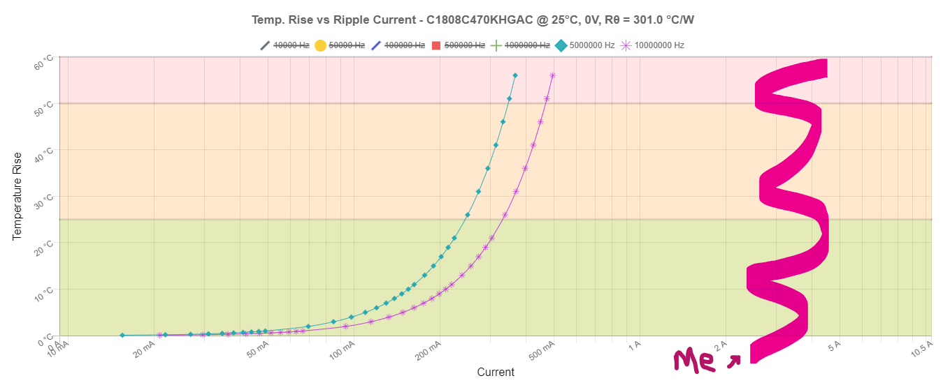
I couldn't find thermal specs for the TDK capacitors I've been using, but looking at Kemet design tool for the next-iteration caps, and, well![]()
Yeah that aint' great. 301C°/W feels a bit pessimistic but I don't have enough intuition yet to really know.
For the next board revision I can also consider dropping some thermal vias towards the heatsink underneath, and/or using SMD thermal jumpers to suck heat towards the ground plane.
On the topic of the heatsink -- based on the thermal cam it definitely looked like the heatsink was getting toasty, which is a good sign for it being decently well coupled to the mosfet. However, after thinking about it for more than five seconds I realized that I really ought to be keeping the heatsink cool because an already hot heatsink can't sink heat.
I knew that a fully-passively-cooled driver circuit was likely overambitious but I wanted to give it a go. Looks like I may have to install a fan (and possibly a bigger heatsink) anyway.Further experimentation will mean soldering on a new mosfet. That''ll require not only removing the heatsink, but also scraping off the phase-change thermal interface shmoo that's oozed all over the place only to squeeze into one thin layer for next tests. I've been putting that off for a few days, but it's gotta get done sometime.
Stay tuned, dear reader. -
#2: v0.2 -- First Light!
02/10/2024 at 02:41 • 0 commentsI'll put the cool part right up top: it works.
![]() (and i blew up zero mosfets in the process!)
(and i blew up zero mosfets in the process!)
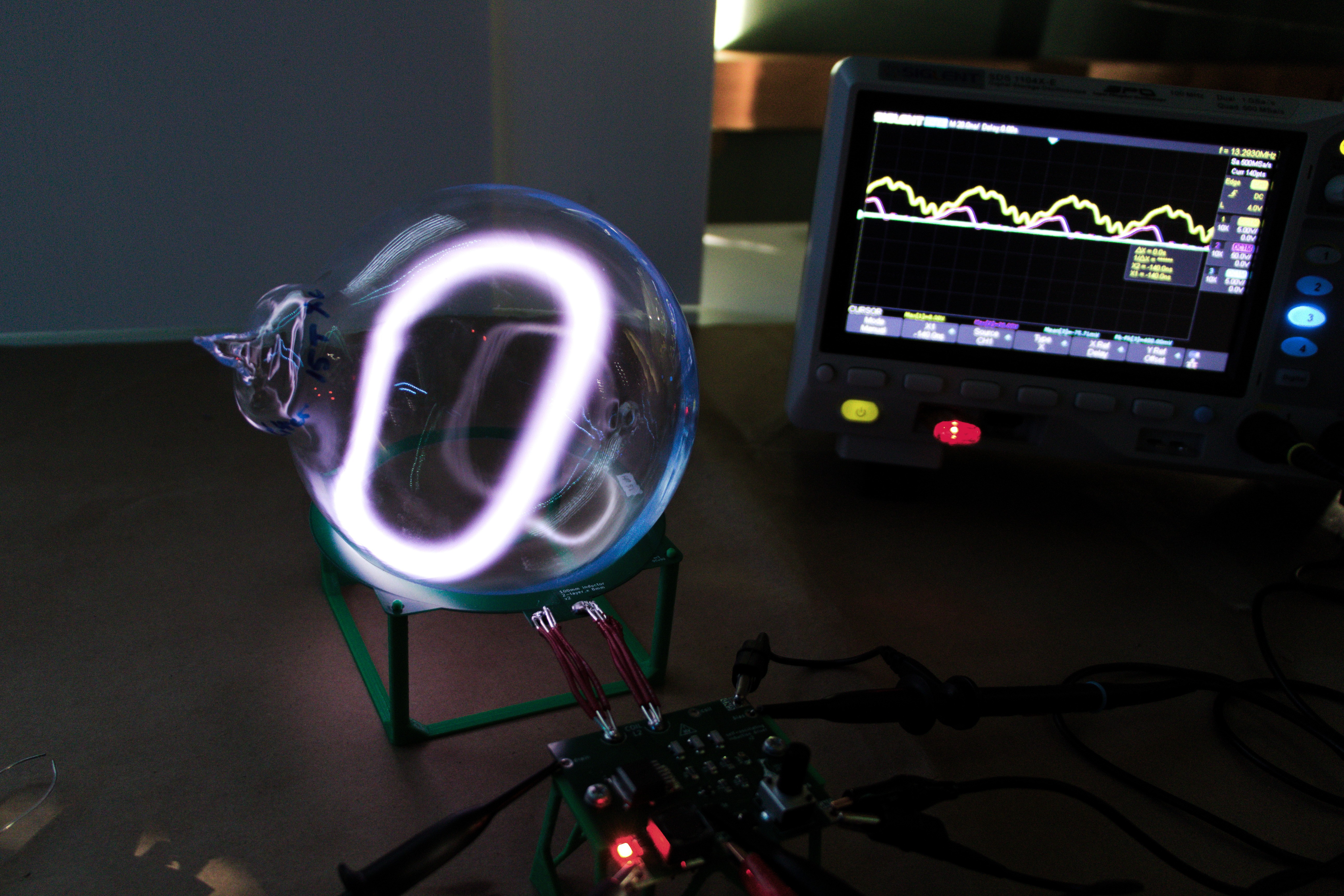
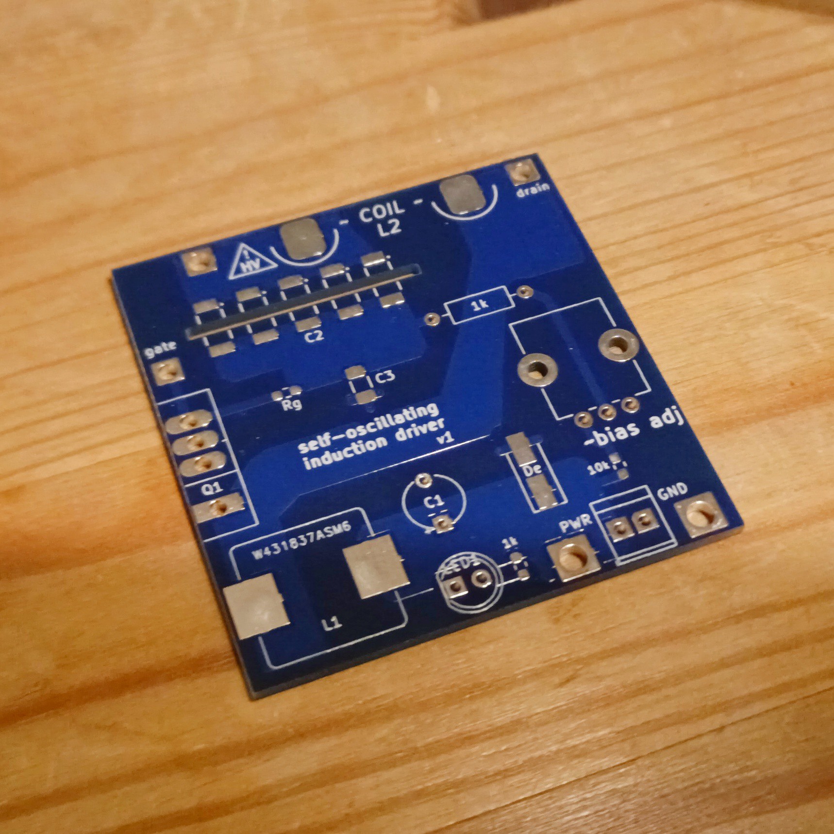
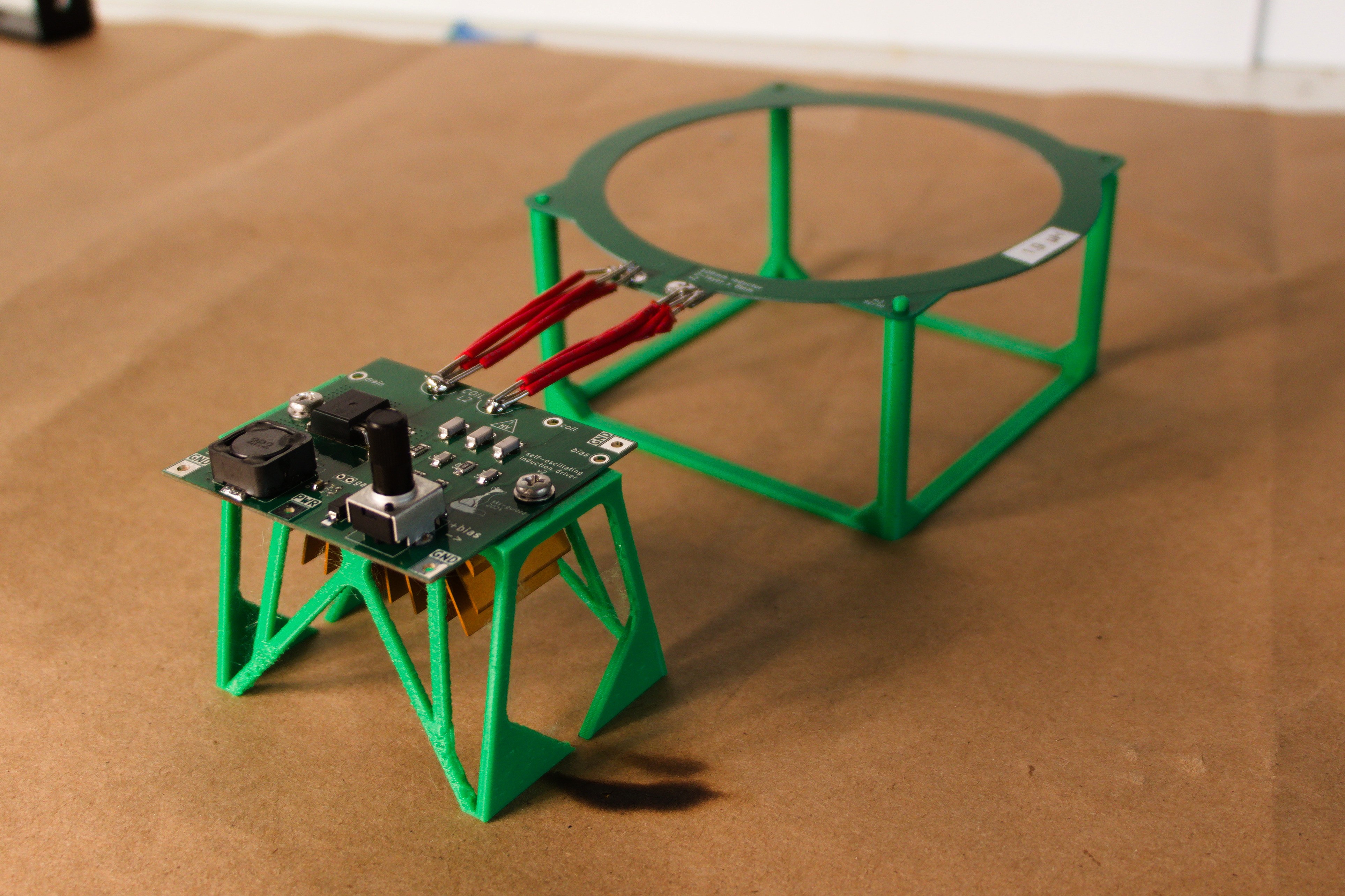
Version 0.2 boards arrived lookin' nice and spiffy.![]()
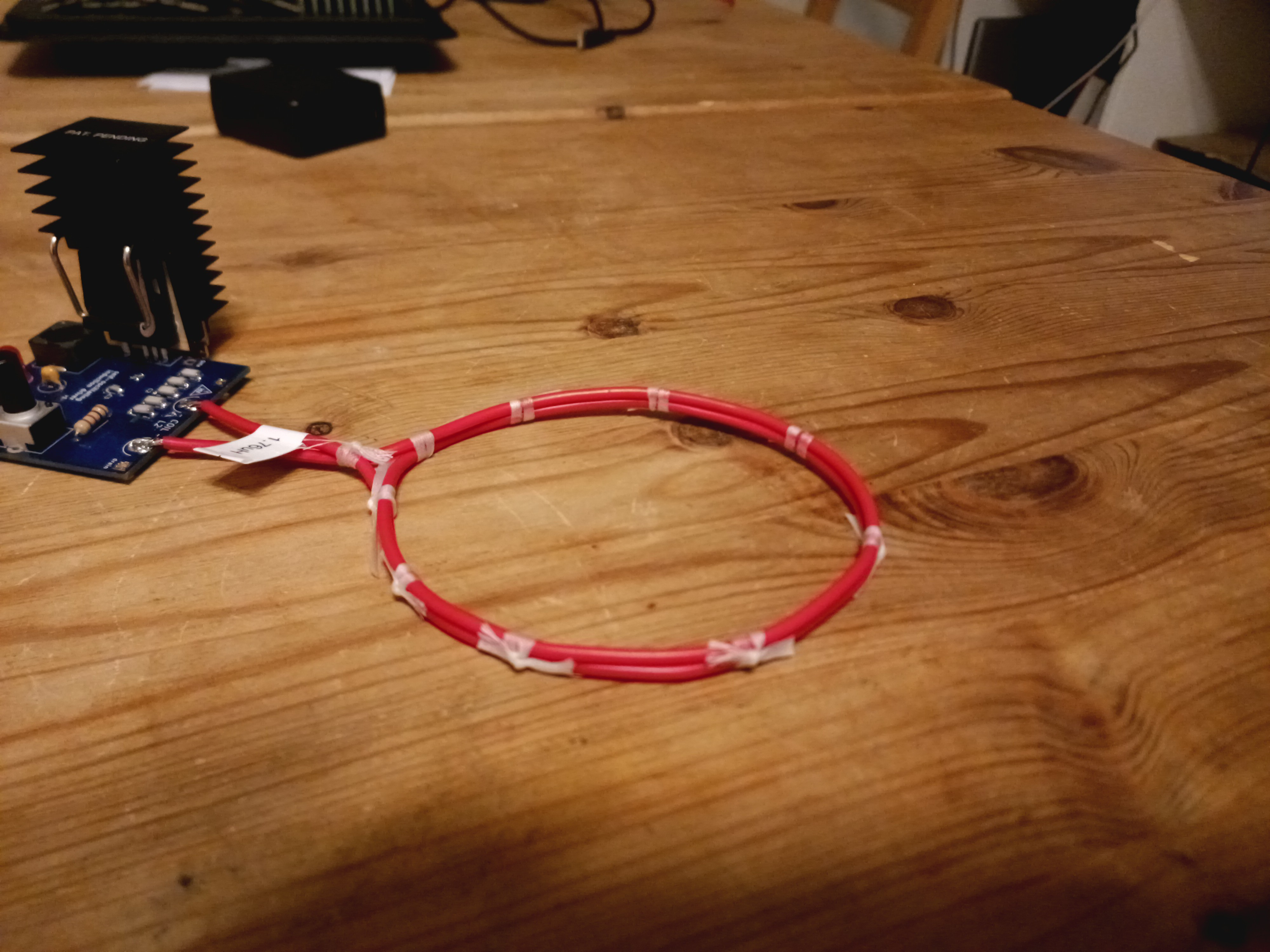
Everyone else I've seen who does a variant on this project uses a primary inductor made either of regular wire or copper tubing. I thought a PCB inductor would be more elegant. This inductor is two stacked turns on 0.6mm PCB, 100mm center span and 8mm wide. I measured the inductance to be about 1.9µH.
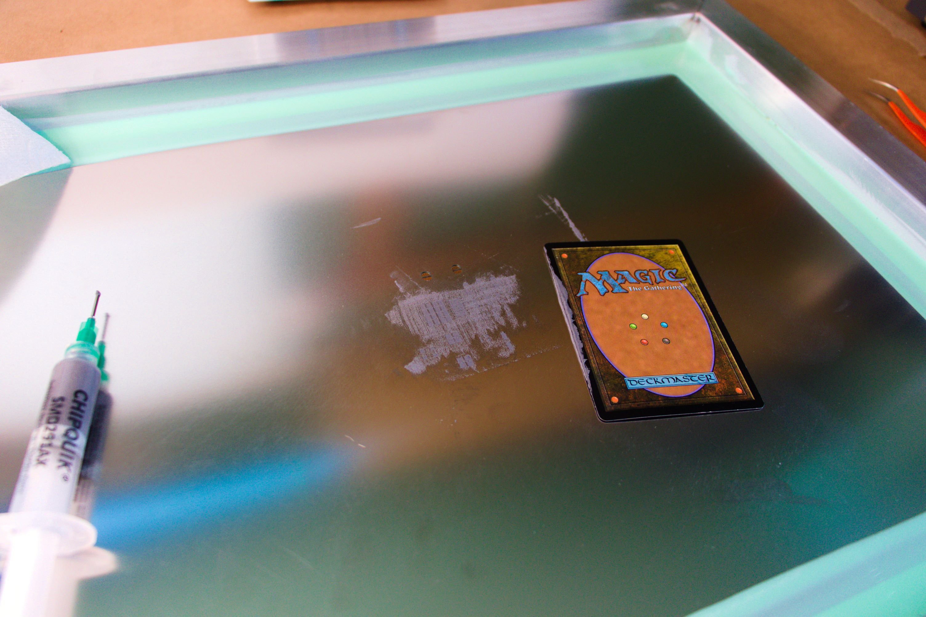
This was my first time using an actual solder stencil and hot-plate reflow rather than daubing on solder paste and using the hot air station. Turns out, using an actual stencil is way easier. Who'd have thought. Also turns out a scrap MTG card is a great paste spreader -- thanks to my gf for the improvised tool 🌈✨![]()
Soldered up beautifully.
![]()
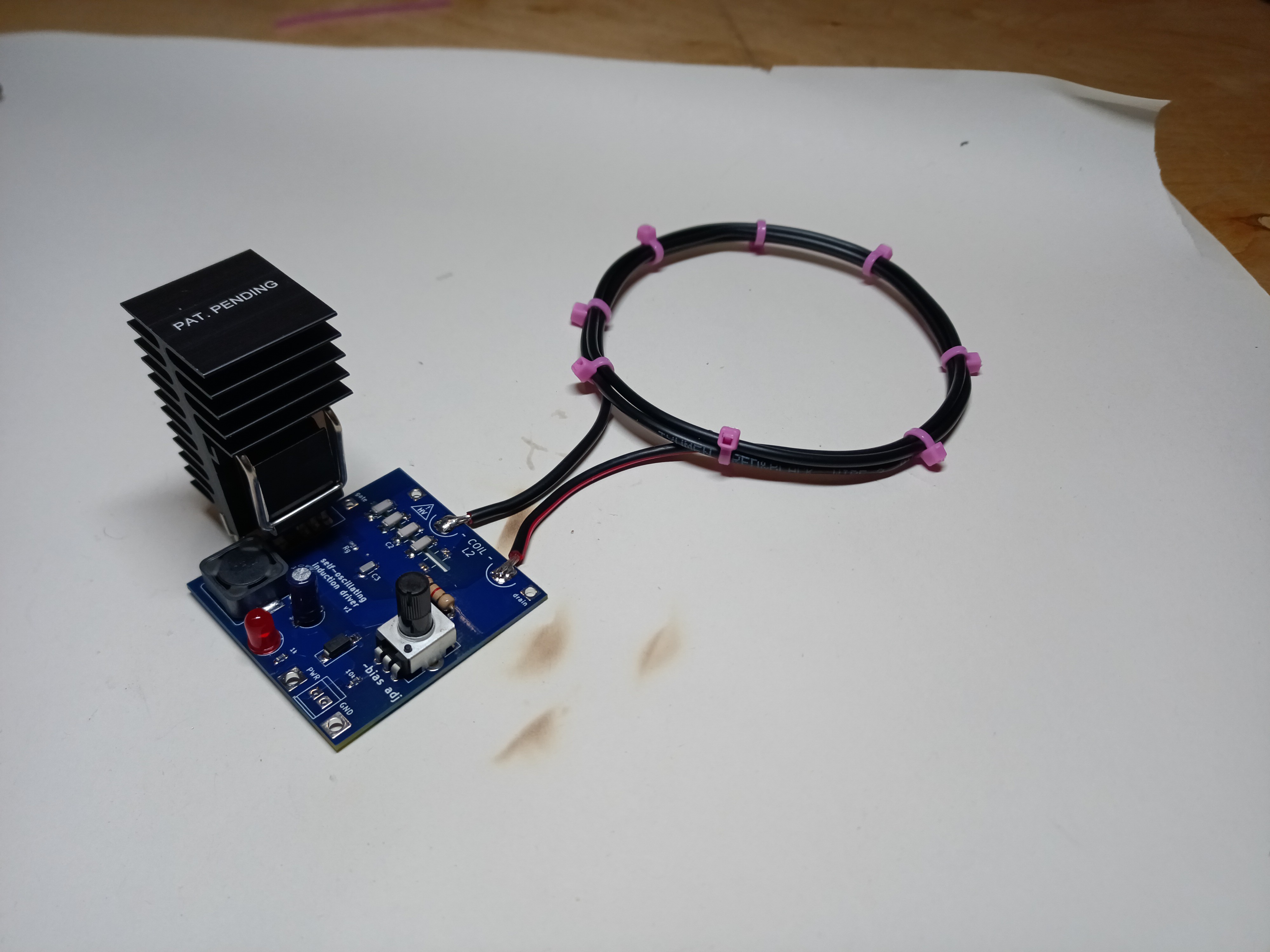
Since previous test coils had their 18ga wires badly overheat, I used bundles of 4x18ga to connect the board and test inductor. This is either a hacky kludge to get more surface cooling area, or a way of making bootleg litz wire -- take your pick.
---------- more ----------
Heatsinking for the mosfet is on the bottom side of the board -- you can see some of the orange fins peeking out. (There was an odd misadventure of the board flexing and making poor contact with the heatsink until I was able to melt down the kinda-thick phase-change thermal interface pad with the hot air station.)
I designed the board to use a duo of 0.1µF and 10µF capacitors for input power smoothing/decoupling... then realized during assembly that in my capacitor kit, those values aren't rated to enough voltage. 6.8nF was the highest value that fit in the 0603 footprint with a 50V rating. Fortunately the power input looked stable enough under load.![]()
I spent quite a while futzing with the circuit and adjusting components trying to track down what looked like self-oscillation. Turns out nah I was just being a silly goose; the potentiometer was upside-down relative to v0.1 and I'd been turning it the wrong way, in spite of having triple-checked during board layout and marking the orientation on the board.
![]()
Clearly still needs some tuning but this is the basic waveform I expected. Yellow trace is gate (5V/div), purple is Drain (50V/div). Interestingly I was able to get strong oscillations and a running toroid even at 12V supply, when BackMacSci talked about 18V being the minimum for his setup. I'm hoping that adjusting Rg will reduce some of that higher-frequency ringing. [EDIT: Turns out this was mostly poor probe technique!]
The PCB inductor still gets immediately and disconcertingly hot, even with much more dissipation area that the initial wire coil.![]() There's also distinctive heat buildup around the primary capacitors. Downsizing to a bank of three (from five) might have been asking a bit much.
There's also distinctive heat buildup around the primary capacitors. Downsizing to a bank of three (from five) might have been asking a bit much.
Good news is that the underside heatsink is indeed sinking heat. The mosfet gets hot quickly too, but I'm hoping better circuit tuning will help.![]()
Here's another photo of the toroid:
![]()
You can see that the o-scope waveform is all wonky when the toroid is actually toroid-ing.
For these tests, I was using a Miniware MDP-XP power supply. I'm a big fan of that tool -- it's tiny, usability is great. It also runs off of USB-PD, and in tracking down a variety of odd behaviors I ascertained that the USB power brick I was using may have been rated to 20V and 5A... but not both of those at the same time. Full load was causing substantial voltage sag.
Next tests: a beefier bench PSU. Stay tuned! -
#1: v0.1 -- the inevitable first prototype failure
02/04/2024 at 00:18 • 0 commentsWhipped up a prototype PCB in KiCAD, ordered a batch of parts from Digikey, all set to go, yeehaw.
![]()
(not pictured in the above schematic: power LED and some other board affordances.)
![]()
Of course I knew that this probably wouldn't work first-time, but I still held out hope.
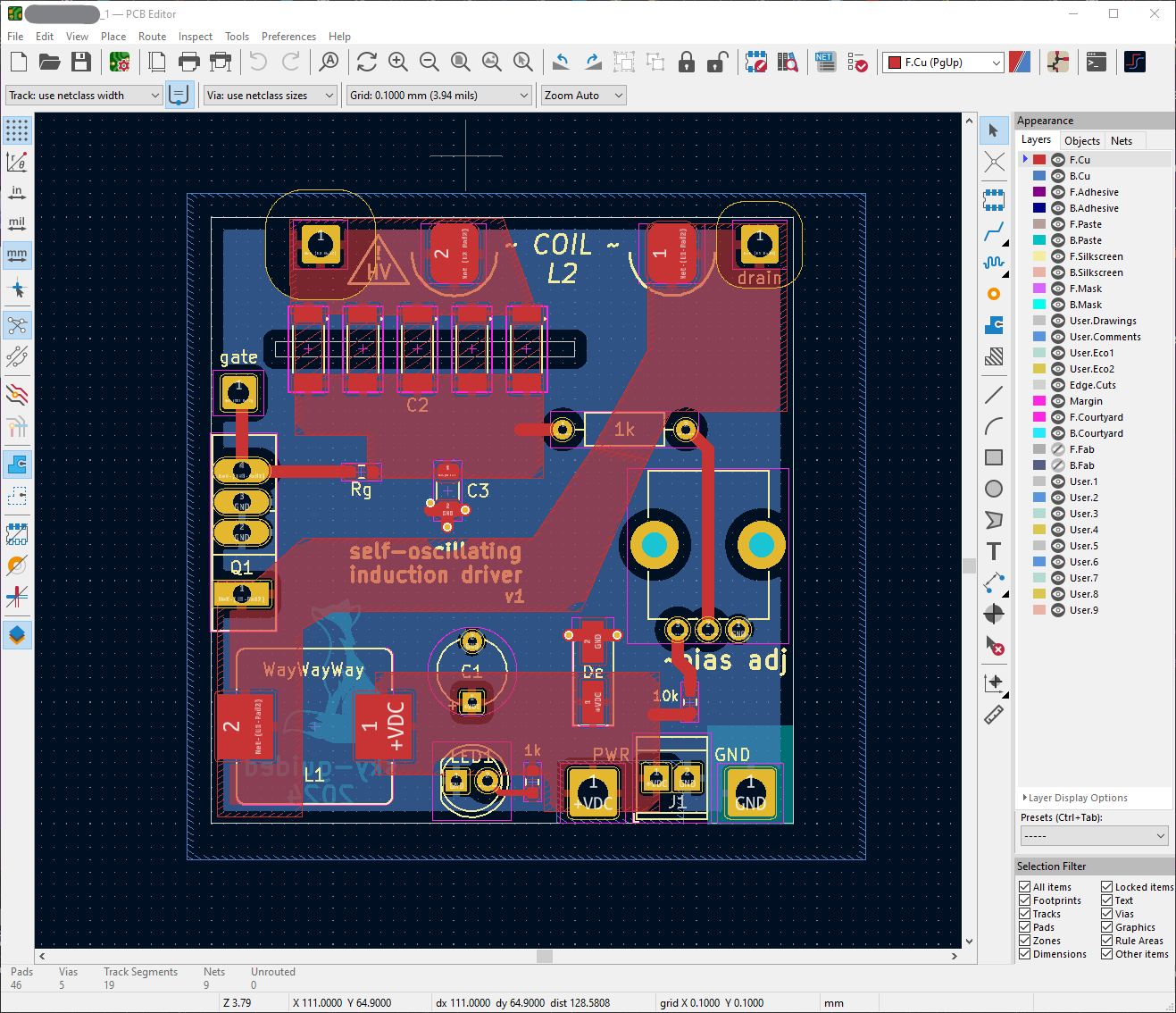
There's some ugly design compromises -- in particular, the 1k through-hole resistor is doing double-duty as a jumper wire. I increasingly prefer to prototype with surface mount parts whenever possible, but this board was an odd mix of SMD and THT. The bank of 5x capacitors (marked C2 on this board) was intended so I could easily adjust the total value of C(p) and to spread heating between multiple components.![]()
Decent boards, blurry photo.
![]()
Assembled easily enough. This first coil was three turns of 18ga wire.
![]()
Things got going with some kind of oscillation, but definitely not what I was looking for.
At this point I blew my first mosfet. The mosfets I'm using are the UJ4C0750-series new-hotness SiC FET's from Qorvo, and they're not particularly inexpensive. The THT mosfets used in this first prototype were also fairly annoying to replace, since the holes barely had enough clearance diameter and solder was hard to sufficiently clear out.![]()
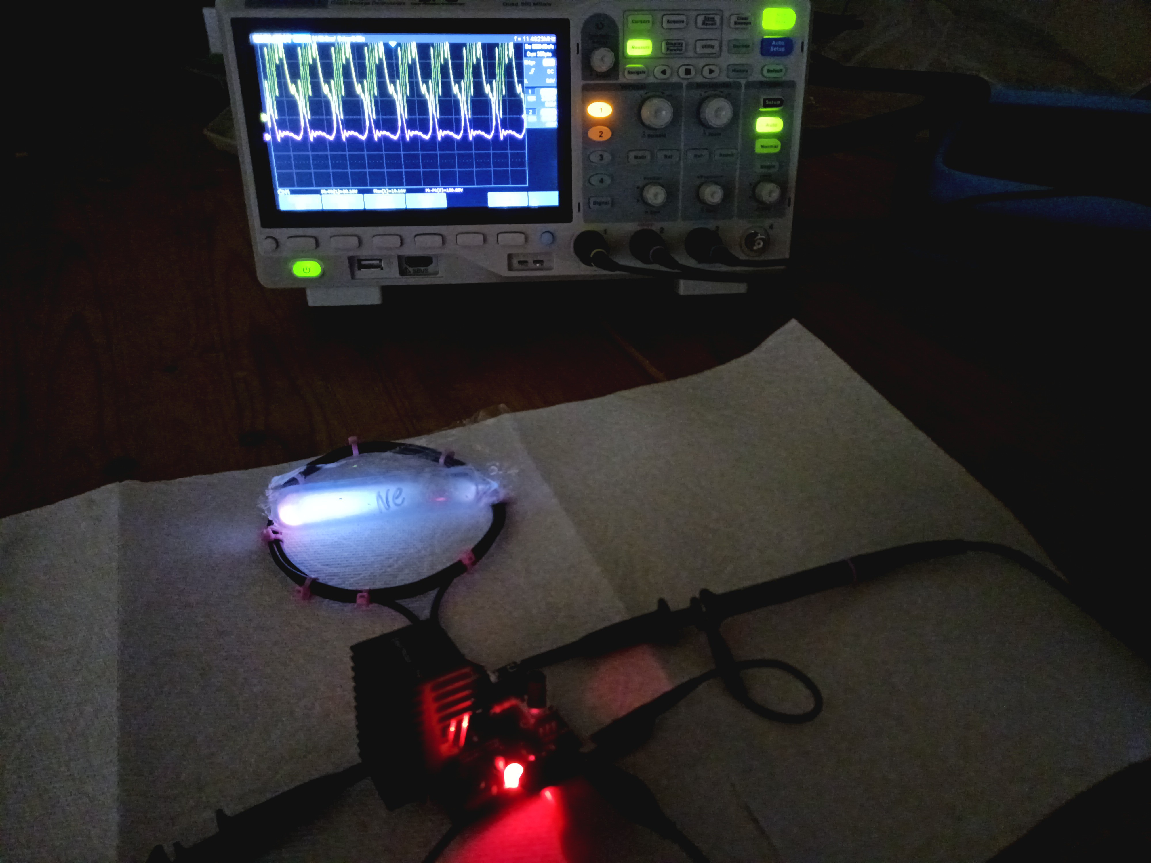
Changing C(g) from 22nF to 10nF (almost) got me the intended waveform! Since my 1L xenon globe from Wayne Strattman hadn't arrived yet, I was illuminating a small ampoule of neon.
There's clearly some kind of ripple on the gate (yellow trace). I measured that to be somewhere around 100MHz, but unfortunately I don't have good oscilloscope printouts for these first trials.
Blew up another mosfet when bending the coil while the circuit was running, and somehow blew up a third trying to probe the HV coil voltage (and possibly smoked an o-scope probe in the process -- really should have noted its voltage limit first). I'm guessing I got some kind of inductive kick at loss of oscillation?
A big deficiency in this first prototype is there's no voltage protection on the gate.![]()
Component and mosfet temperatures stayed pretty reasonable, but the coil got very hot very quickly. In retrospect the cause was obvious -- skin effect depth at these frequencies is only about 20 microns, and the top 20 microns of a 18ga insulated wire just isn't enough conductor.
I made two more inductors, this time actually characterizing their inductance. The first was a tight 1.3uH coil designed to wrap around one of the ampoules in the hope that I could see at least some inductively coupled plasma before my xenon globe arrived. LTspice said that inductance value should work fine, but instead my mosfet instantly failed short.![]()
A two-loop coil of ~1.8uH worked, but the switching is clearly messy (pictured here at 12V supply). The big motivator for investigating a two-loop coil was my intent of using a two-layer PCB as the inductor in my final design.
![]()
Using lacing tape does make the coil a lot nicer than zipties, at least. Lacing tape is great and I wish more folks knew about it.
And... I blew my last mosfets screwing around with different drive voltages and component values. RIP.
Version 0.2 is coming soon.
Plasma Toroid (sky-guided PCB edition)
inductively-coupled radiofrequency plasma toroid in xenon gas
 With all of the changes, I was able to get temperatures to stabilize at ~100-110C on the mosfet body and ~50-60C on the coil while the toroid was active.
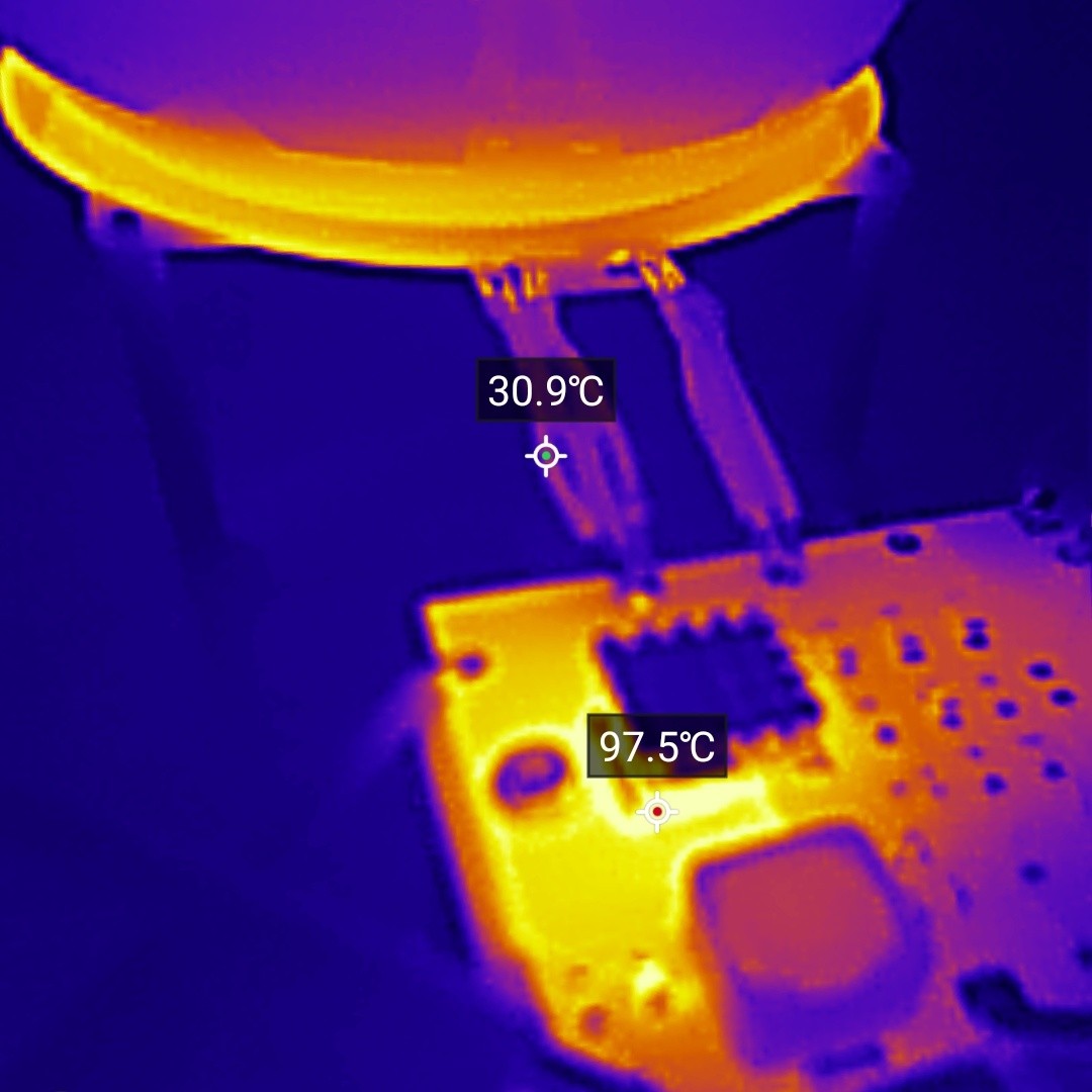 That's hotter than I'd like, but... basically fine. It means that at the moment I can run the device for minutes at a time without worrying about it bursting into flames. Still probably worthwhile to use coil with wider traces, use more capacitors in the primary bank to spread out the load a bit, try to reduce mosfet losses, etc. Again though, yay!
 (and i blew up zero mosfets in the process!)
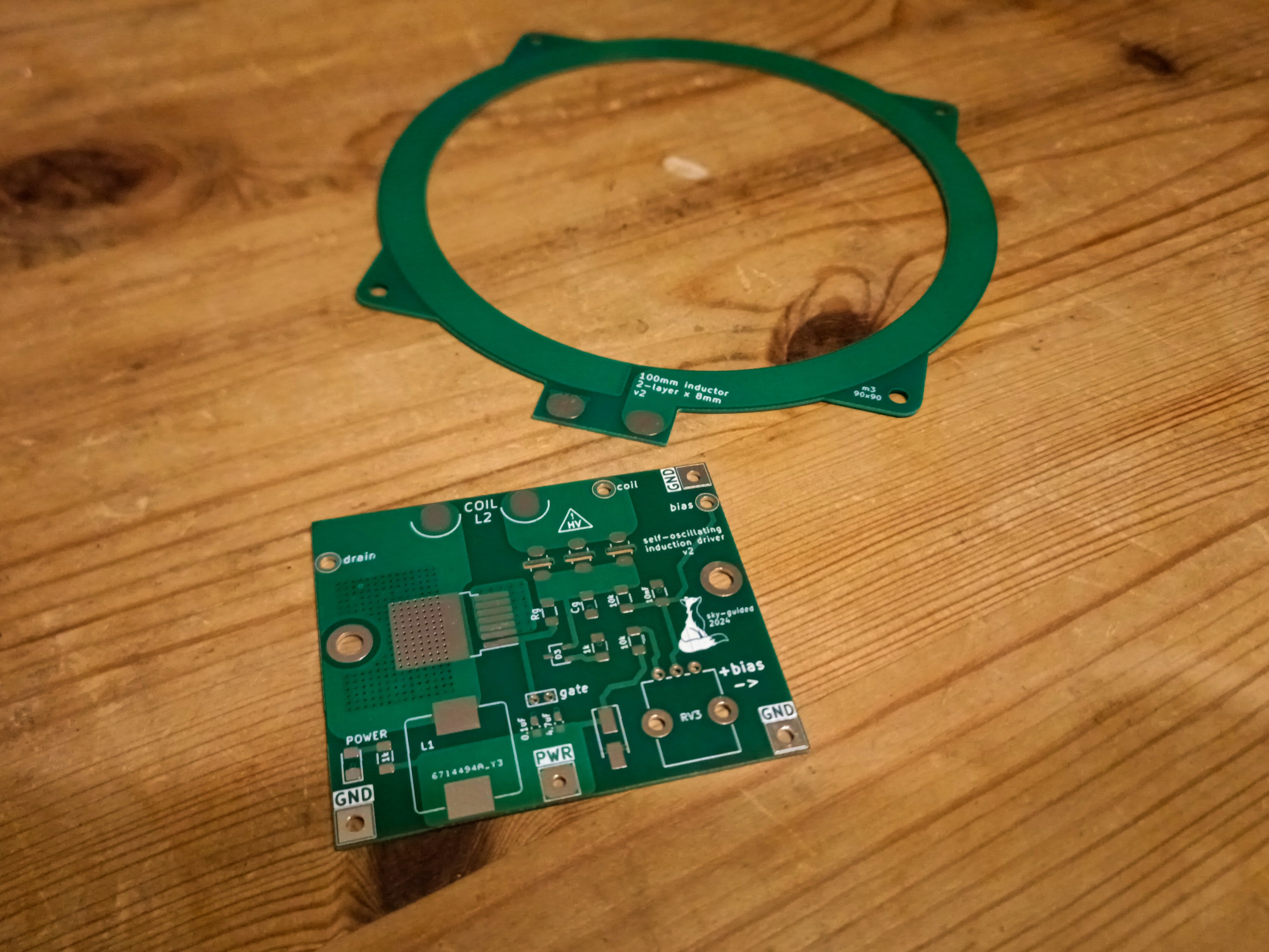
 There's also distinctive heat buildup around the primary capacitors. Downsizing to a bank of three (from five) might have been asking a bit much.