Jesse Farrell
====== Project Status ======
Schematic -------------------- ( ✓ )
PCB Layout ------------------ ( ✓ )
Documentation ------------- ( ✓ ) - See HAS
Order + Assemble --------- ( ✓ )
LAB: Sparkup ---------------- ( ✓ )
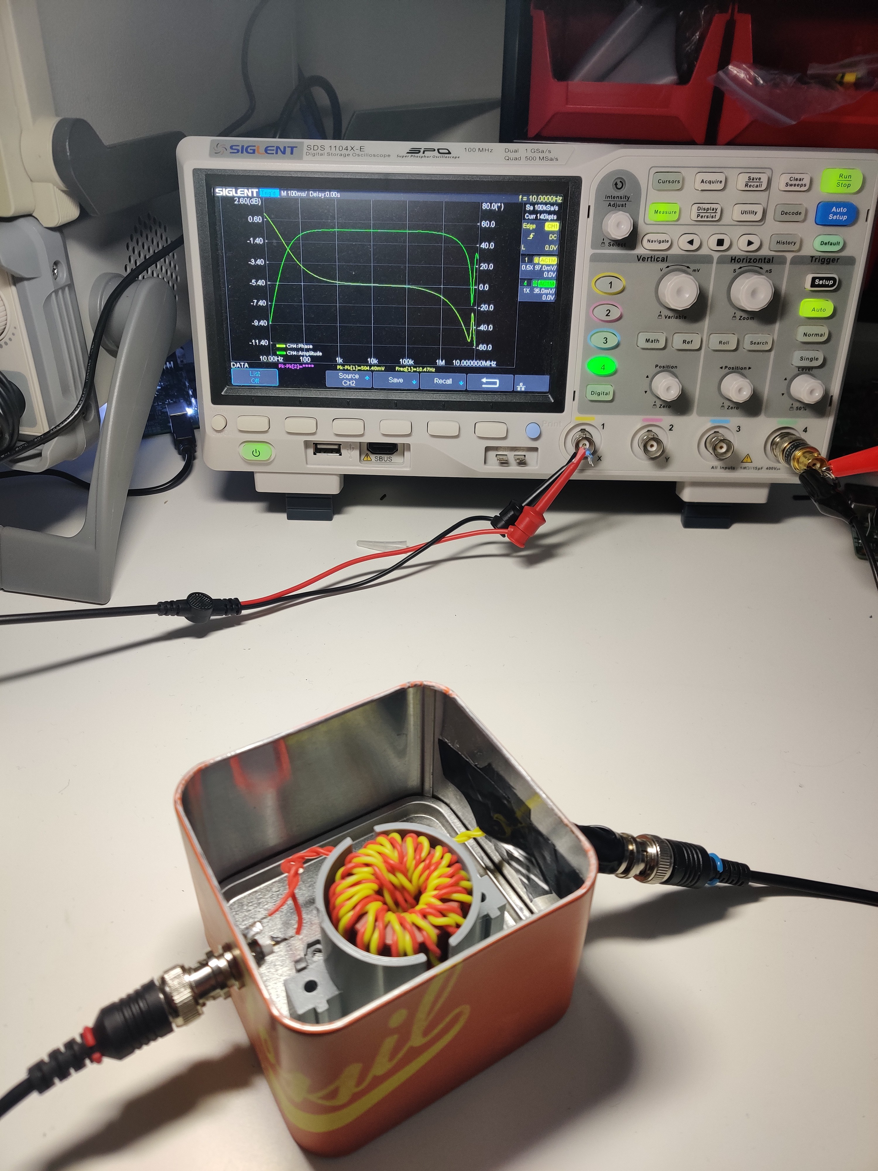
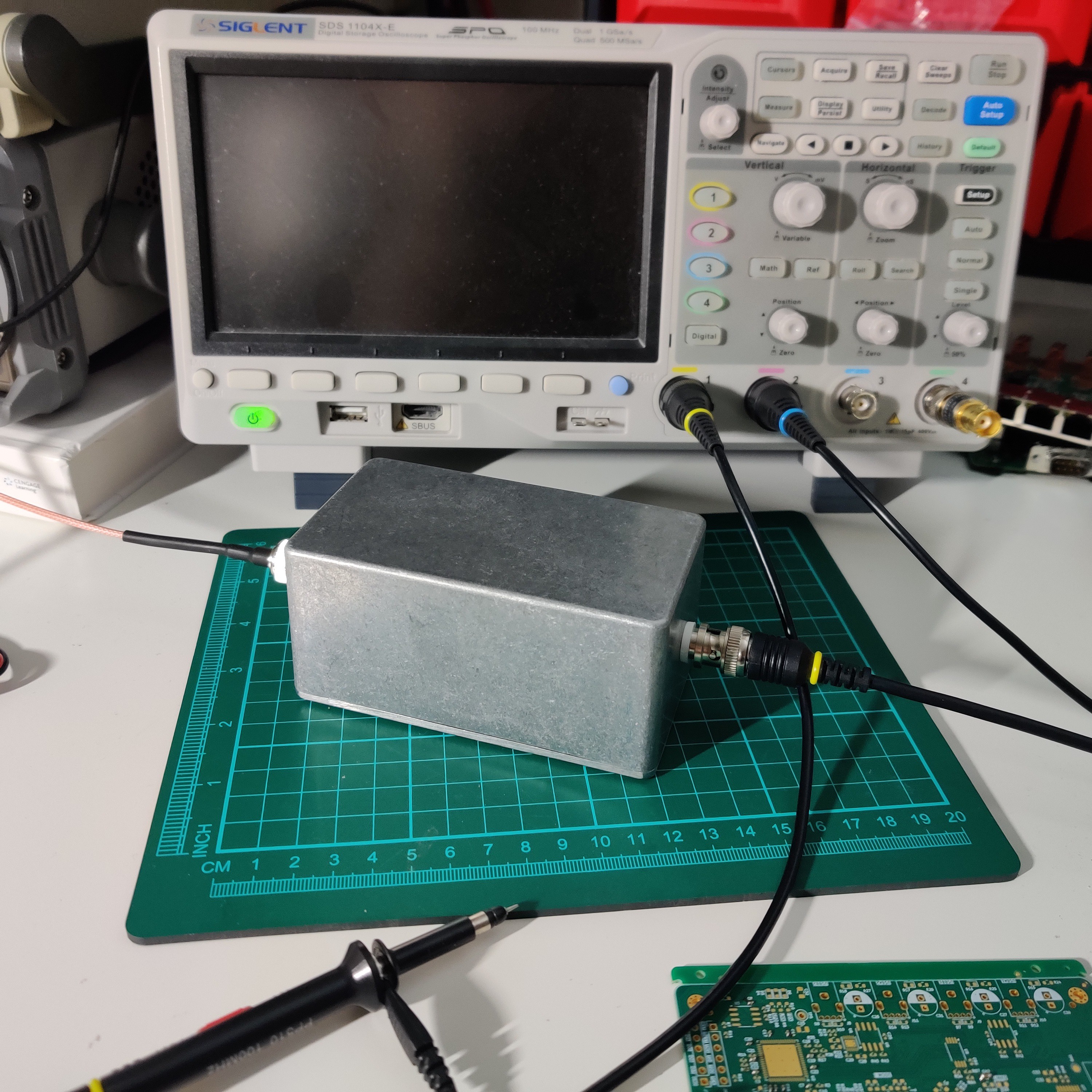
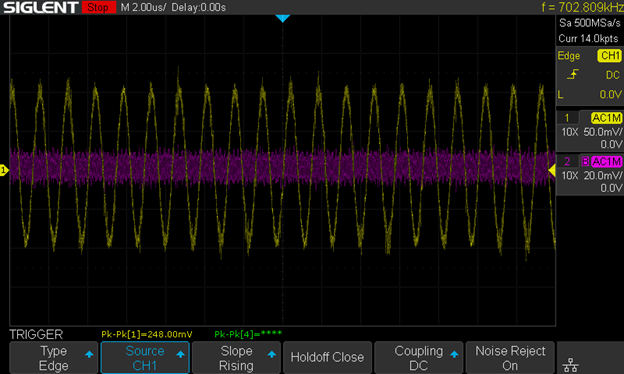
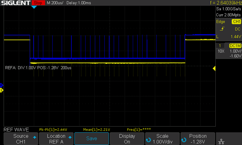
LAB: SI Analysis ------------- ( ✓ )
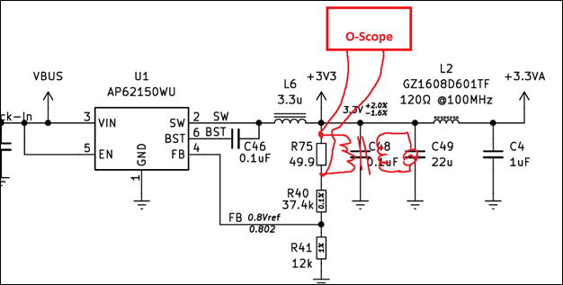
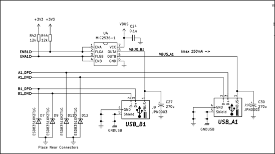
LAB: Power Analysis ------ ( ✓ )
Derisk Capacitive XFRM - ( ✓ )
====== REV 01 ======
Schematic Update --------- ( ✓ )
PCB Update ------------------ ( ✓ )
Order + Assemble --------- ( ✓ )
LAB: Sparkup ---------------- ( ✓ )
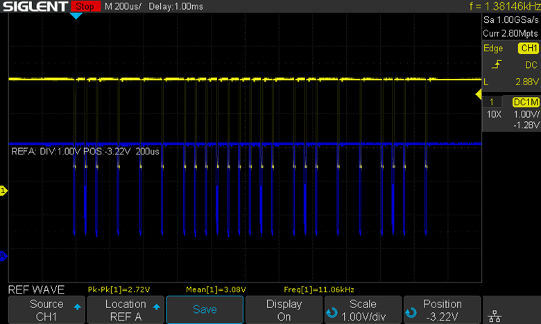
LAB: SI Analysis ------------- ( ✓ )
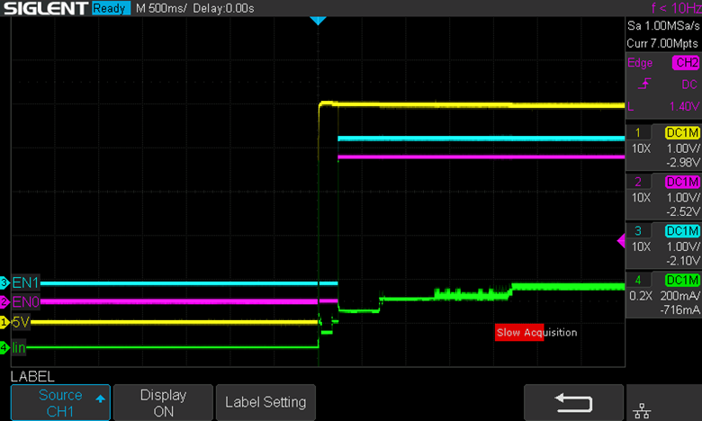
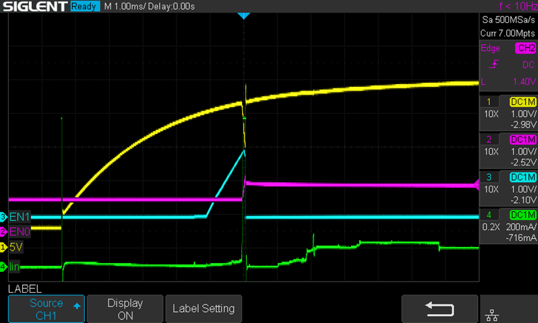
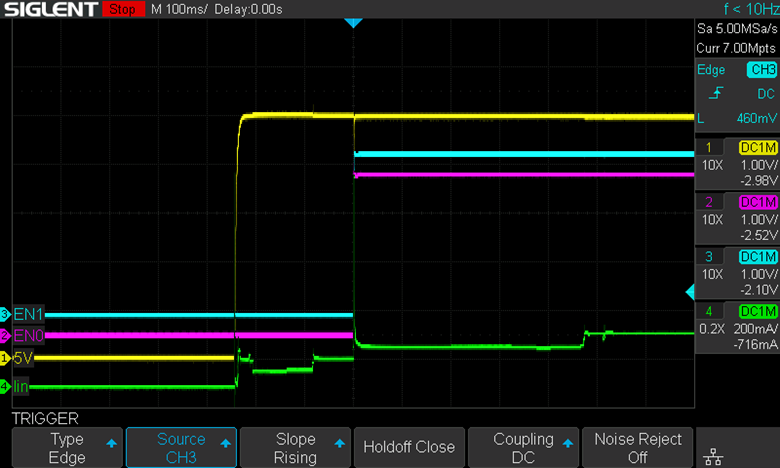
LAB: Power Analysis ------ ( ✓ )
====== REV 02 ======
Errata Items Address ------ ( In Progress )
Schematic Update --------- ( In Progress )
PCB Update ------------------ ( )
Design Review -------------- ( )
Order + Assemble --------- ( )
LAB: Sparkup ---------------- ( )
Documentation ------------- ( )


 Carbon
 Ben Holmes
 Nick Sayer