-
LAN95xx EEPROM Programming
02/04/2025 at 05:35 • 0 commentsThis is a bit of a follow-up from one of my previous logs (Auto-Negotiation Issues). At the end of that log, I came to the conclusion that I could resolve the issue by disabling auto-negotiation in windows device manager. This was just a temporary solution. For the long term, I wanted to investigate using the EEPROM to store the default configuration of the PHY.
So long as you are using a supported EEPROM, then the process of programming it is very pain free. You can use either the “LAN95xxUtility-v3_2_0_0 GUI” or “9500eeepApp_V2.5” both of which can be found here on Microchips website. As you might expect the GUI application provides… a GUI… whereas the second file provides an executable that can be called from the command line. In my mind the GUI application (LAN95xxUtility-v3_2_0_0 GUI) is useful for quick test work, whereas the executable (9500eeepApp_V2.5) would be invaluable for manufacturing in volume.
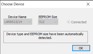
Let’s first look at the GUI… When you first launch the app you’ll be greeted with a device connection window. In my case it recognized the device as LAN9513/14 and the EEPROM size as 512KB.
![]()
The LAN95xx Utility then launches, with the below window. Checkout the readme on microchips website if you want to read into the details… but it’s a pretty nifty tool! For my project I’m modifying the manufacturer, product and configuration strings, but most other settings are left at their defaults.
![]()
Without thinking I bumped all the power requirements for my device to 500mA. I also changed the power type from self-power to bus power. I thought this would give my USB device the max power that the host USB port could provide… Instead I locked myself out and effectively bricked my device. -_-
![]()
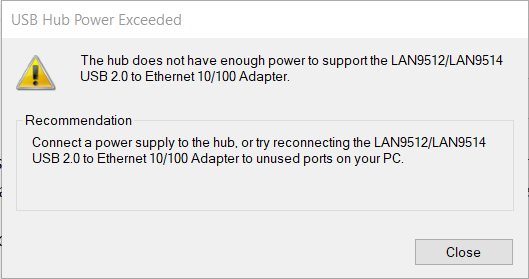
My device is bricked (more locked really) because I wrote an invalid configuration to the EEPROM. I wrote a power requirement so large that no port dare enable it. As a result, every port I tried in my lab, whether bus powered or self-powered refused to connect to the device. I can’t just write a new binary to the EEPROM because I rely on the LAN95xx controller to do the programming. Since windows won’t connect to the device, I can’t reprogram the EEPROM, and because I can’t reprogram the EEPROM, windows won’t connect to my device (it’s a chicken and the egg conundrum of my own creation). I reordered a new EEPROM and went back to the drawing board. (Maybe I could have used the command line tool to wipe the EEPROM? Future thing to try...)
Where I went wrong? Let’s do some reading…
Bus-powered hubs: “Draw all of their power for any internal functions and downstream facing ports from VBUS on the hub’s upstream facing port. Bus-powered hubs may only draw up to one unit load upon power-up and five unit loads after configuration. The configuration power is split between allocations to the hub, any non-removable functions and the external ports. External ports in a bus-powered hub can supply only one unit load per port regardless of the current draw on the other ports of that hub. The hub must be able to supply this port current when the hub is in the Active or Suspend state.” [USB Specification 2.0]
Self-powered hubs: “Power for the internal functions and downstream facing ports does not come from VBUS. However, the USB interface of the hub may draw up to one unit load from VBUS on its upstream facing port to allow the interface to function when the remainder of the hub is powered down. Hubs that obtain operating power externally (from the USB) must supply five unit loads to each port. Battery powered hubs may supply either one or five unit loads per port.” [USB Specification 2.0]
Now that I understand the standard a bit better I first flashed the NEW EEPROM and confirmed it was working. Next, I increased the current requirements to something more reasonable and tried flashing the EEPROM again… And CRAP! Not again!
![]()
At 250mA I’m locked out of thing. Once again on every USB port I have semi-bricked device, that needs its EEPROM swapped.
I have some questions… Why the heck won’t any of my USB ports support a 250mA device? Both bus-powered and self-powered hubs are supposed to be allowed to draw five-unit loads? (at least once configured). I know my device draws 250mA, and has been running on multiple USB ports happily. It seems like this conundrum is pointing toward a misinterpretation, or at the very least some bad assumptions on my part.
*TO BE CONTINUED*
-
Overcoming USB Overcurrent
02/03/2025 at 05:50 • 0 commentsI was using the device for awhile without any capacitance for the downstream ports. When I finally added 120uF to each of the 3x USB ports I was blessed with a symphony of windows device connect/disconnect notifications.
It doesn’t take much effort to theorize the issue. The second the USB load switches are enabled, and the 120uF bulk capacitors are allowed to charge, the host is hit by a tremendous di/dt demand. This could either trip overcurrent at the host, or it might just sag the local 5V rail enough that it resets the device.
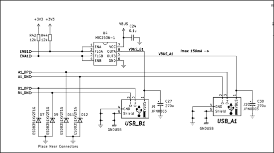
Here’s the critical sections of the circuit WRT this issue. When I first designed the circuit, I read up on the USB protocol, and noticed it called for 120uF for each port… I slapped down 270uF since that’s what I had in my parts bin. I later dropped this down to 120uF when I observed the first connection issue, but the behaviour was unchanged. (foreshadowing - spoilers I should have read the spec more carefully!)
![]()
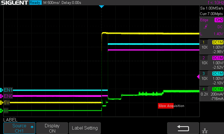
First things first, I had to do some fact finding to understanding this issue better. Here’s a waveform of the general power up sequence.
![]()
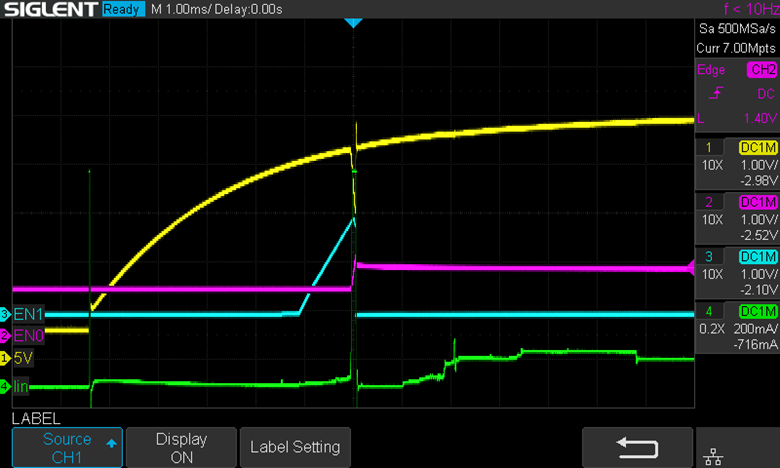
The waveform shows the enable lines (ENB1 and ENA1) from the schematic, external 5V provided by my trusty bench PSU, and the current on the 5V line. Note that when the enable lines are HI, they enable the output of U4 which provides power to the USB devices, hence charging the 120uF caps.
There seems to be two spikes on my current waveform (channel 4 – Green). One which occurs while 5V is ramping, and another that occurs ~200ms afterwords, when the enable is asserted.
Let’s check the first enable…
![]()
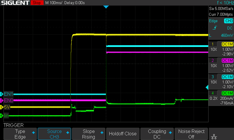
Yikes!!! There are actually two pulses that saturate my current sense amplifier (CSA) which is clipped around 850mA. One spike occurs when the device is first connected to power. This is reasonable enough since there’s some significant capacitance on the board. The second spike is more concerning since it seems to be caused by my enable pin floating high and allowing the USB ports to be powered on briefly.
Checking the datasheet for my USB load switches (MIC2536) shows we’re right in the ballpark of their enable thresholds.
![]()
I briefly probed the 120uF cap with channel 2 to confirm it was truly being enabled, and yup that cap sure is charging!
![]()
I started to toy with ideas relating to the power sequencing of the project. I could (1) delay the 3V3 startup, (2) slow down just the pull-up (PU) voltage somehow with some clever passives, or (3) just remove the damn PU’s entirely.
Idea 3 was easiest to investigate first, and seemed reasonable based on my foggy memory of the LAN95xx chip. That fog was cleared by a quick reference to the datasheet. The LAN95xx does indeed provide its own internal PU, which in theory wouldn’t be applied until it enables itself (hopfully near that 200ms mark we saw earlier).
![]()
Removing the PU resistors resolved the false trigger issue, see result below. Next up is the massive pulse from the bulk capacitors.
![]()
Hindsight is 20/20…. 120uF per HUB!
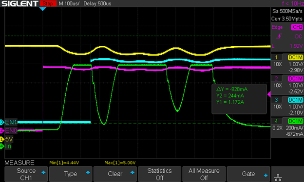
Here’s a zoomed in look at the massive gulp of energy those 4x 120uF capacitors demand. The current waveform is completely clipped. I expect the true peak current approached 2 or 3 Amps. I did some investigation into different load switches with better current limiting/soft start features, but didn’t find much that fit the bill. Then it hit me…
![]()
While designing the board several months ago, I remember thinking 120uF per port seemed ridiculously large, but I sort of shrugged it off. After working on the bug for a little too long I thought I’d better double check the standard. And yup I missed a crucial declarator… its 120uF per HUB minimum! Not per port, Doh!
![]()
Now we can safely decrease the capacitance at each port to 47uF. Decreasing the capacitance to 47uF and rebooting yielded the waveform below. It seems like 5V no longer sags to the same extent as before, but the overall current draw is still far too large (once again clipped by my amplifier).
![]()
The best solution here would probably be to swap out the load switch mic2536. This device theoretically current limits to 500mA, however we can see above it sure seems like this limit isn’t being applied fast enough. To address the lingering overcurrent issue, I decided I’d add the below circuit across the 5V rail. It will slowly charge during startup, then when the USB power is enabled D1 will turn on and help hold up the rail. Some caveats here though...
![]()
This circuit relies on impedance in the power delivery to help sag the rail. If the rail doesn't sag, this circuit will not help. It requires a very low drop Schottky diode to function properly. Sadly, the best thing I had was a 1N5817. Nevertheless I scabbed it onto my circuit to test it out.
![]()
And here’s the waveform…
![]()
Very interesting. The problem isn’t gone, but its behaviour has definitely changed. I’ll need to buy some better Schottky diodes to evaluate this solution further. I also need to assemble another current sense amplifier for this current range (no more clipped current waveforms!). See you in part 2!
Feb.8.2025 - Fixing the thingUpdate, I got some better diodes. My main concern was the forward voltage drop. For the big bulk cap to be enabled so to speak, I need the 5V rail to sag. The amount that 5V sags depends on its source impedance. The only thing I can guarantee WRT the source impedance is that it will at least have a ferrite inline. Beyond this the USB cable length and quality will mostly dictate the impedance.
Based on this I'd like to have the lowest Vfd I can find…. I was looking for something around 0.3Vfd @1A, but honestly something closer to 0.2V or 0.1V would be best (pretty unrealistic!). There were some parts that looked reasonable, but in the end I found some interesting ideal diodes that seemed promising. I've never used an integrated ideal diode, but the spec's were tantalizing enough to give it a shot (Nexperia NID5100). It seemed like a good part to have for future work, so I ordered 100… yes I have a problem.
I made a small perf board circuit w/ the new ideal diode. I probably should have done a test board of just the ideal diode but c'est la vie. It’s the same circuit I shared earlier, just with D1 replaced with the ideal diode.
![]()
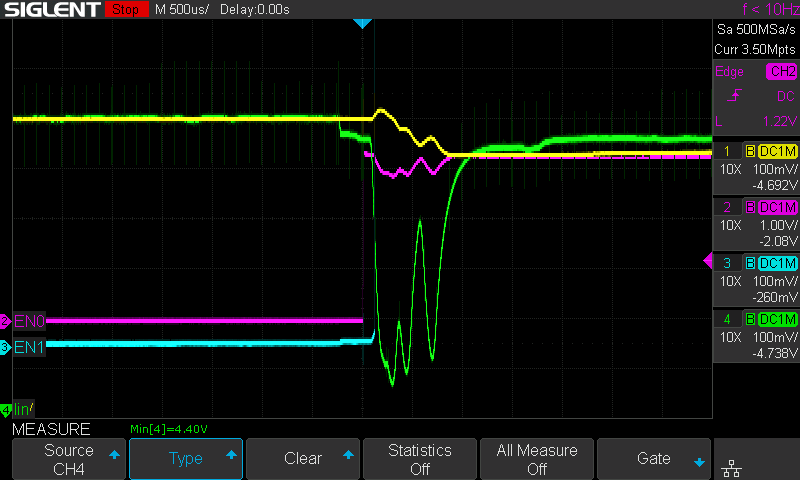
Here's the result.. CH1 (yellow) is the voltage across my bulk caps, and CH4 (green) is the voltage on the 5V rail. It seems like the bulk cap is doing its job and dumping all its stored energy onto the 5V rail during the transition. I'd really like to measure the current waveform being dumped by the bulk cap, but I'm happy enough seeing that the capacitor is discharging (yellow waveform). What's even better is this fixed my windows device connect/disconnect issue
![]()
For the next board revision I'll add this circuit, but might tweak the values a bit…. For example I'll probably increase the charge resistor to help reduce inrush current.
Solution added to REV 1.0 errata…
(1) Reduce the port capacitance to 47uF, down from 120uF (likely change to MLCC now)
(2) Add the bulk capacitor circuit
-
Auto-Negotiation Issues
12/01/2024 at 21:38 • 0 commentsSo, I have 2 of my 7 assembled boards that weren’t working as expected. I was able to quickly narrow it down to the connection between the two PHY’s (uh-oh). Immediately I was suspicious of my home-brew coupling network that replaced the magnetics we normally see.
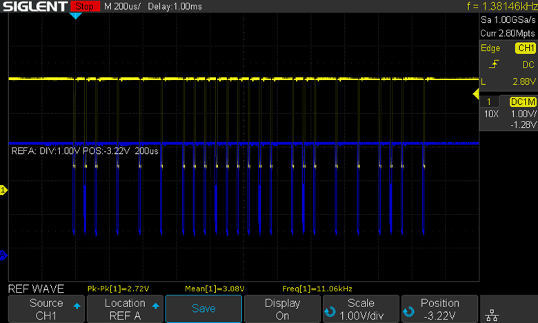
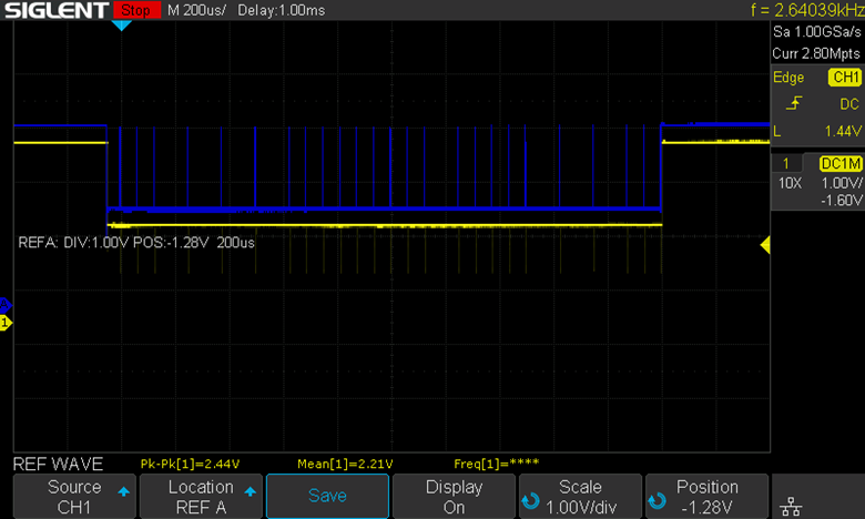
After a lot of sniffing around the circuit I wasn’t able to see anything out of the ordinary. FLPs (Fast Link Pulses) were being sent and received by both PHYs, but no link was ever established. I ended up comparing to some of my known good PCBA’s and noticed something interesting about the FLP of my problematic DUT.
Here’s what the FLP’s look like that are being received by the IC+ PHY on my problematic unit.
![]()
And here’s what those same signals look like on a working device.
![]()
Very odd. I thought this difference could be caused by a lack of Vref on IC+ (since the rail seems to sit around 3V3 when I’d expect it to be closer to 1V8), but after looking closer at the supporting passives around the IC+ PHY everything seemed in working order.
I also took some wider captures of the entire startup hoping to gain some insight, but there was nothing else unique I could find between my two DUT’s.
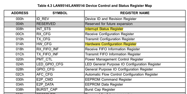
This issue led to a LARGE LARGE LARGE rabbit hole of trying to read the internal registers of the Microchip PHY (the one sending the above pulses). There are some very handy registers that would have helped me debug this issue (see below).
![]()
Sadly, I burned half a day trying to configure a system to read/write the registers of the device using blueTag and OpenOCD. BlueTag was able to recognize the device, but past that I was never able to make any significant progress in this endeavor.
To unstuck myself, I decided to disable auto-negotiations since that’s where everything seemed to be hanging (you can do this just in device manager). Doing this resolved the communication issue. If this is the fix I choose to implement it means the end user would have to muddle around in device manager before using their HUB (not ideal).
So, I have two options to investigate further. (1) Redesign the coupling network to resolve the auto-negotiation hiccups, or (2) add an EEPROM to the PHY that will store the default setting as 100base-t. Both of these options are supported by the copper on rev 1.
-
KiCad Variants with Python
11/24/2024 at 01:12 • 0 commentsMini side quest time!
So I recently watched a video from Psychogenic Technologies and learned he made a Python package that lets you easily interact with KiCad Schematics. My mind immediately jumped to PCBA variants. The same weekend, I launched VS Code and started scripting. I later learned I should have searched the web more first… There is already support for variants in KiCad and it was added this year (?) via the KiVar plugin. It looks like KiVar is very well maintained and fleshed out, so if you’re looking for variants in your KiCad project I’d highly recommend you go there.
Alas it was too late; I already created my own python module to create BOM variants. I made my github repo public, but unless you have good reason probably just use KiVar 😉
Anyways here’s my hacky way to get BOM variants into my project!
-
Enclosure Updates
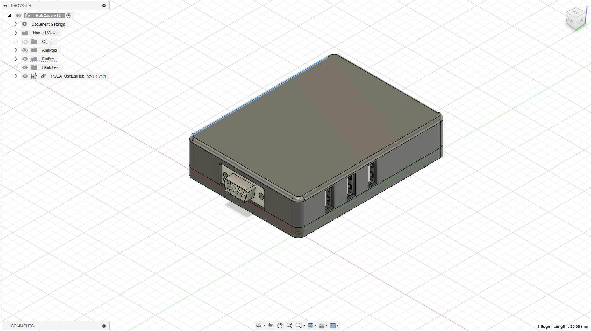
11/11/2024 at 20:58 • 0 commentsI've been working on an enclosure in the background using fusion 360. I have a couple tweaks to make to the enclosure, but for now this is what it looks like. STL files have been added to the project files. For future updates to the enclosure I'll edit this log.
![]()
![]()
-
Blender Render - Side Quest
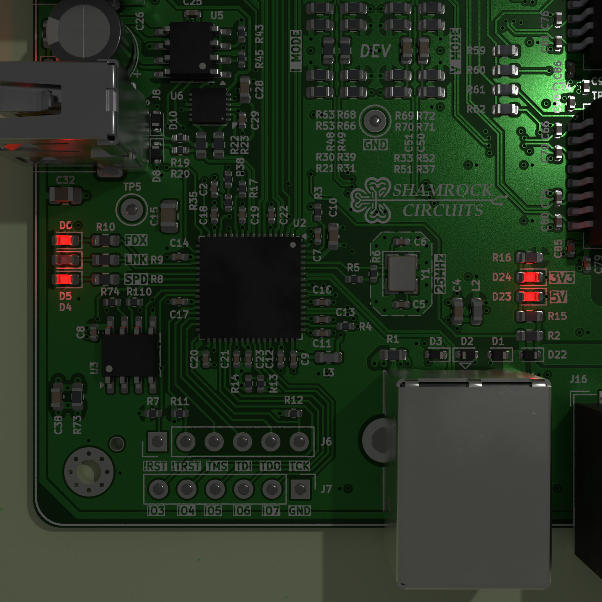
11/07/2024 at 16:46 • 0 commentsI opened up blender for the first time in two years to test out the pcb2blender plugin for Kicad (here). Shown below was my first attempt. I'm pretty happy with the results, but there's still lots of tweaking/learning ahead [those LEDs for example]. I'll update this log later when I have some more time to play with the tool.
![]()
Update - The next morning I was able to create this one. I'd really like to learn how to generate a realistic glow on the LEDs, but I think that will have to be a full weekend project. Coming from other CAD tools like fusion and KiCad, Blender has a very unintuitive user interface (I did the donut tutorial, but that was >2 years ago now).
![]()
Second Update - I spent Saturday learning how to create a short animation, and how to create a more realistic lighting affect on my LEDs. For the LED’s I ended up separating the mesh using the “bisect” feature, and assigned a different material to the transparent portion of the LED. Then I placed a small point light source inside the transparent material. I did similar for the RJ45 connectors.
![]()
To make the light blink I followed this handy tutorial (How to Make A Flickering Light in Blender), and for tips on the animation workflow I followed Blender Guru’s legendary donut tutorial (Part 12).
Here’s the end result....
In the future, I’d like to do another animation including the enclosure, and have the components dropped onto the PCBA. For now though, I’ll call my Blender side quest a success.
-
Documentation Update
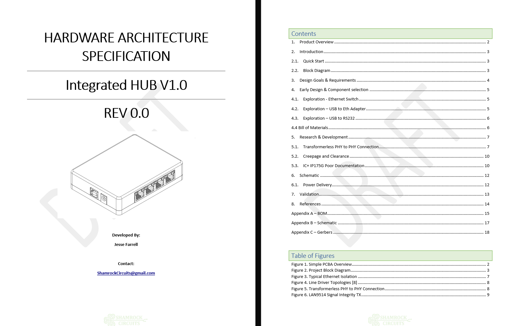
11/04/2024 at 15:59 • 0 commentsI did a big documentation push over the weekend and added 3000 words to my hardware architecture spec document. If your interested in the details of this project, or are looking to do something similar I recommend you take a look in this projects attached documents.
![]()
Note, its still technically unreleased since I need to add sections for creepage and clearance, validation and likely some other sections which don't exist yet.
-
Rev1.0 Release
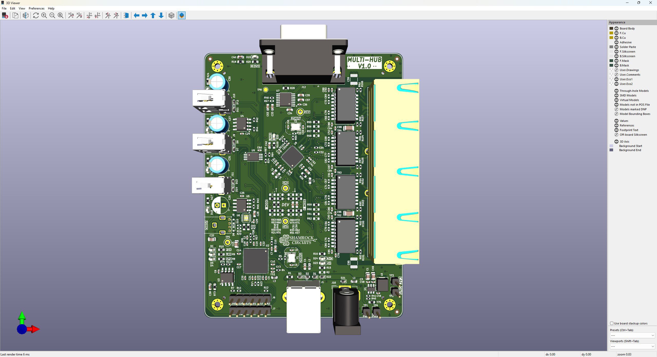
10/20/2024 at 15:22 • 0 commentsQuick update: The next revision of the board has now been ordered through JLCPCB. I’m using pick-and-place for about 95% of the board. The remaining parts are straightforward to solder or a one-off part. I couldn’t justify paying the reeling fee for the extended part.
REV1.0 – Layout
![]()
REV1.0 – 3D Model
![]()
![]()
-
Creepage & Clearance - Attempting Standards
10/09/2024 at 05:15 • 0 commentsWhile I don’t know if I’m truly a green engineer anymore, I’m definitely a little wet behind the ears when it comes to standards. I thought it might be a good exercise to determine the creepage and clearance requirement for isolation on my ethernet circuit. The result was/is a large can of worms.
What are the requirements?
I’ve seen the requirement waved around on several occasions… ethernet transformers are designed to survive 1500Vac, and sure enough looking at 802.3 (IEEE standards that outline ethernet) you can find this spec listed in various locations throughout the PDF. Interestingly its only ONE of 3 possible isolation tests. from 802.3; “this electrical isolation shall withstand at least one of the following strength tests”. The other options include being exposed to 2250Vdc or a short impulse.
Bare minimum – Withstand 1500Vac @60
Approach Number 0
The zeroth approach might be just to look at the IPC-2221B(?) design standard for C&C (creepage and clearance) recommendations. I didn’t go down this route. Though this standard can be invaluable, I don’t believe any safety standard would point us in its direction.
Approach Number 1 - Start from the directives
My first thought was to start from the directive and work down to the product standard, if one exists. I’m a little more familiar with the EU framework, so I’ll start there by looking at Harmonized Standards listed by the European Commission.
Scrolling down the list there are several directives that would be of interest. General Product Safety (GPSD), Low Voltage (LVD), and Electromagnetic compatibility (EMCD). I’m adding the “D” here in the acronym since I’m referring to the directive (though I think GPSD is now a regulation?).
NOTE. If you click on the directive and scroll down to the bottom of the webpage you can look at a “summary list as pdf document”, this is how I found the list of harmonized standards for each directive.
Not having too much experience with standards my C&C spec could be hiding under any one of GPSD, LVD, or EMCD. I quickly learned my product doesn’t fall under the LVD since that directive covers “electrical equipment operating with an input or output voltage between 50-100Vac or 75-1500Vdc”. From the GPSD, it seems like I need to consider EN IEC 62368-1:2020, this standard concerns “Audio/video, information and communication technology equipment – Part 1 : Safety requirements”. My project is essentially a big communication adapter, so I believe it would comfortably fit here. From EMCD I’ll be looking into EN 61000-6-1:2007, EN 61000-6-3:2007, EN 55032:2015, and EN 55035:2017. These standards relate to immunity/emission “for residential, commercial and light-industrial environments” and “Electromagnetic compatibility of multimedia equipment”.
Already I’m not a happy camper, this is a lot of overhead to get one value…
After looking at each standard, it seems like 62368-1 has the info I need. Table 14 provides the “minimum clearances using required withstand voltage”. If I assume the definition of withstand voltage is the same between IEEE 802.3 and IEC, then I should be able to read the clearance right off the table. The lingering question is, does my application require reinforced insulation? Very likely it doesn’t, but I want to know how to find out.
I read the entirety of the standard the next day and I wasn’t able to gain much clarity over my initial understanding. So much of the C&C is depended on a mains connection, which I do not have for my product. I’ll do some more reading but the expected C&C value is 1.5mm.
Expected Clearance Requirement 1.5mm
Approach Number 2 - When in doubt, phone a friend
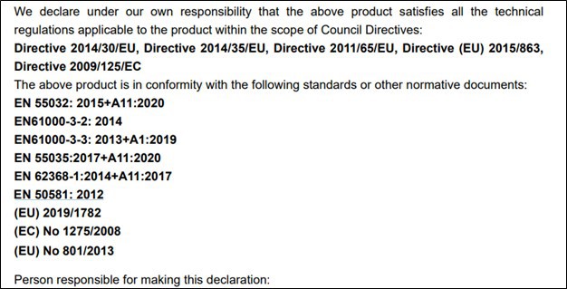
Every product with a CE mark needs to have a declaration of conformity (DoC) that outlines which standards the product complies to. If we can find a similar product’s DoC, we can get some good nuggets about the standards we should be looking at.
A quick google search for “ethernet switch with USB port” and I was able to find a nifty device that provides USB over ethernet. As far as I’m concerned, this product would fall under the same product category as my widget. The DIGI AW02-G300 has a certification tab and if you dig around the EU relevant documents, we can find the DoC for that product.
Our “phone a friend” approach quickly gave us some good standards to look at. Checking with my results in approach 1, it looks like friend’s homework is very similar to my own. Beware, I’d strongly discourage copying his homework. Best to come to your own conclusion, and use your friend as a quick gut check.
![]()
Note that 2x of my standards seem to be missing from their DoC (EN 61000-6-1(3)). If I want some more reassurance, I can always phone another friend… my next friend includes these two missing standards but also adds some extra ones (seemingly to support some directives I hadn’t identified).
![]()
Using approach 2, I was able to get some reassurance that I’m in the right place. EN 62368-1 is where I should be looking for C&C requirements.
Approach Number 3 – Start from the ethernet standards
For my last approach I will be starting from the IEEE 802.3 and then I’ll work backwards to see what standards it prescribes (if any). This approach was recommended to me by a colleague (and seems like a great idea, maybe where I should have started).
*TO BE UPDATED*
-
REV00 -> REV01 Fixes
10/08/2024 at 04:14 • 0 commentsI’ve returned from travel and started working on cleanup for 1 of 4 of my projects… this one I’m most excited about so it’s the chosen one.
Based on my spark up I had a number of errata items to address. More than I’d care to admit; but in my defense this was somewhat by design, since I knowingly pushed the board to fab without running a number of my final checks. Everyone knows that the last 5% of the project is where all the work hides… sometimes its easier to debug in HW than to pour over datasheets for minor oversights.
1) IC+ I1P75Gx – Termination Resistors
We don’t need them parrallel/shunt termination for this PHY. It even says on the front page of the datasheet (BUT LITERALLY NOWHERE ELSE!!!) “built-in 50 ohm resistors for simplifying BOM”. Removing the 50ohm parallel termination resolved the comms issue I was having.
2) USB Ports – Increase Capacitance
I hadn’t read the spec before I did my design (a horrible sin). As a result, the capacitance on my USB ports are woefully out of spec. From the USB standard “downstream facing port Vbus power lines must be bypassed with no less than 120uF capacitance”. So, I’ll add 150uF electrolytics to each port.
3) USB Port Pinout – Footprint Error
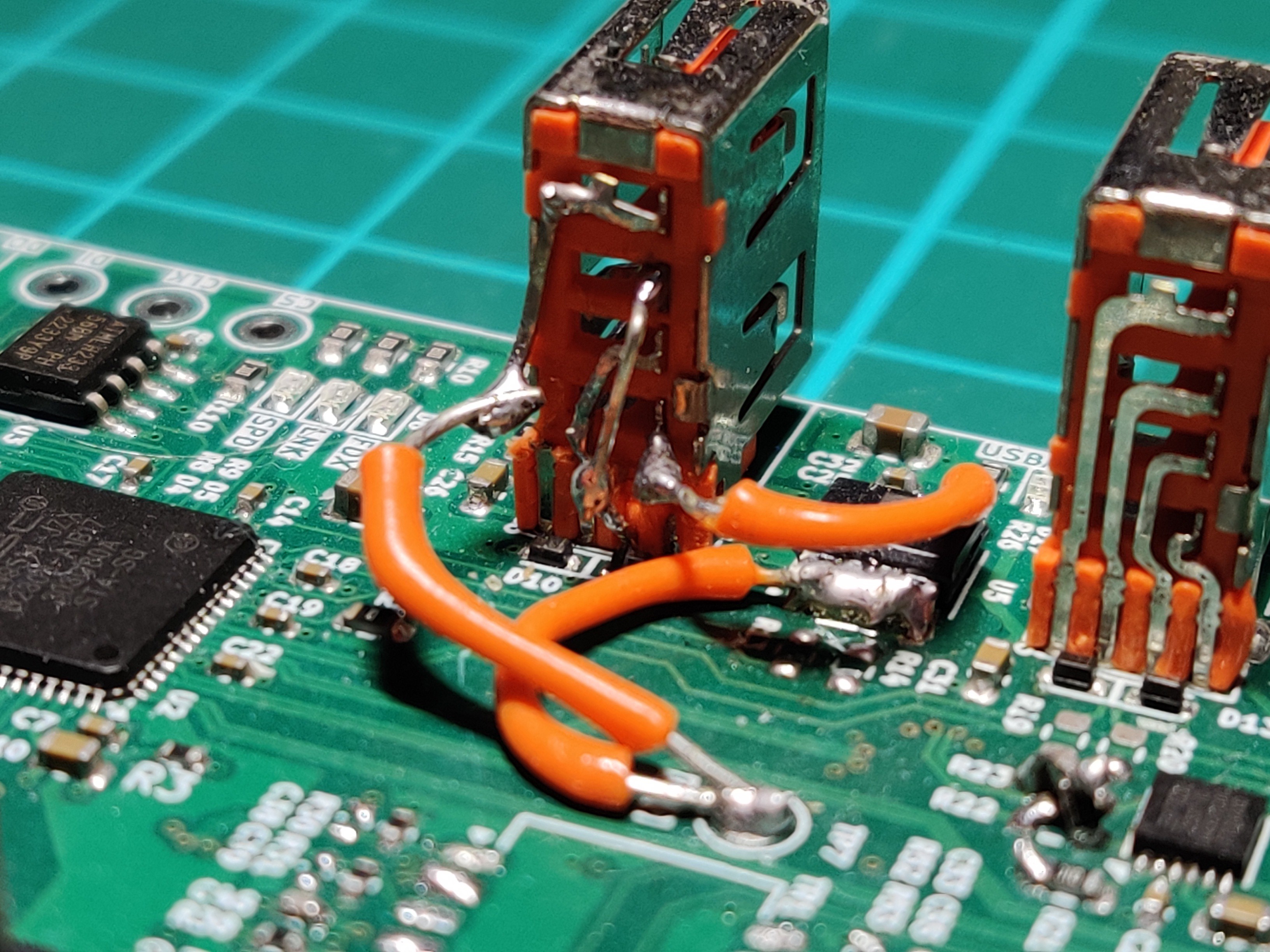
I made a custom footprint for an interesting side mount USB connector… I should have triple checked the part. The ports are completely flipped. Instead of VBUS/D+/D-/GND, my footprint had GND/D-/D+/VBUS. To test the circuit for spark up I had to make a disgusting bodge. But it worked!
![]()
4) FTDI – Pinout Error
Another dumb mistake. I had my D+/D- flipped going into my RS232 converter. Nothing a bodge can’t fix though.
![]()
5) Clock Stability – Bug
My first board worked fine, but the second seemed to only briefly bootup, then power off after a few seconds. I was able to narrow it down to the clock on the USB to ETH adapter. I had to add a 1M feedback between XI/XO to ensure the clock remained stable (or would it be instable…). I already had the footprint there it was just DNP’d. Easy fix, no bodge this time.
6) Power Switch Variant
To toggle the power to each USB port I’m using a pair of N channel power switches (MIC2536). These were jellybean parts recommended by a reference design so I didn’t give them much thought. This lack of thought led me to buy the first variant I saw MIC2536-2… the enable is inverted on this version, what I needed was MIC2536-1. To continue spark up I just tied the enable to the appropriate rail.
Integrated HUB - Ethernet, USB, RS232
Ethernet Switch, USB HUB, USB-Ethernet and USB-RS232 Adapter
 Jesse Farrell