 Yann Guidon / YGDES
I have revisited 16. Run Length Limitation, reduced.
This circuit has some interesting properties inside large CMOS lanes.
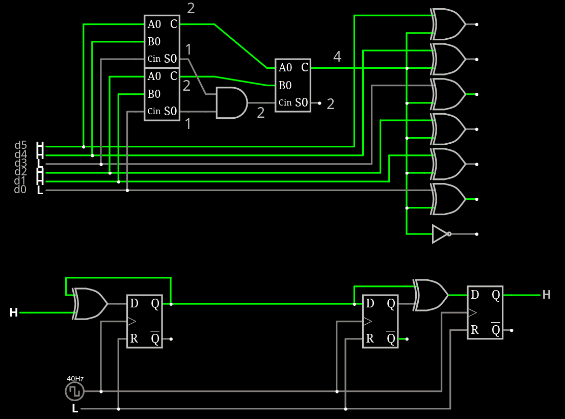
It takes 6 bits, takes the popcount and if > 3 (take the MSB) then inverts the data => no more than 3 data bits are ON at the same time.
Then a binary integrator takes these 6 bits, and at most 3 of them will be toggled in a give cycle.
Two extra signals are required and they will toggle :
- The Flip flag may change during every cycle
- The clock signal transitions 2× per cycle but a "DDR" method can be used (sampling at both edges). Even better : a 4-phase clock signal, which makes it possible to sneak control signals in.
The gPEAC's 18-bit word could be cut into 3 6-bit "nibbles" and transmitted in 3 cycles with a guaranteed number of transitions, so the energy budget can be tighter, or the margin could be increased.
The Transmission Minimisation makes it suitable for CMOS since power is drawn during each transition. During every cycle, the flip bit, the clock signal and at most 3 data bits will change, instead of 6+1=7 without the circuit. There would be a better gain with a larger bus. There is also an implied parity which catches some blatant errors.
This system would be great for CPU-RAM interchip communication too.
Too bad I can't apply this to the serial link, at least directly and with tri-level signalling. TMDS works well for serial binary levels (see 33. TMDS), and also potentially for parallel 4-level signals: pairs of bits are directly encoded and the overall bus has less amplitude, so uses less power and less creates EMI.
Discussions
Become a Hackaday.io Member
Create an account to leave a comment. Already have an account? Log In.