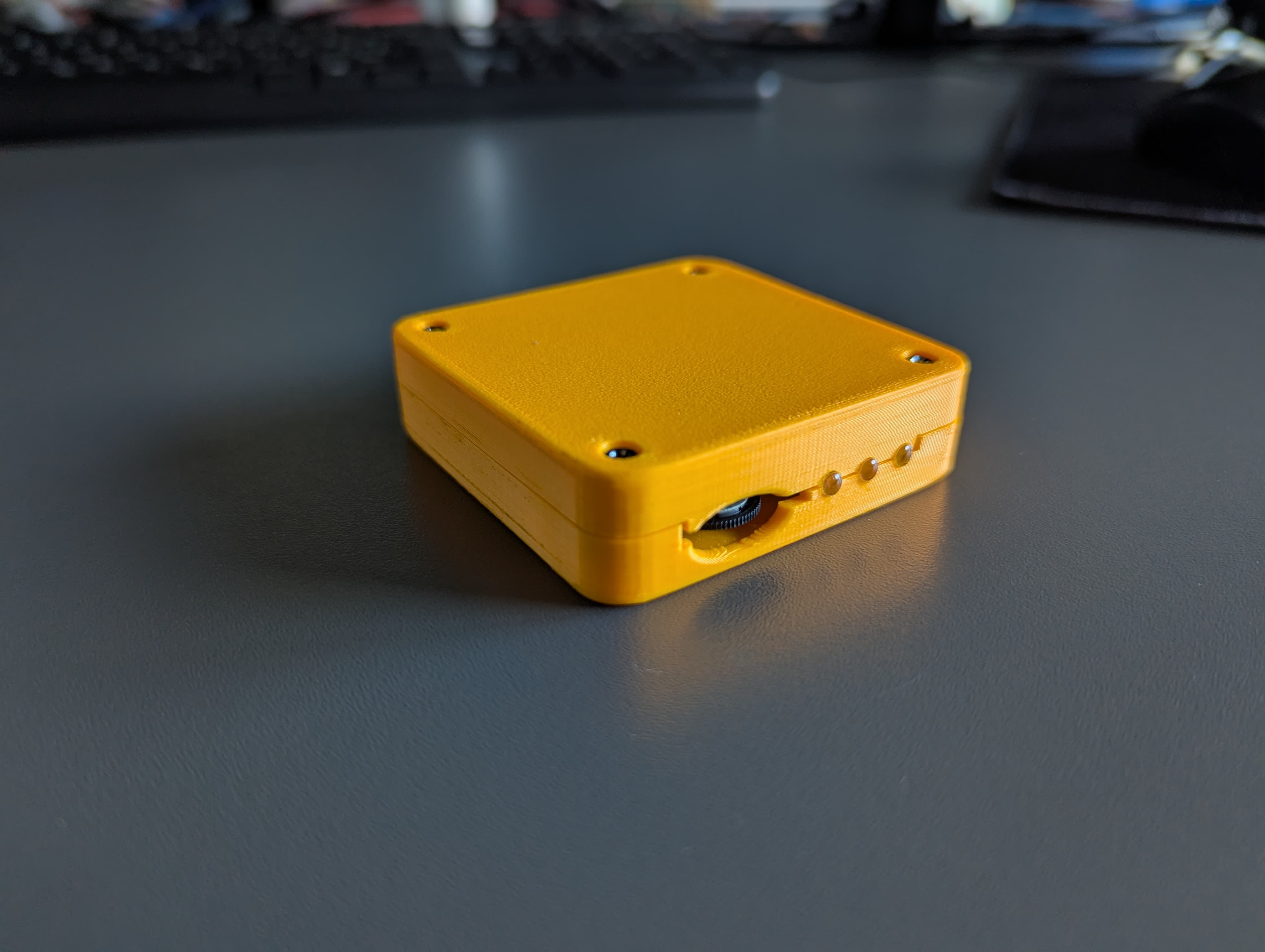
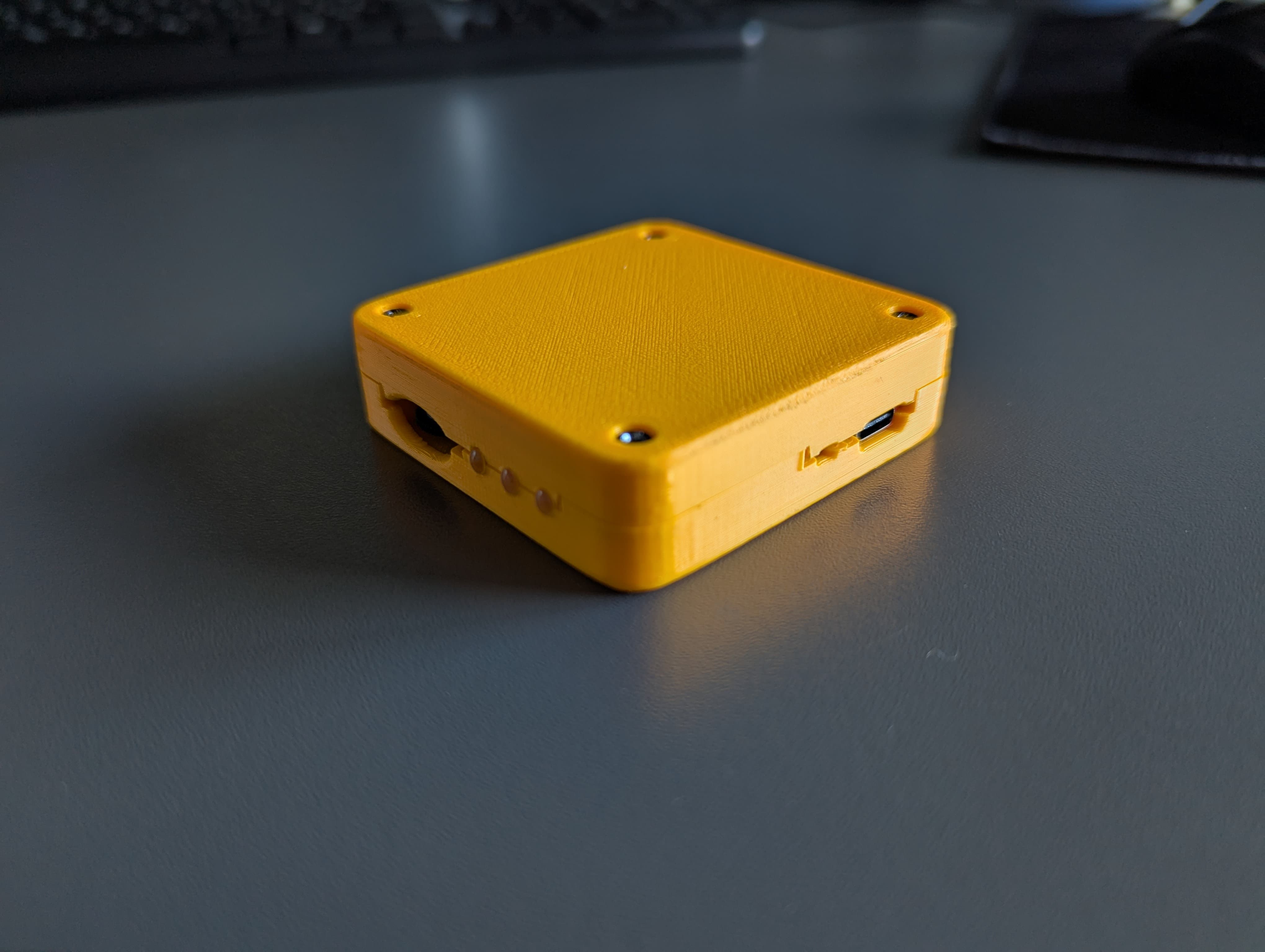
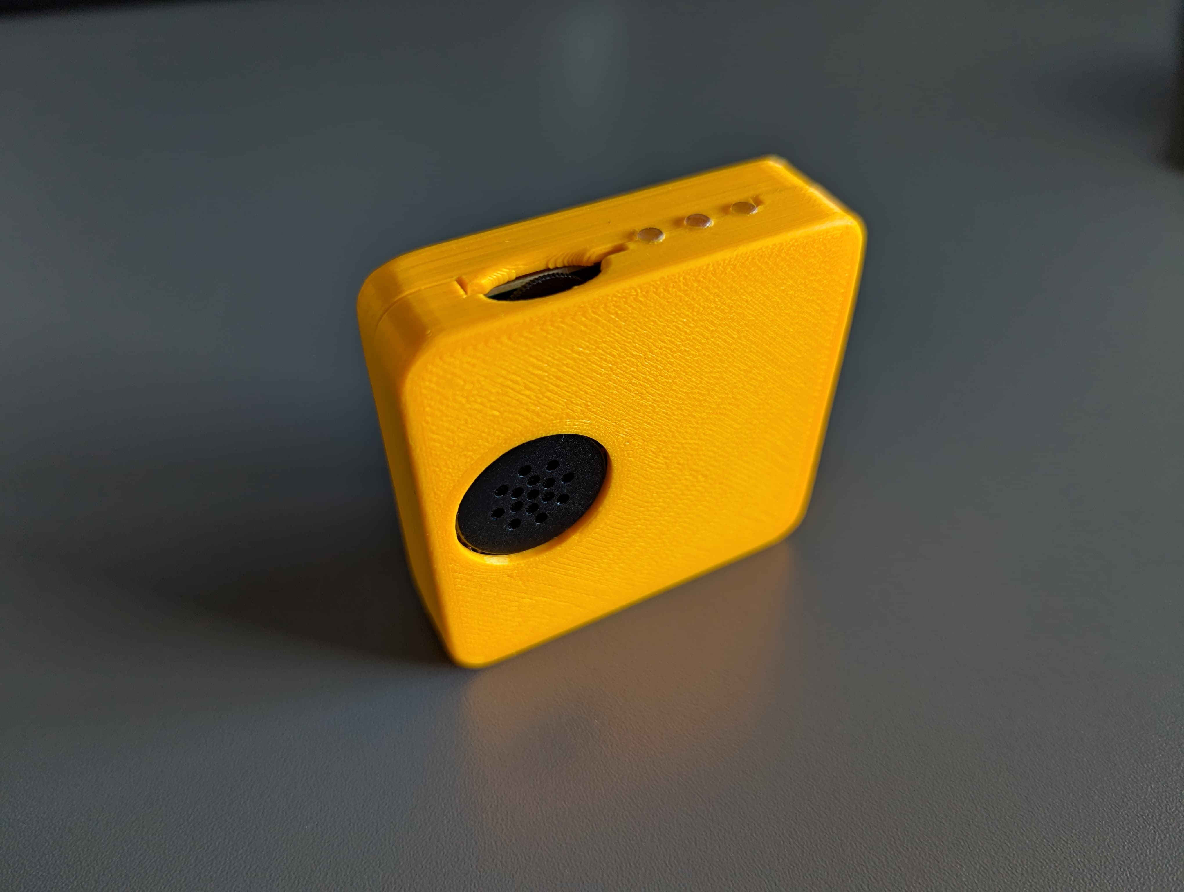
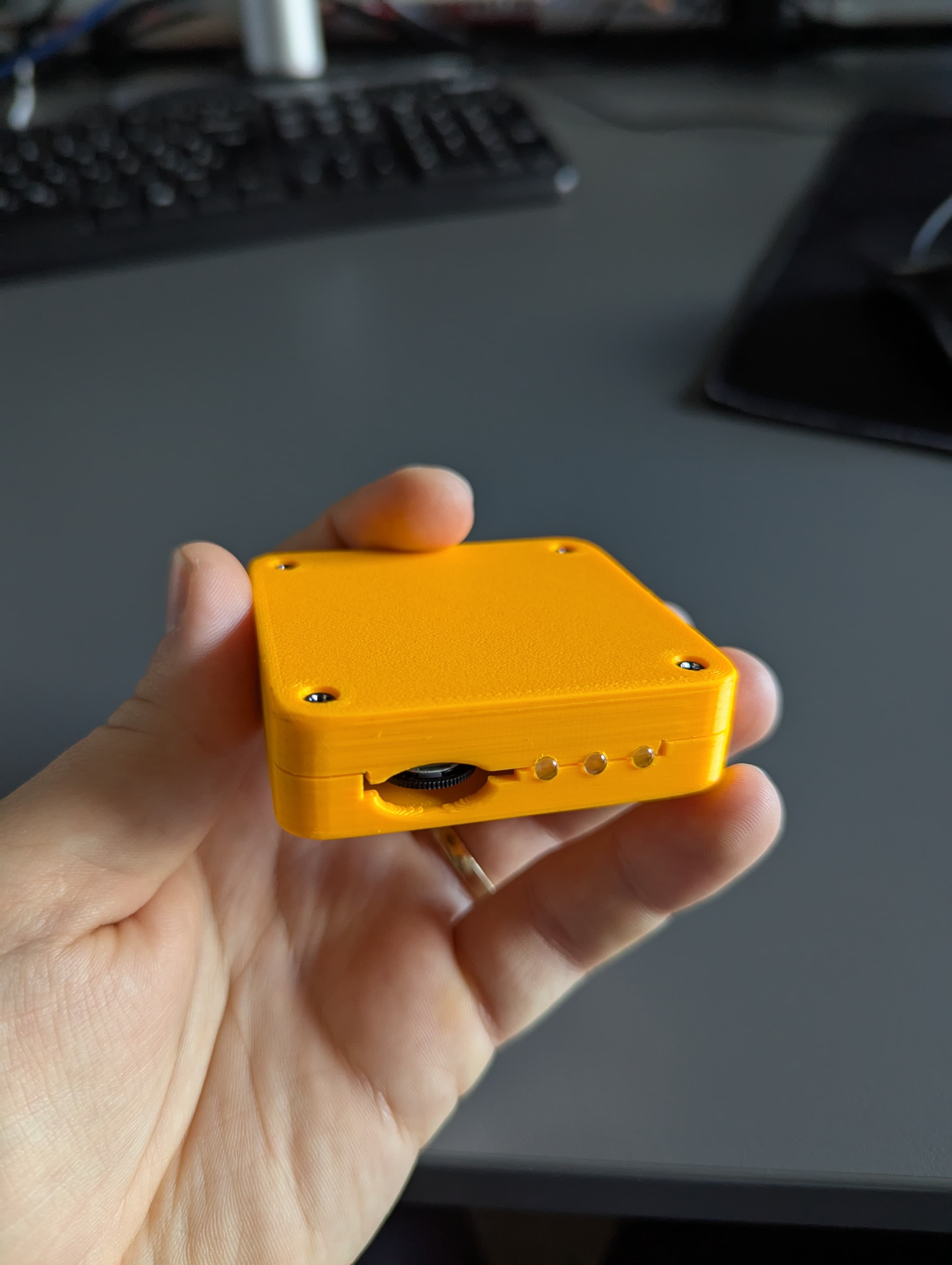
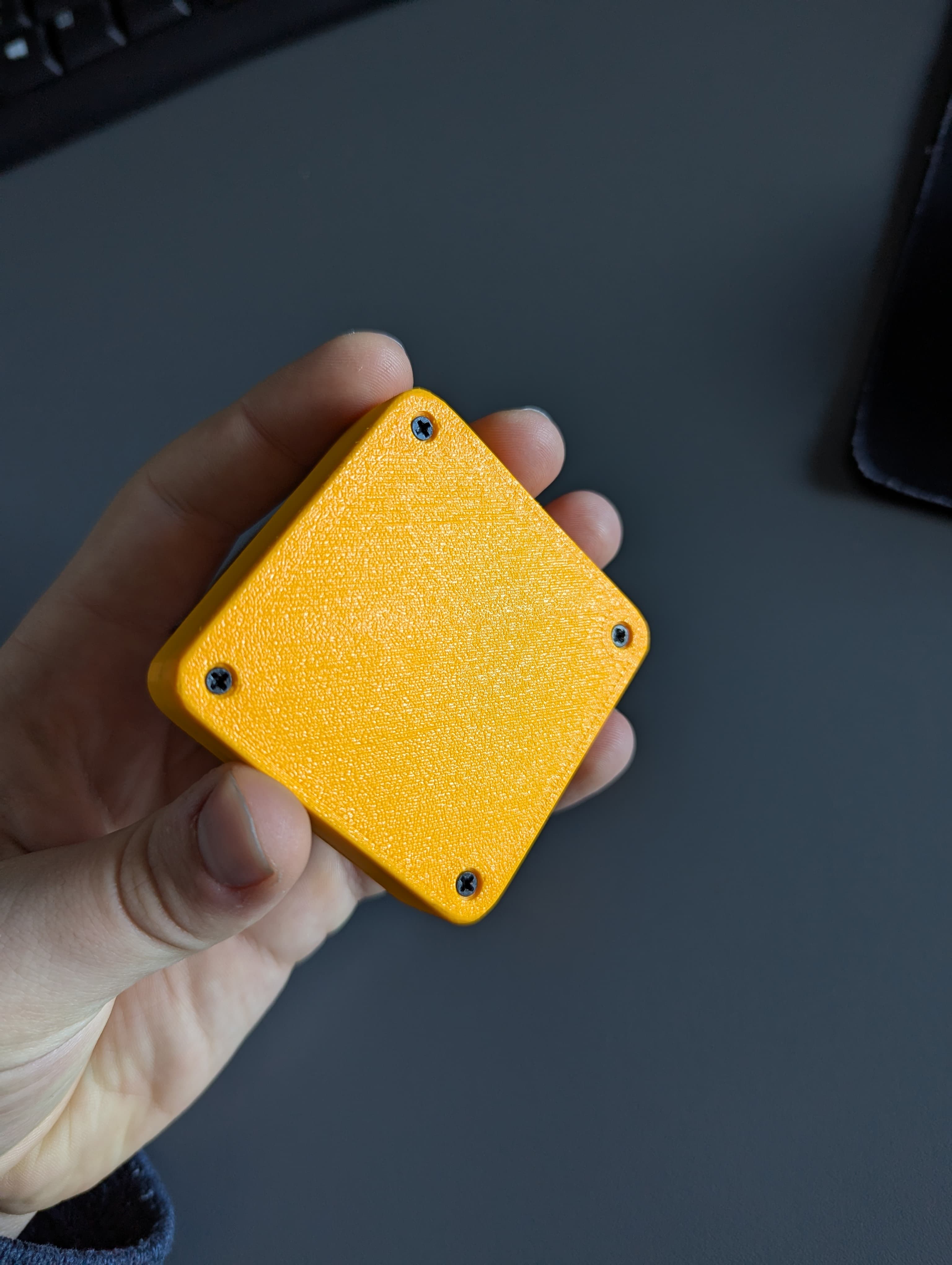
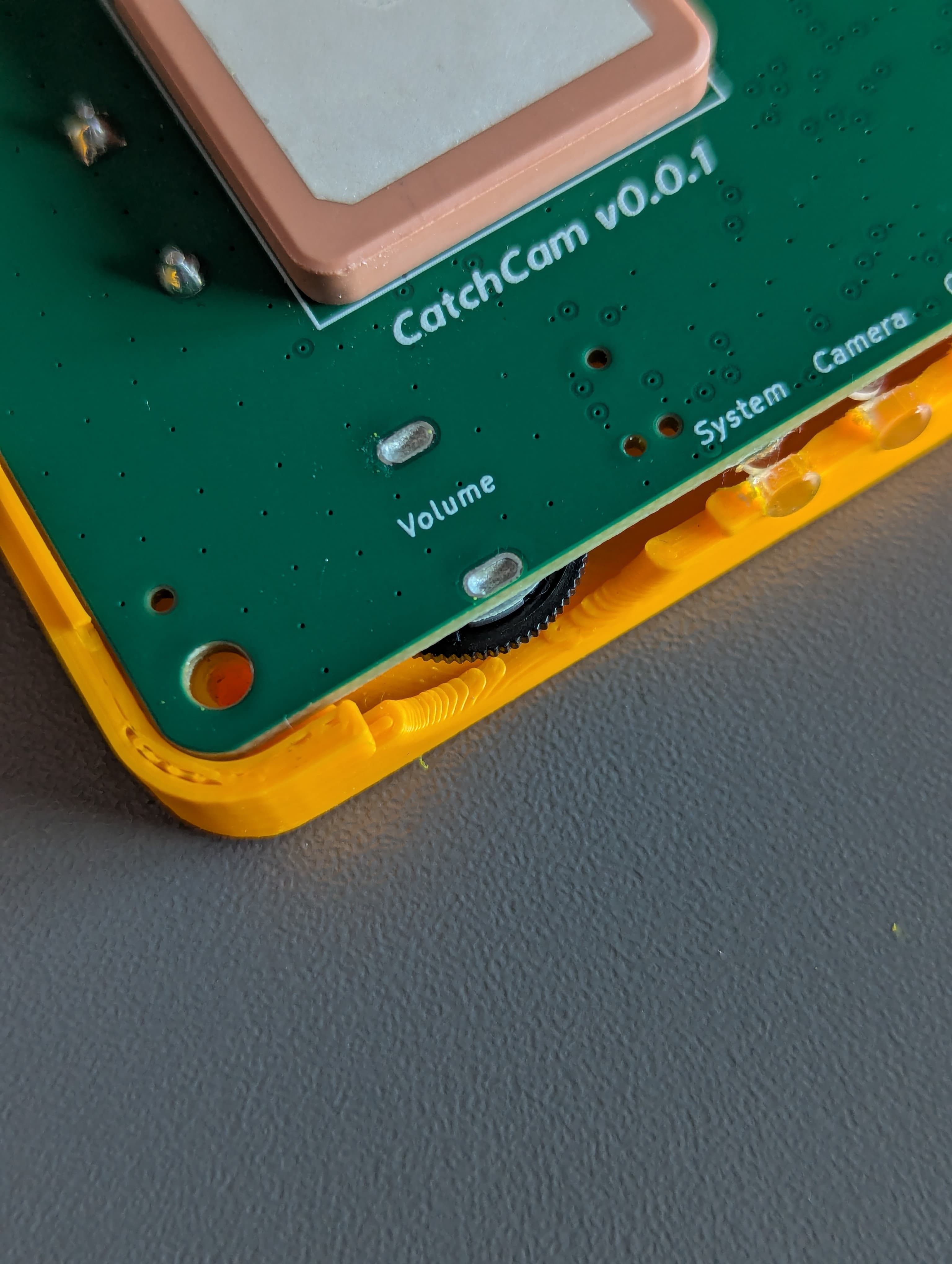
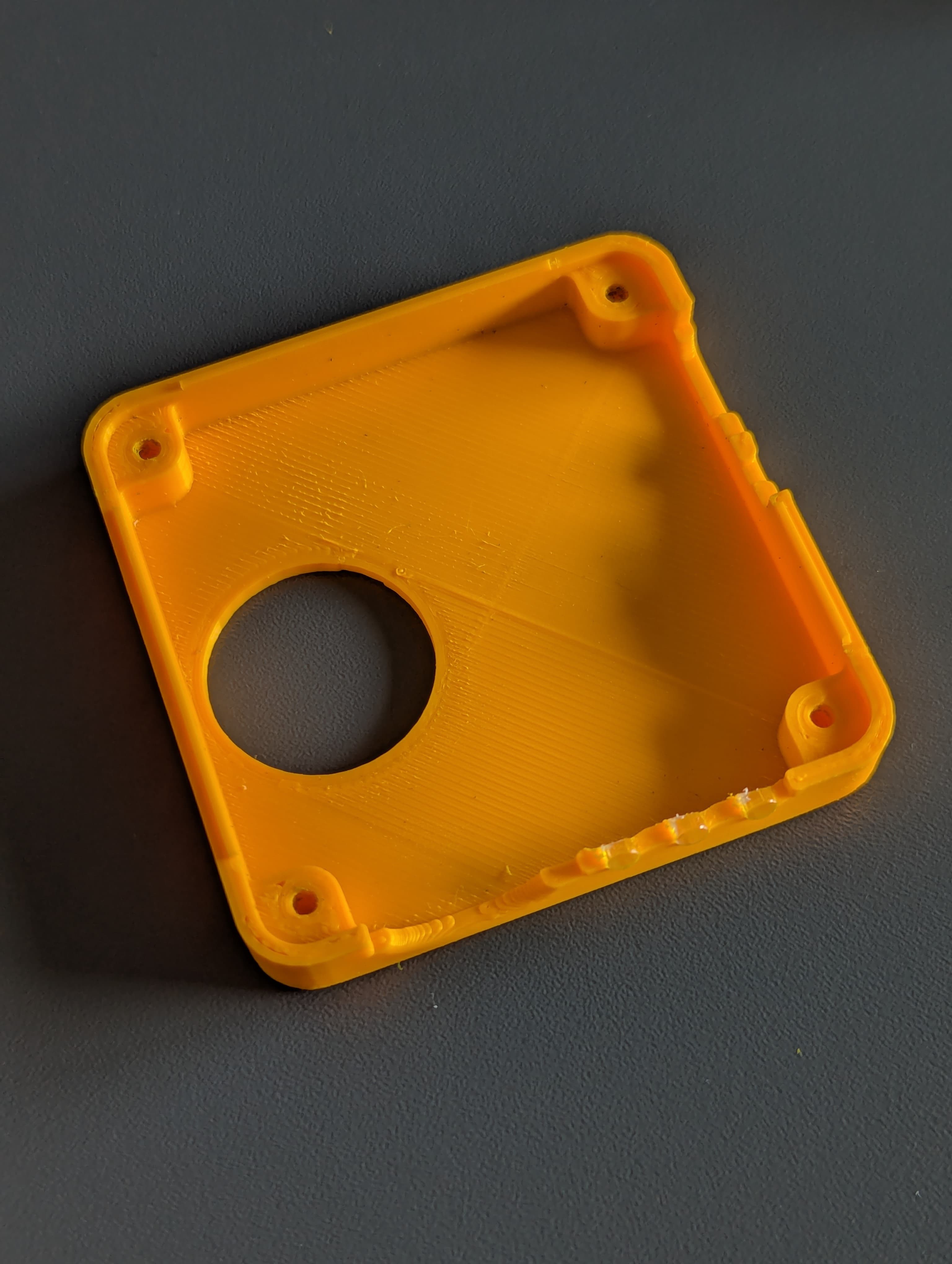
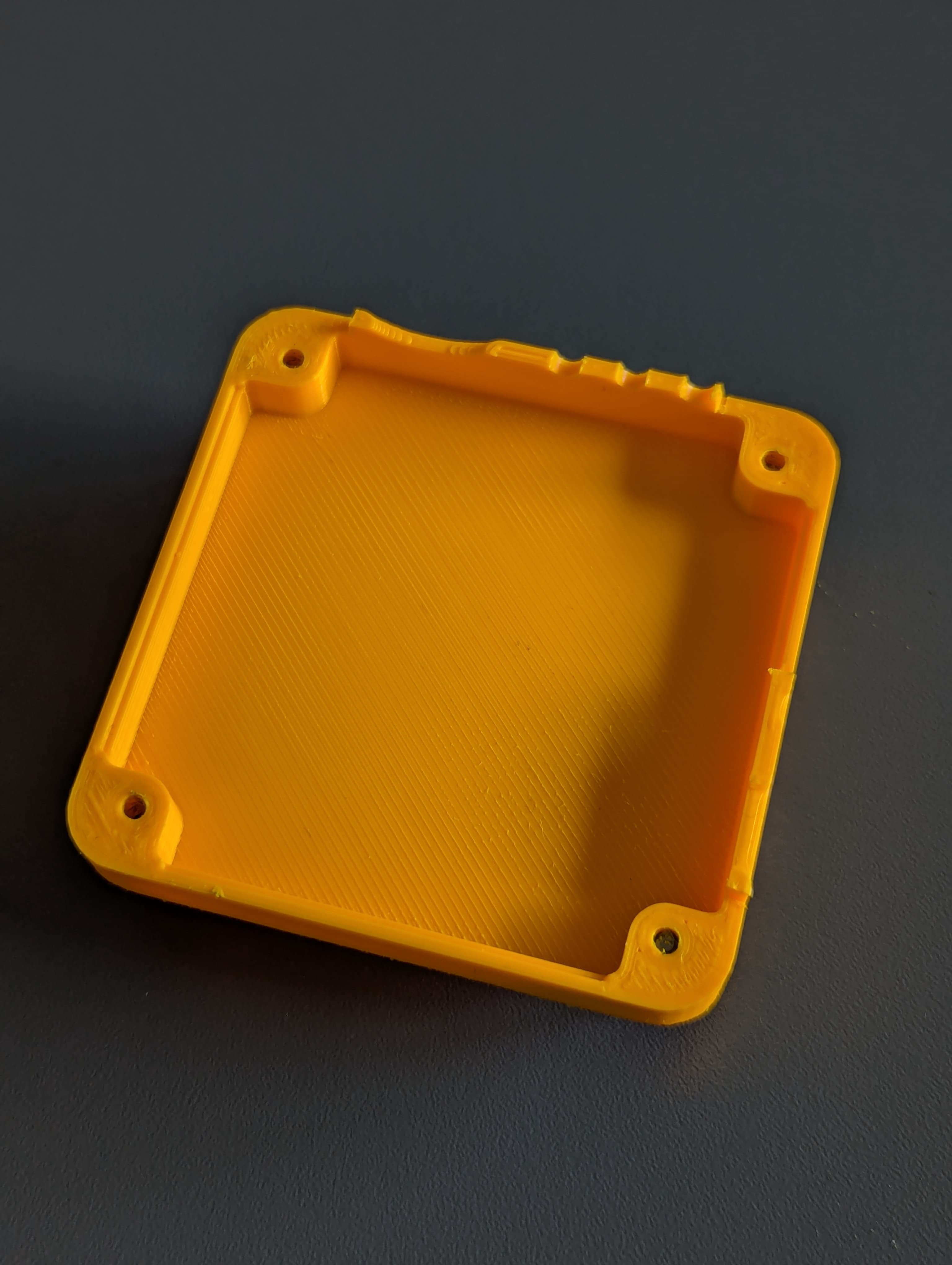
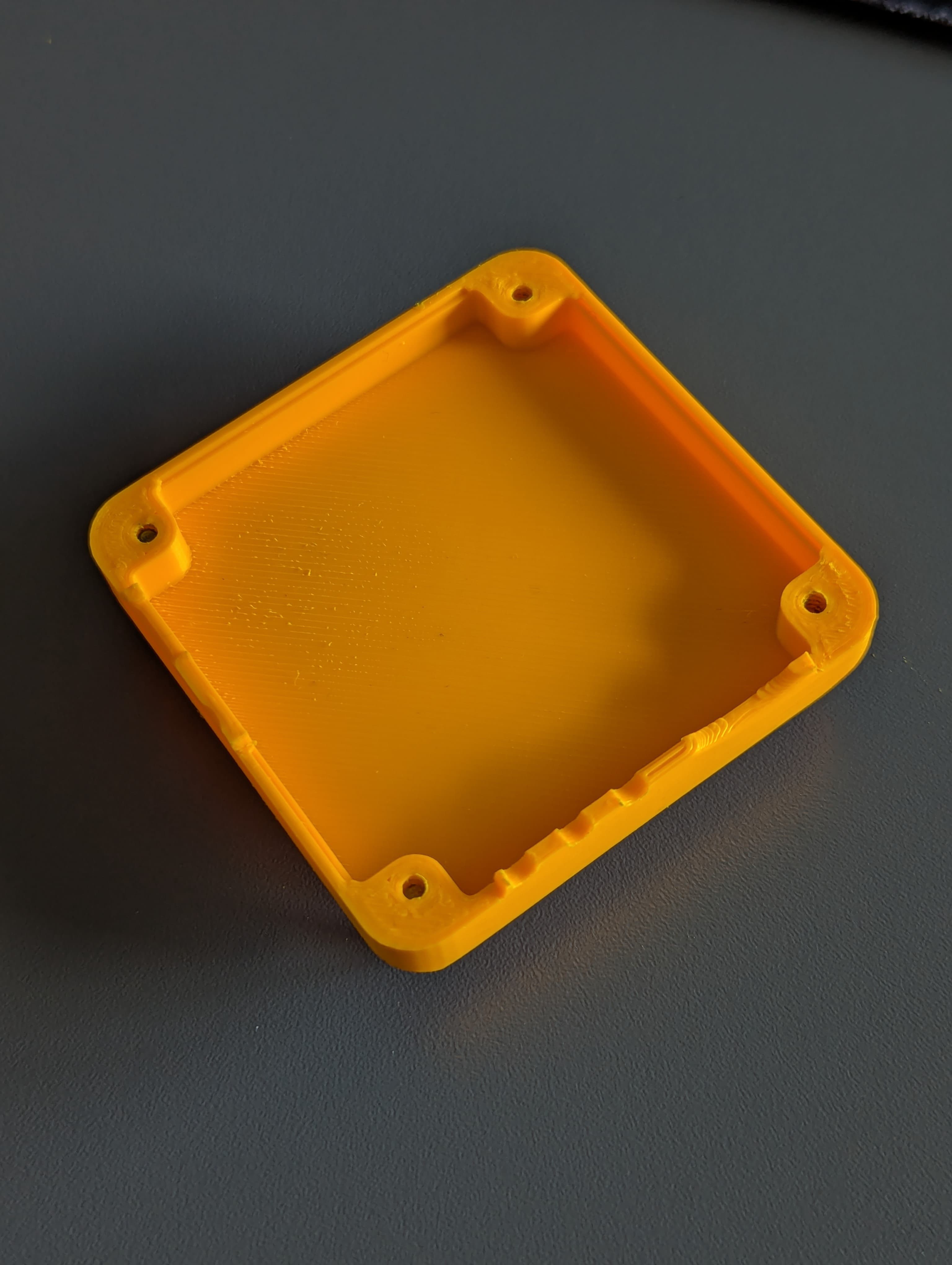
-
My Catchcam Project is Now Open Source
01/24/2025 at 15:10 • 0 commentsI'm thrilled to announce that I've open-sourced the software for the Catchcam Speed Camera Detector. You can now find it on GitHub at https://github.com/IvanVnucec/catchcam.
Why Open Source?
I decided to open source this project because I believe in fostering a open source community. By making this software freely available, I aim to:
- Encourage Improvements: I hope that developers from around the world will contribute to enhancing the functionality of Catchcam.
- Spread Awareness: More people can now benefit from knowing where speed cameras are located, potentially leading to safer driving habits and fewer violations.
Contributing
I welcome anyone interested to contribute to this project. Whether you're a developer looking to add new features, or someone with ideas on how we can make Catchcam even more user-friendly, your contributions are invaluable. Here's how you can get involved:
- Fork the Repository on GitHub.
- Submit Pull Requests with your improvements or fixes.
- Open Issues for bugs or feature requests.
- Spread the Word: Let others know about this open-source initiative and its potential to improve road safety.
Thank you for your interest and support!
If you're interested, you can pre-order a sample by sending an email to vnucec.ivan@gmail.com.
-
Enclosure Design and 3D Printing
12/05/2024 at 14:20 • 0 commentsIntroduction
After an extensive search for a suitable off-the-shelf enclosure, I decided to design and 3D print a custom enclosure for my Catchcam project. My requirements were specific: a small and easy-to-assemble enclosure. I wanted to avoid the hassle of modifying a generic enclosure by drilling holes and cutting openings. By designing my own enclosure, I could ensure a perfect fit for my project’s needs.
Note: If you’re interested, you can pre-order a sample at vnucec.ivan@gmail.com.
Design Inspiration
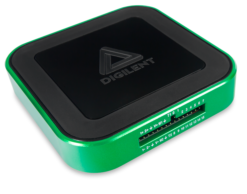
The main inspiration for the enclosure design came from the Digilent Analog Discovery 3 device. I really liked the look and feel of that enclosure, especially the rounded edges and the overall simplicity of the design. I’ve decided to go with a similar design for my Catchcam project.
![]()
Digilent Analog Discovery 3. Courtesy of digilent.com. Design Process
The enclosure is designed in FreeCAD which is a free and open-source parametric 3D CAD software. It took me a while to get used to the software, but I’m quite happy with the results. Although I have some experience with CATIA, I’ve decided to go with FreeCAD because it’s free and open-source. The journey was quite challenging because FreeCAD has a few quirks and you need to get used to the way it works. Also, FreeCAD was crashing quite often without any warning, so I had to save my work every time I’ve made some significant changes. Actually, the main frustration was that they had published a first major release v1.0 which implies that the software is stable, but it’s far from it. I’ve also tried OpenSCAD which is a script-based 3D CAD software because I love the idea that you can create 3D models using code, however, for complex shapes like the enclosure, the OpenSCAD code would be too complex to manage.
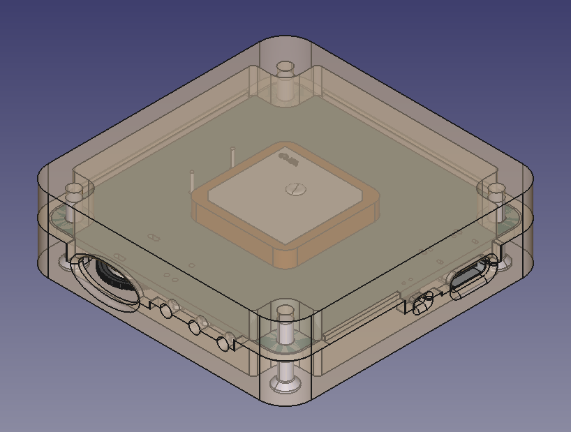
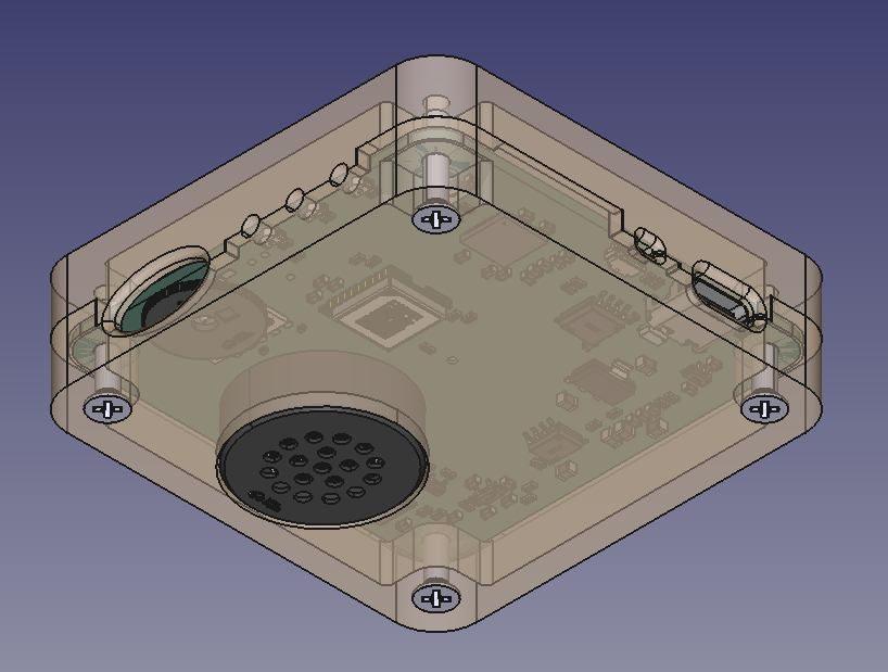
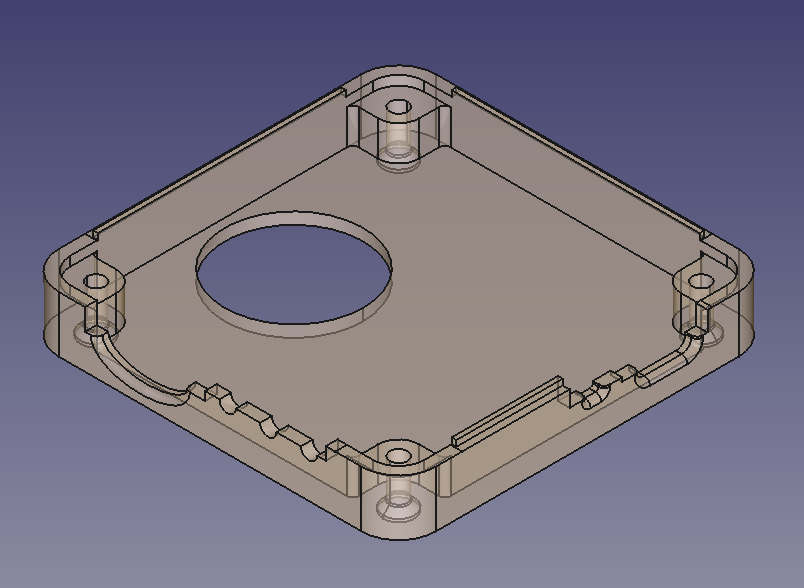
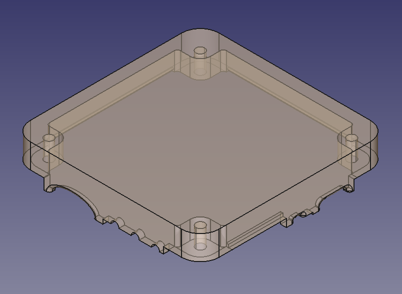
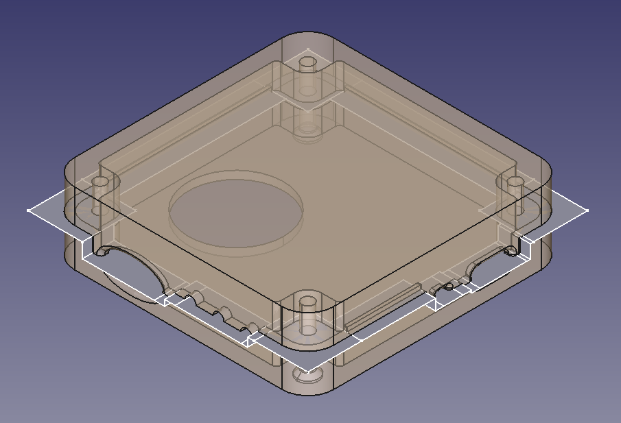
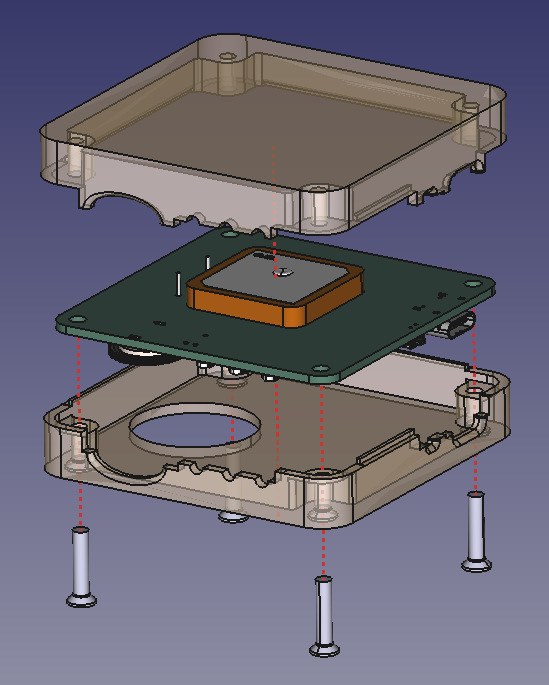
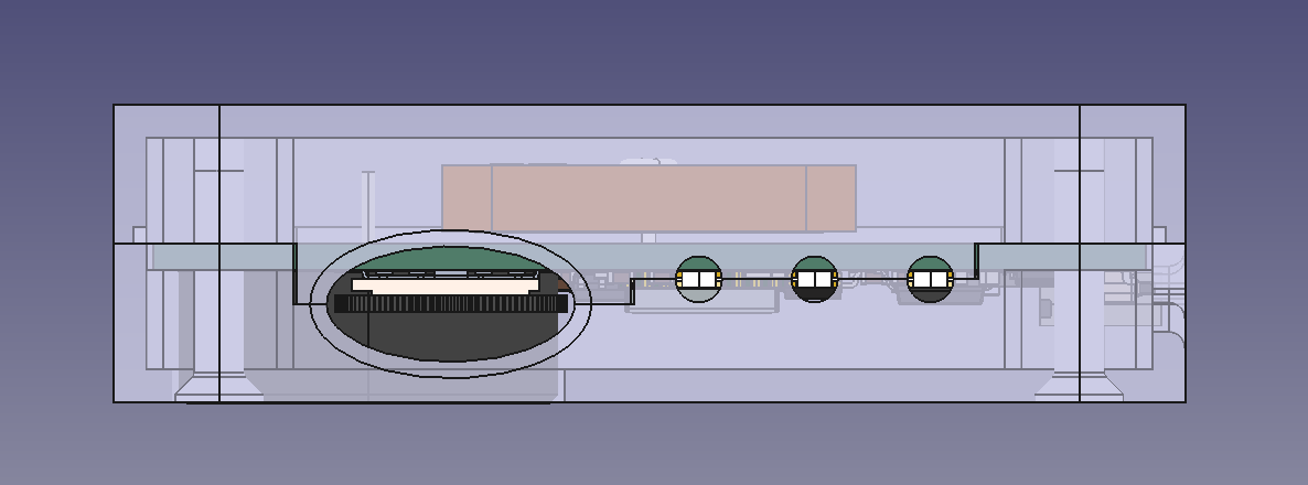
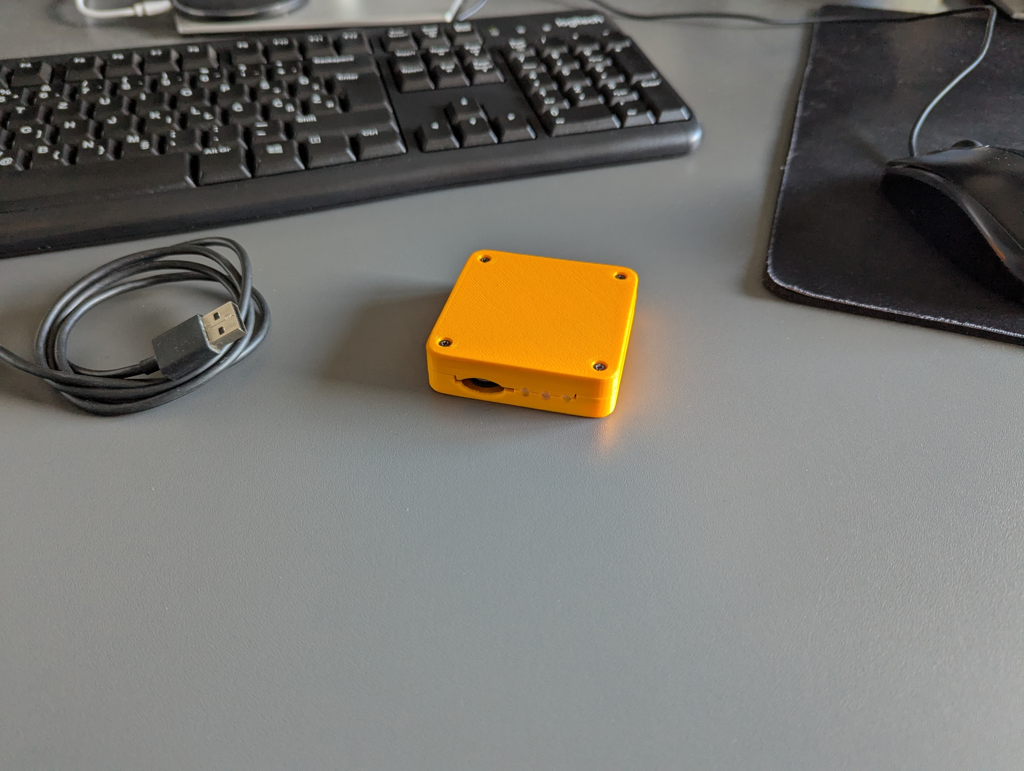
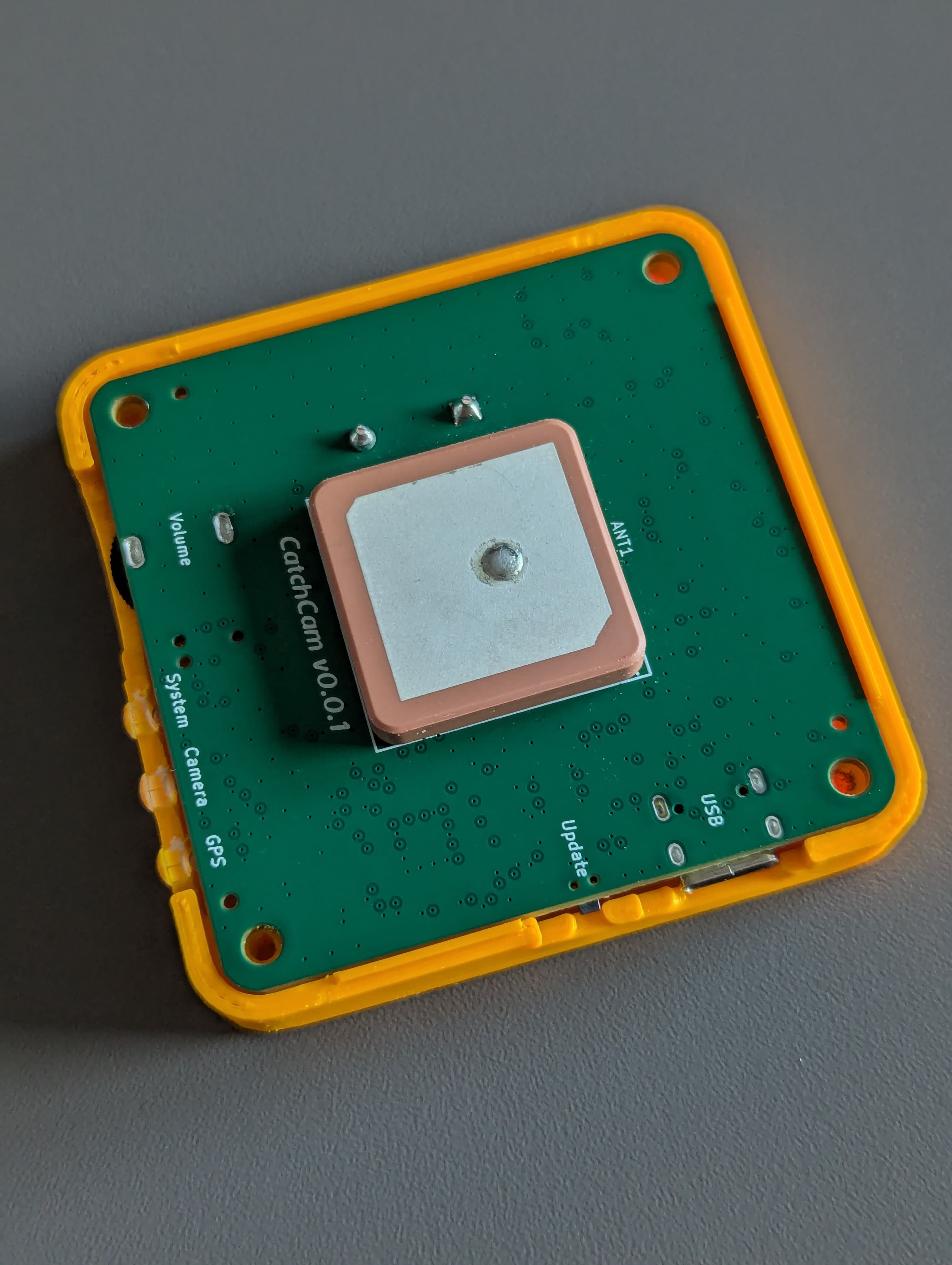
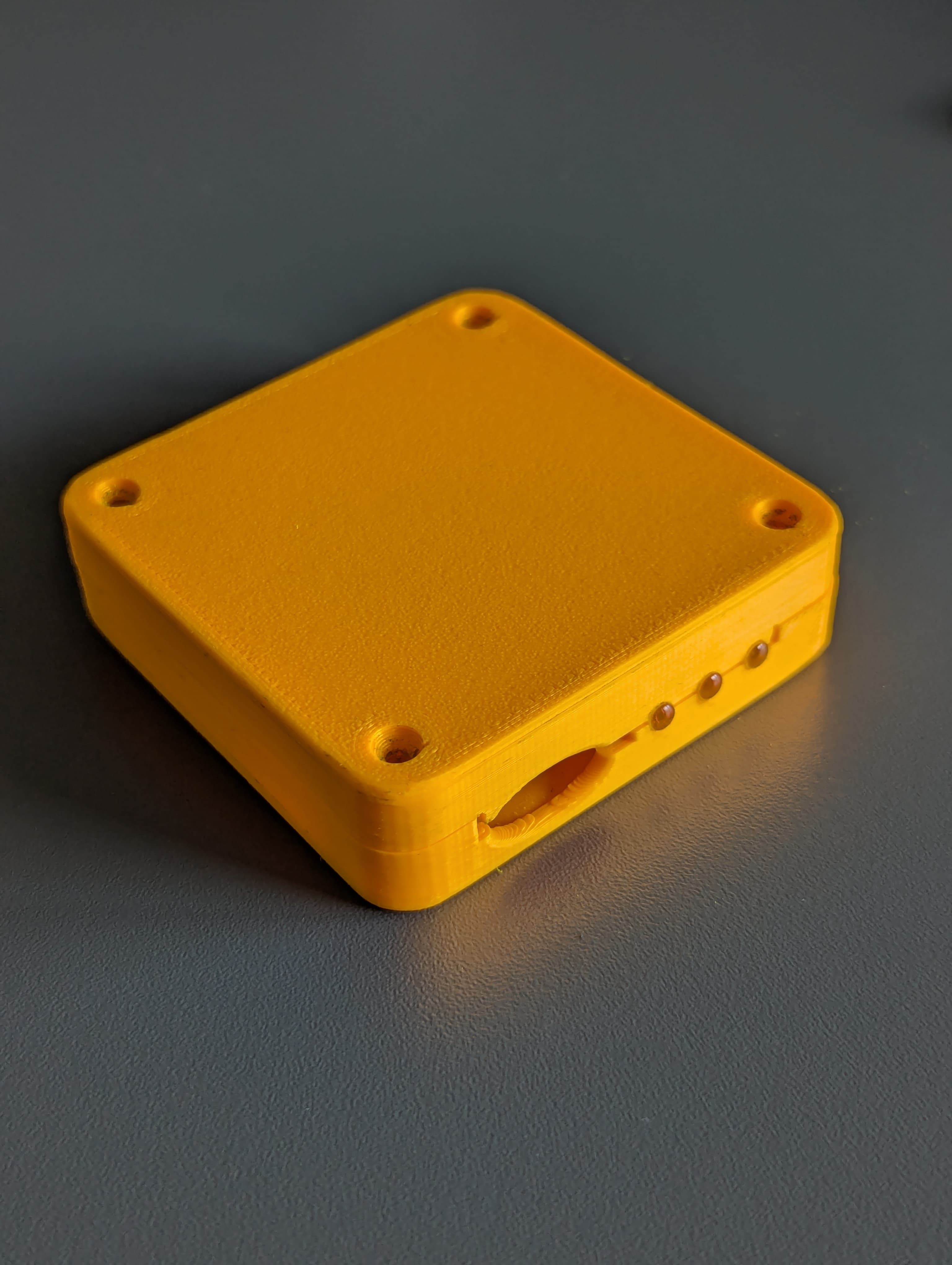
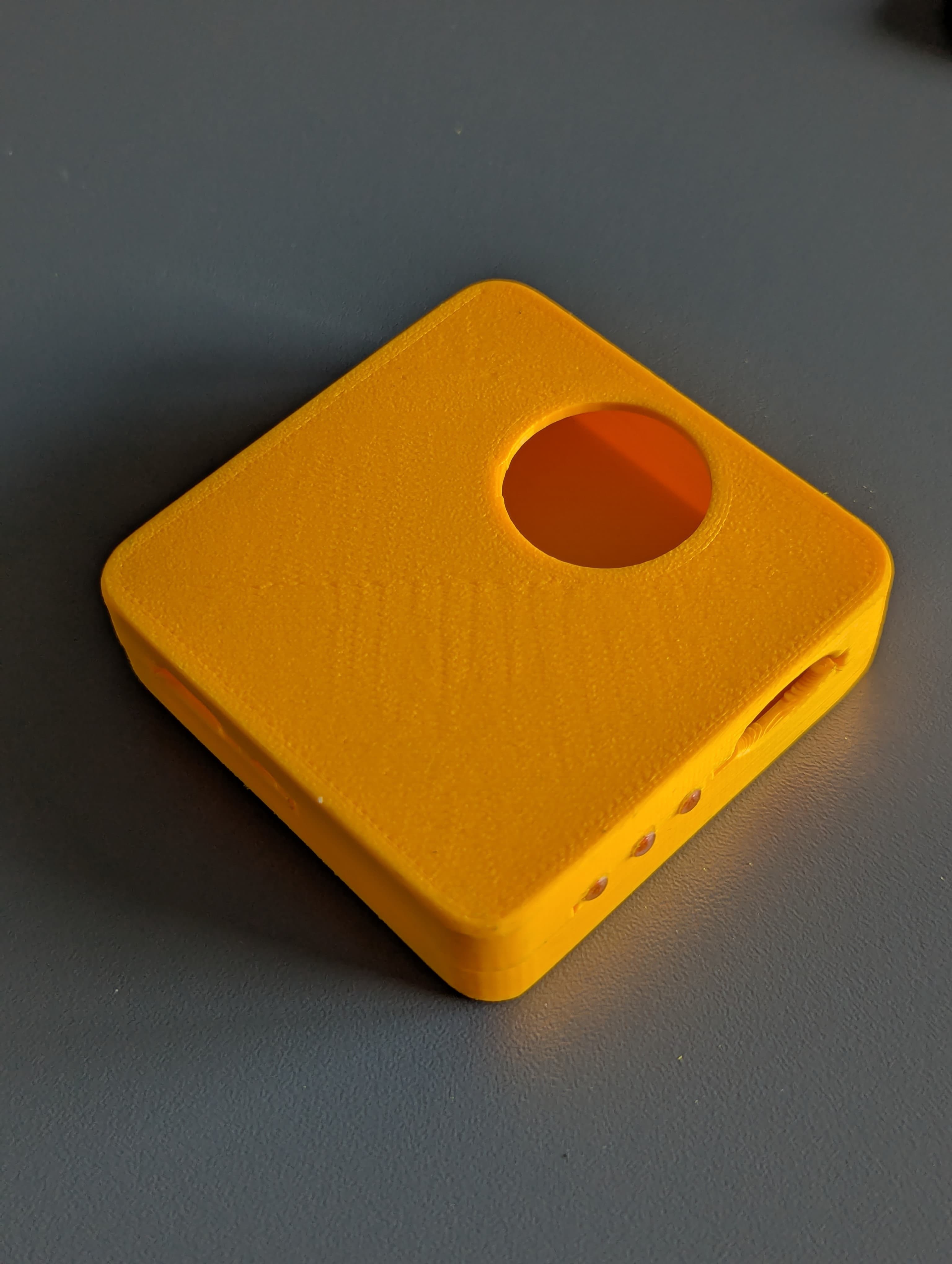
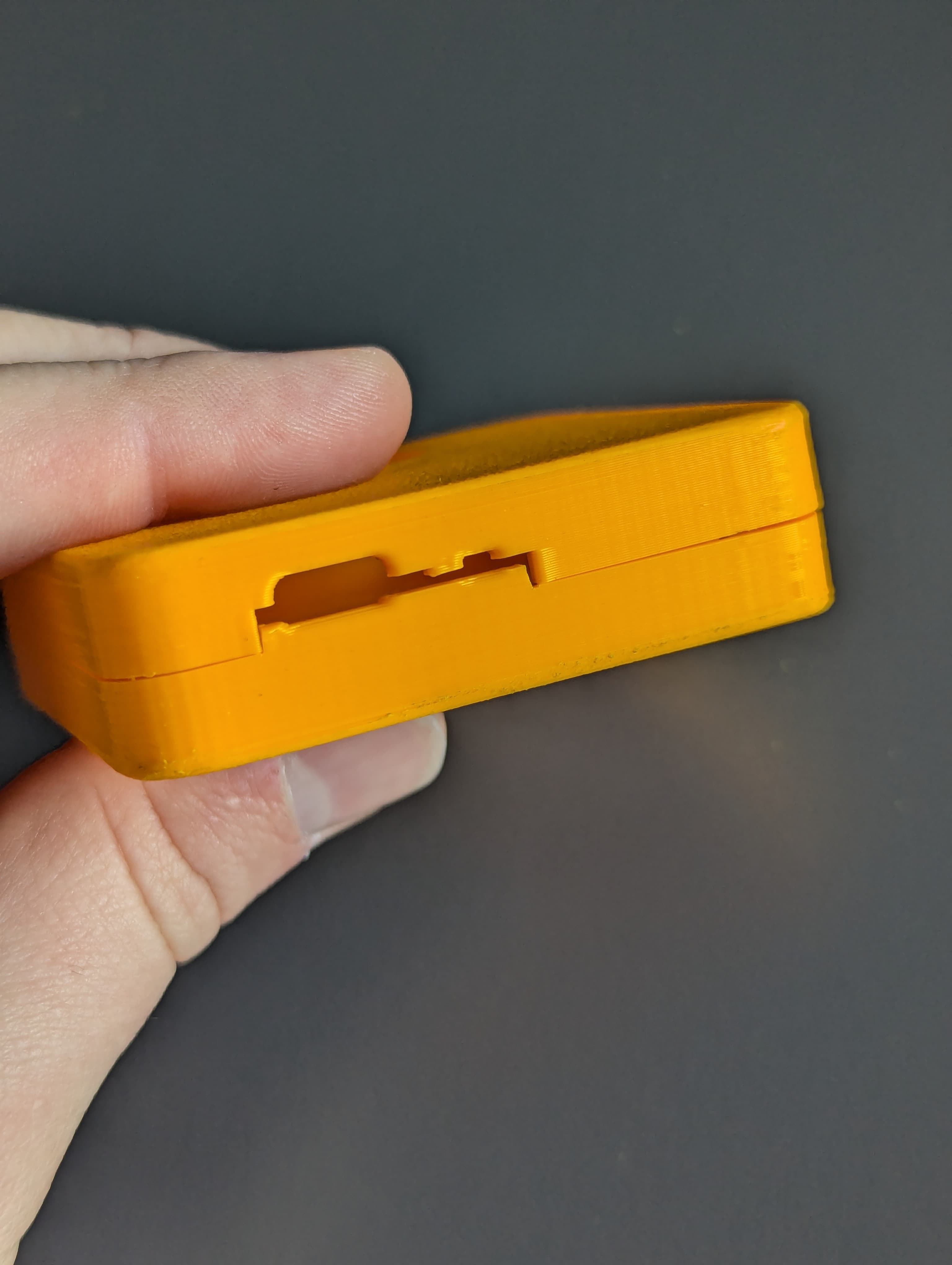
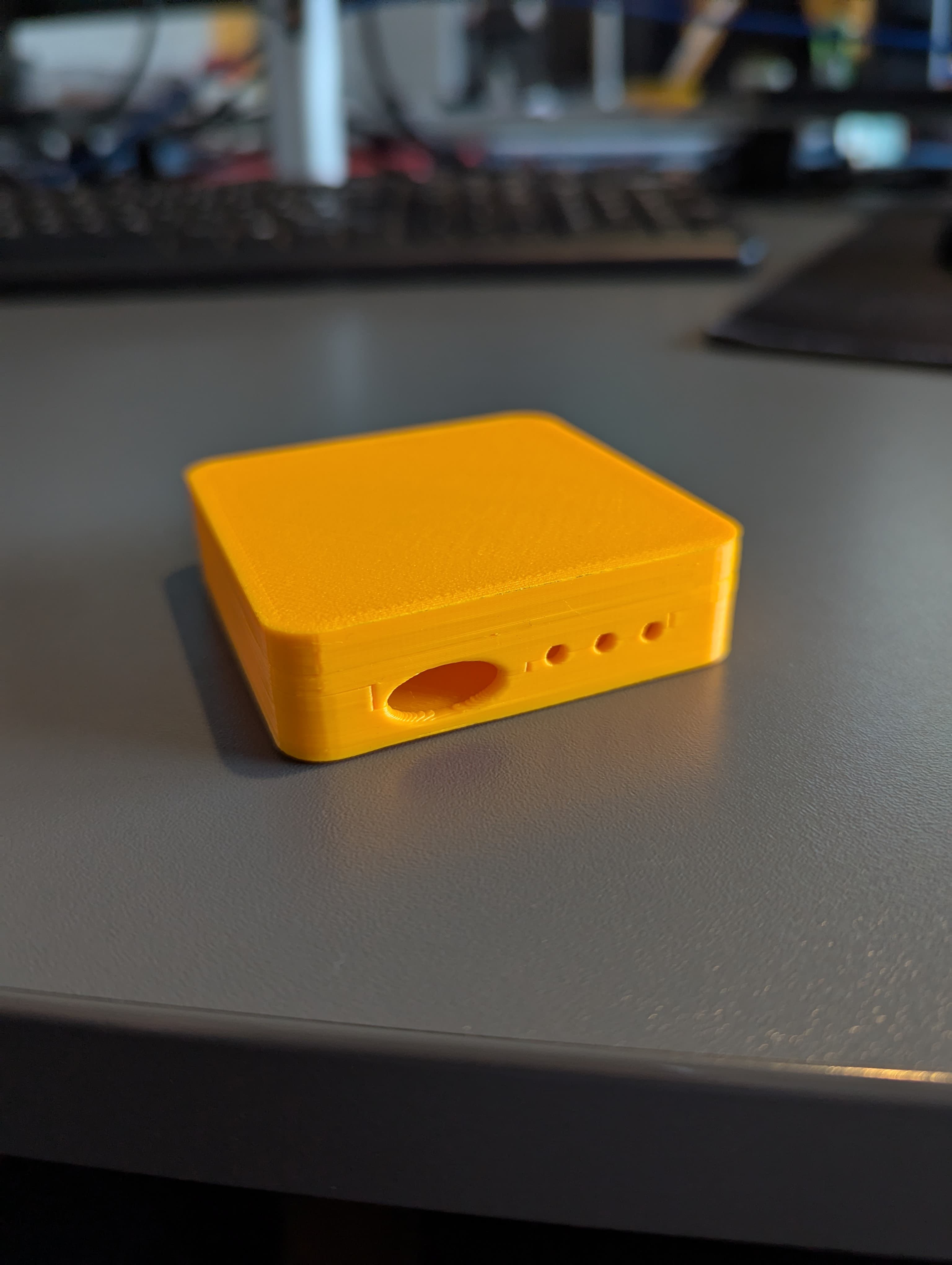
Catchcam enclosure dimensions are 65x65x18 mm. The enclosure is designed to be 3D printed in two parts: the top and the bottom part. The top and bottom dividing plane cuts trough the middle of th e USB-C, LEDs and the Volume rotary knob because those parts are sticking out of the PCB and I wanted to make assembly as easy as possible. The bottom part of the enclosure has a circular cutout for the speaker while the top part is solid. The two parts are held together with four ISO7046 M3x14 screws located in the corners of the enclosure. The enclosure will be printed in PLA, but I might try printing it in ABS or PETG for better durability.
![]()
![]()
![]()
![]()
![]()
Catchcam enclosure in FreeCAD. Design Iterations
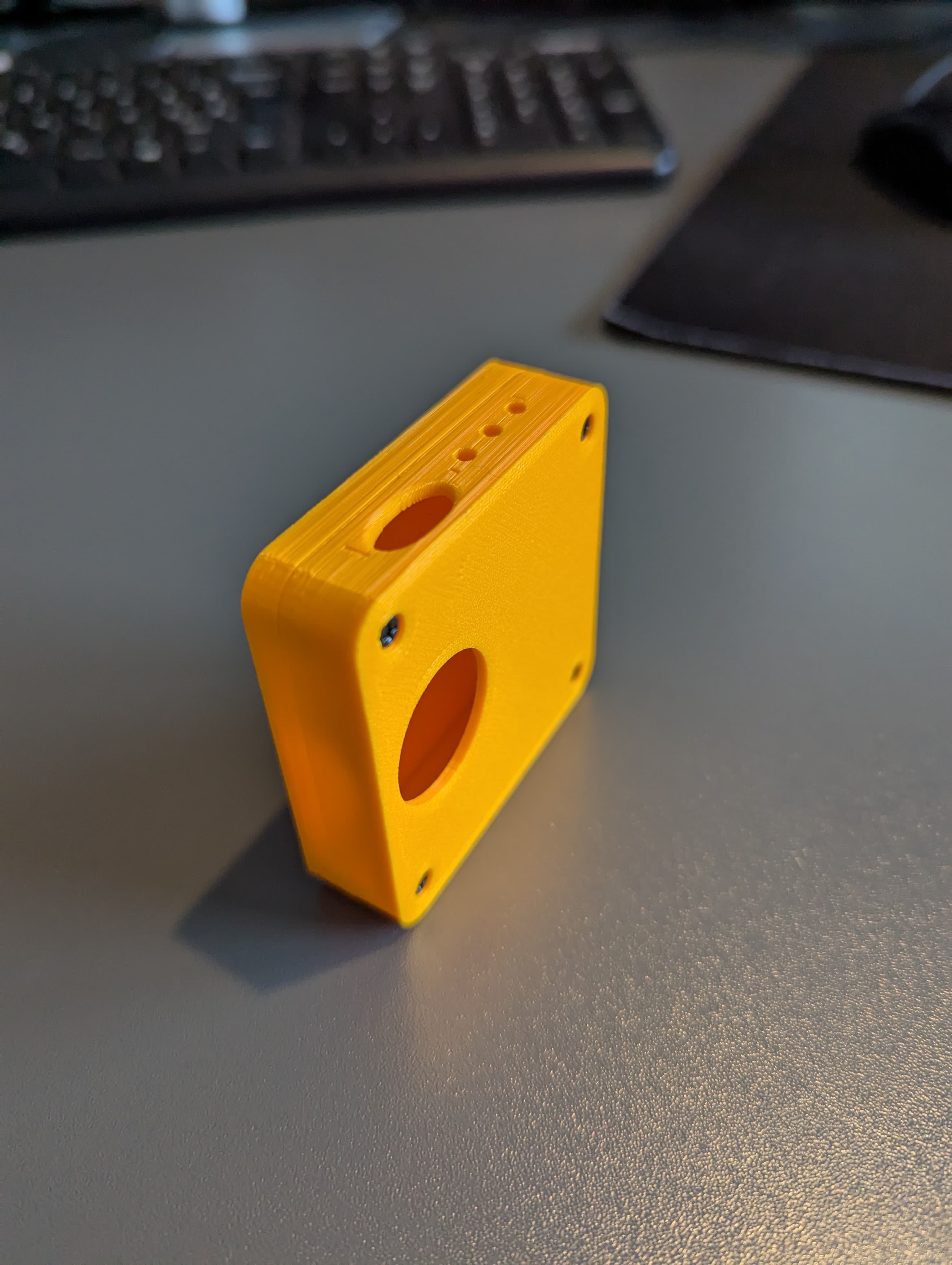
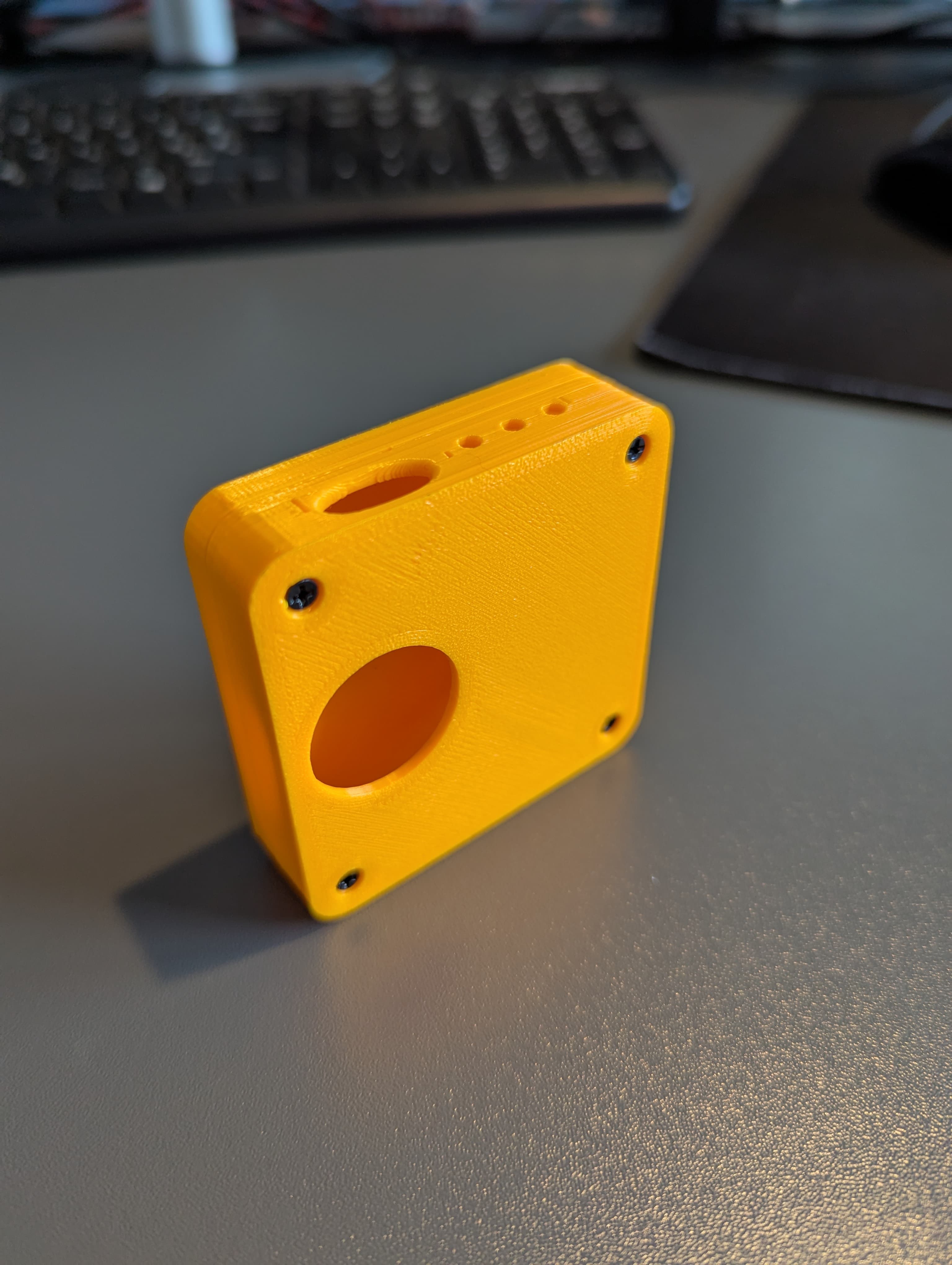
The first prototype of the enclosure had screws located at the top of the enclosure, but I’ve decided to move them to the bottom because I wanted to make the top part as clean as possible. The screw holes are designed to be self-tapping so the screws can be screwed directly into the plastic without the need for a nut. I’ve also added a small chamfer to the screw holes so the screws can be easily screwed in. For the next iteration of the enclosure, I would like to avoid using screws for assembly and try to design a snap-fit mechanism.
![]()
Catchcam enclosure exploded view. LED Diffuser Pipes
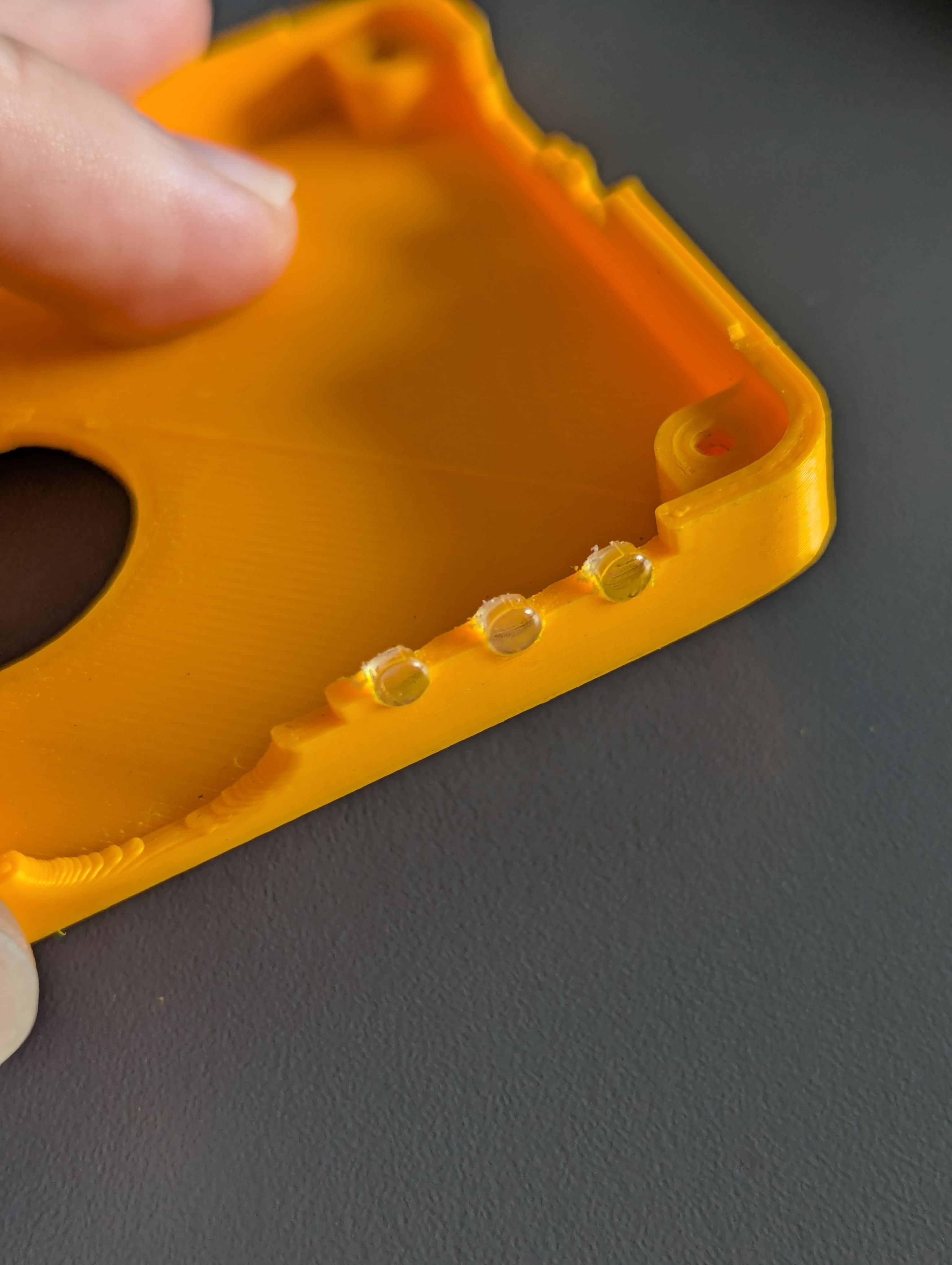
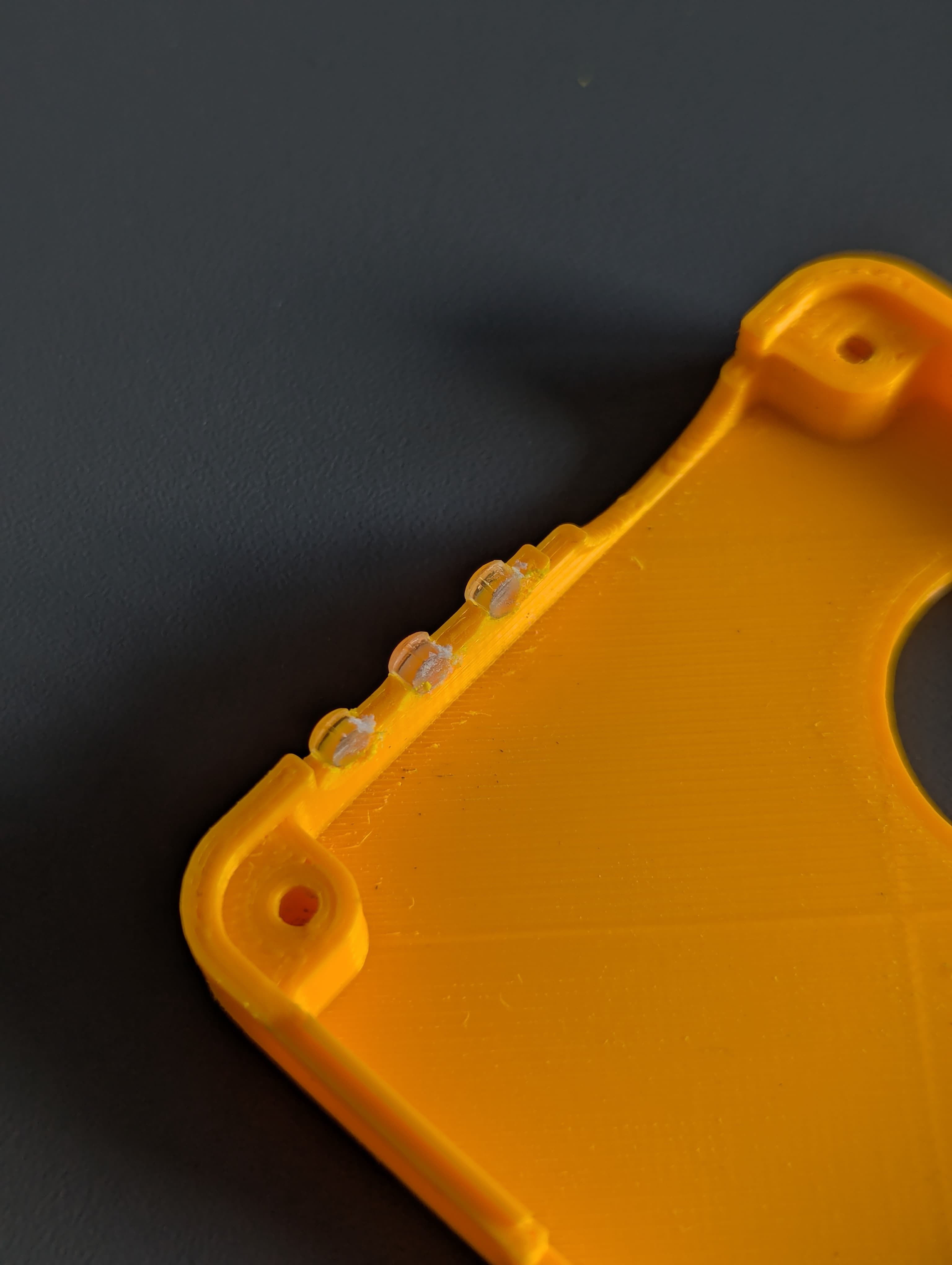
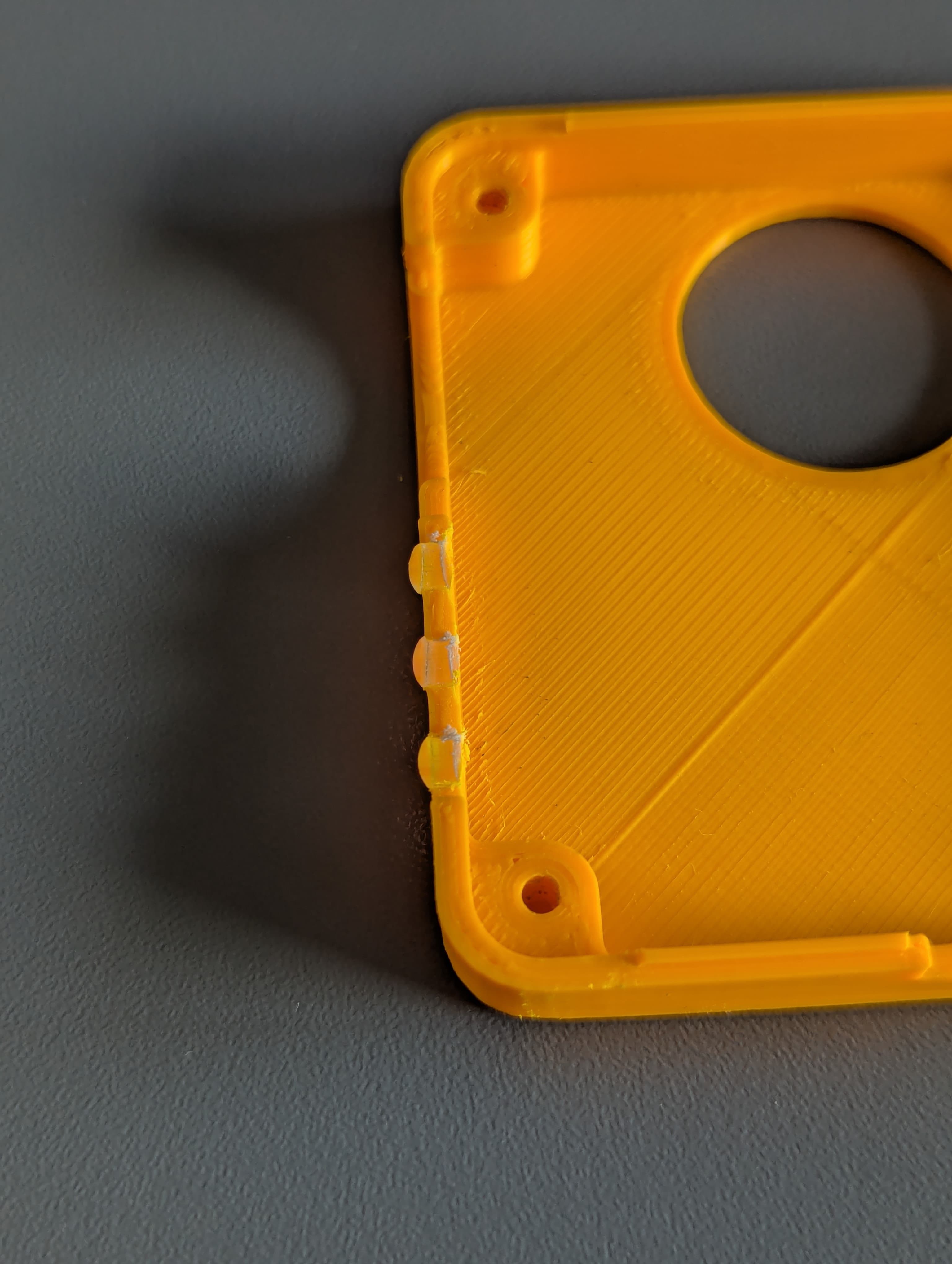
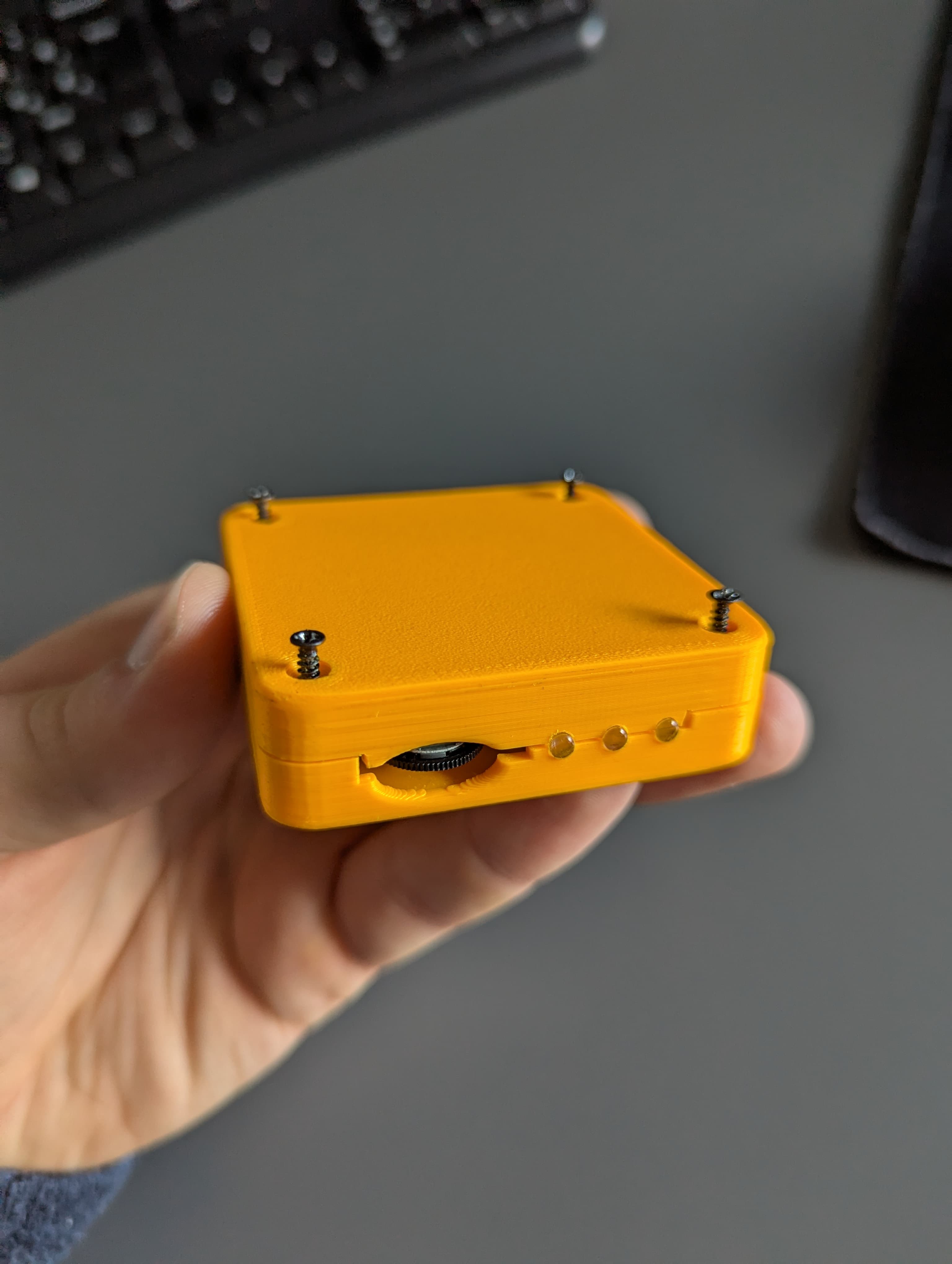
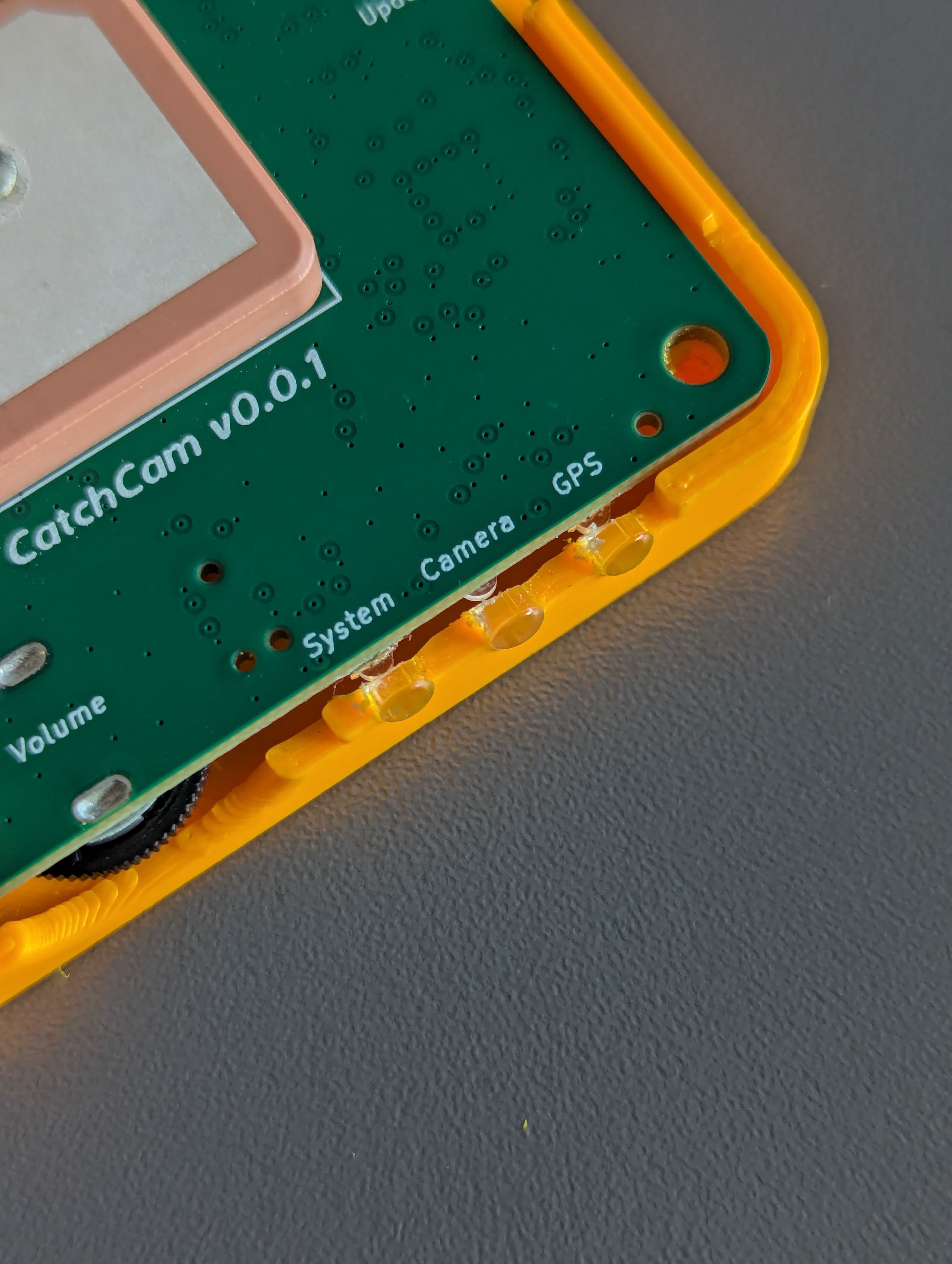
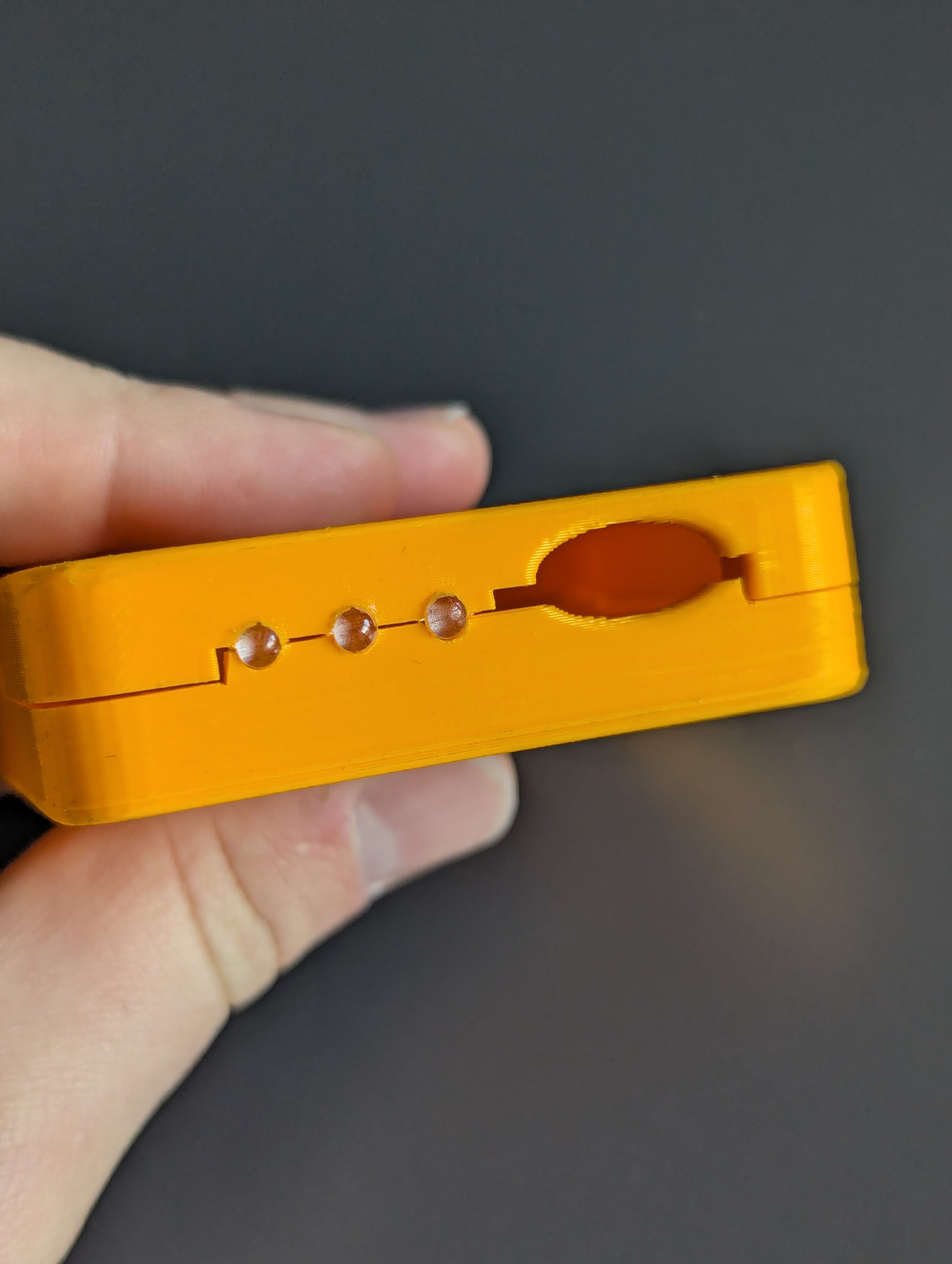
I’ve also added circular cutouts for the LEDs in order to include small plastic light diffuser pipes in order to make the LEDs more visible. The diffuser pipes are glued to the enclosure with a small amount of super glue.
![]()
![]()
![]()
Catchcam enclosure with the diffuser pipes. As you saw in the image above, the diffuser pipes holes are splitted in half for easier assembly, however, I would like to experiment with a solid hole in the future so the diffuser pipes can be pressed in without the need for glue. Moreover, I have a problem with the diffuser pipes because they are not the right length and they are interfering with the LEDs so I need to grind them down a bit in order to make them fit nicely.
Antenna Considerations
I’ve especially paid attention to the distance between the PCB and the top part of the enclosure because of findings in the Molex GPS Ceramic Antenna application specification document where the GNSS antenna performance can be affected by the distance between the antenna and the ground plane. Currently, the distance is around 6.37 mm and that seems to be working fine.
![]()
Catchcam enclosure with the GNSS antenna. 3D Print and Assembly
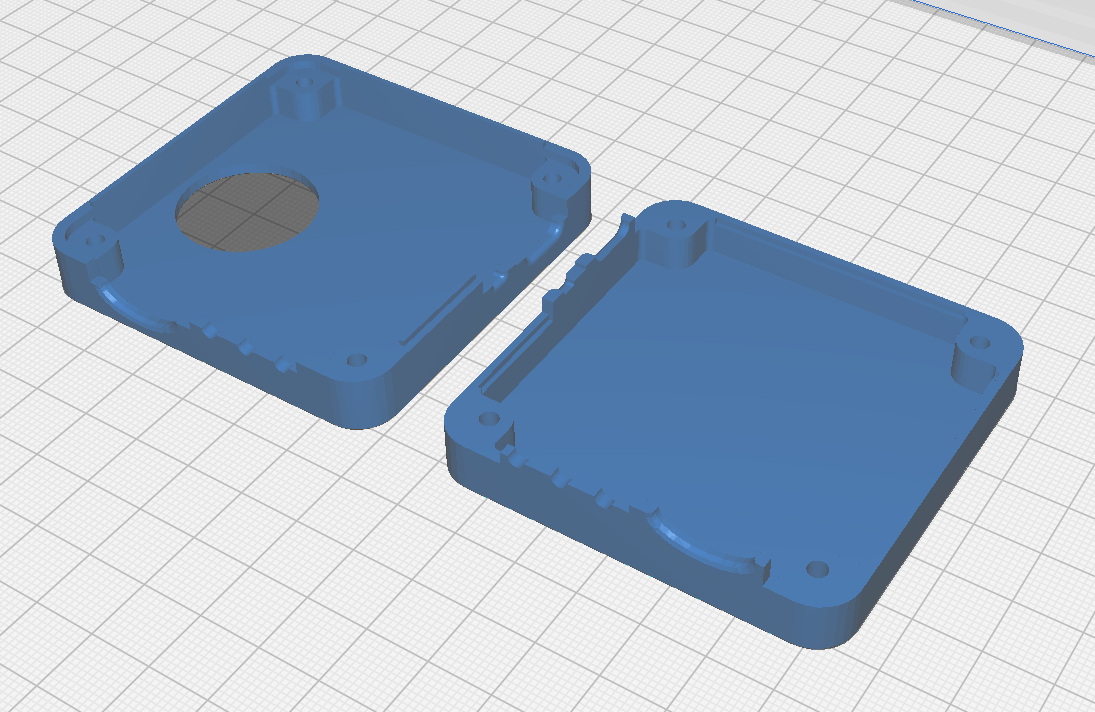
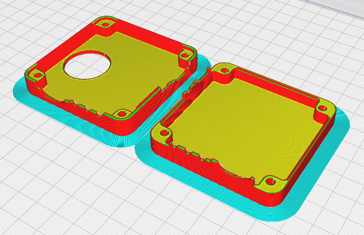
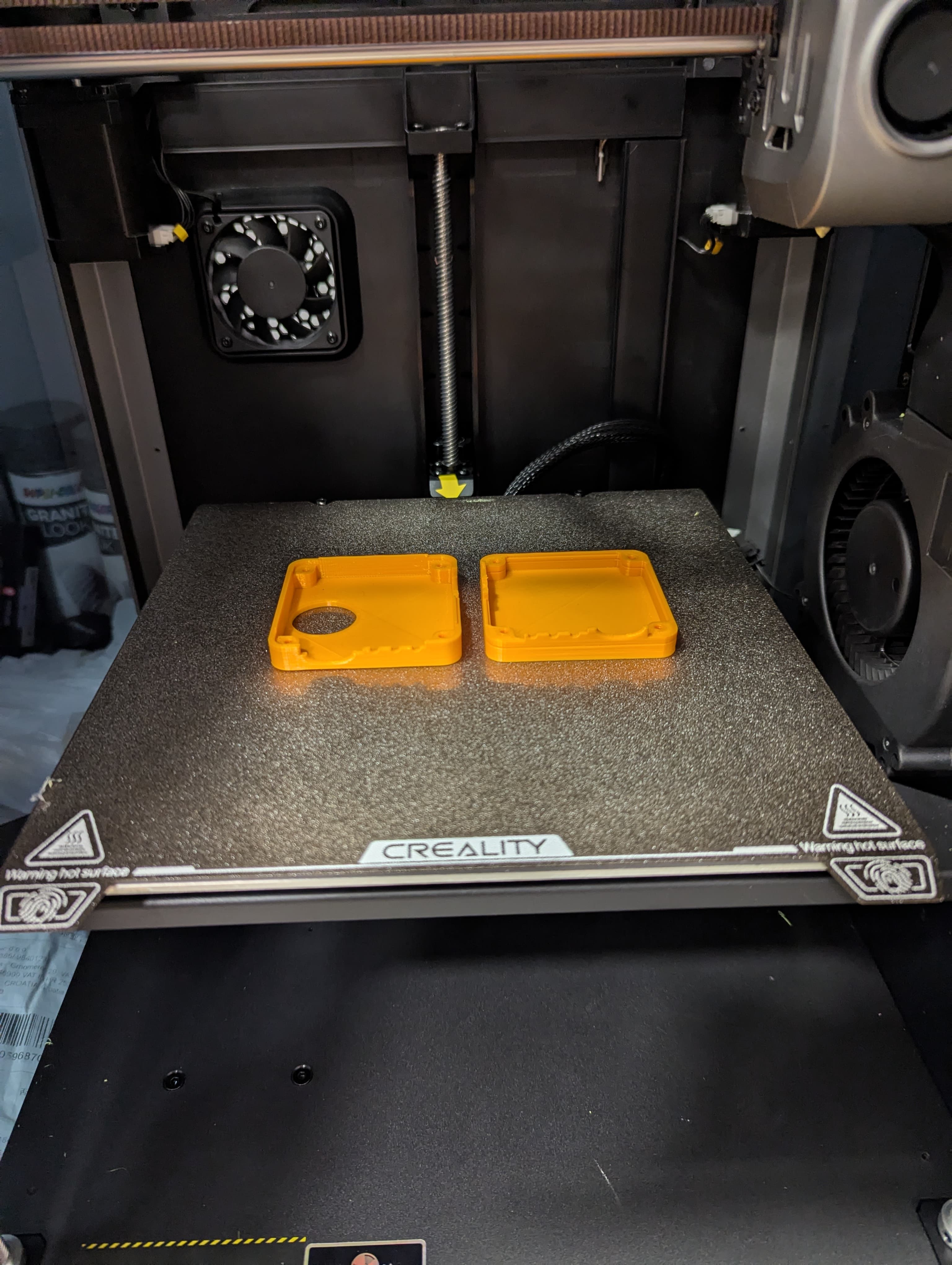
The top and bottom parts of the enclosure are meant to be printed on the largest surface placed on the print bed in order to avoid printing unnecessary support material. As for the 3D design guidance, I’ve used the UltiMaker Cura slicer software so I could see how the model would be sliced and printed.
![]()
![]()
Catchcam enclosure in UltiMaker Cura slicer. Note the orientation of the top and bottom enclosure parts. 3D print came out quite nicely, although I had some problems with the first print because the printer was not calibrated properly (you can see missing walls around cutouts). Also, the fit was rather tight, so I had to grind down the edges a bit in order to make the assembly easier.
![]()
![]()
![]()
![]()
![]()
![]()
![]()
![]()
![]()
![]()
![]()
![]()
![]()
![]()
![]()
![]()
![]()
![]()
![]()
![]()
![]()
![]()
![]()
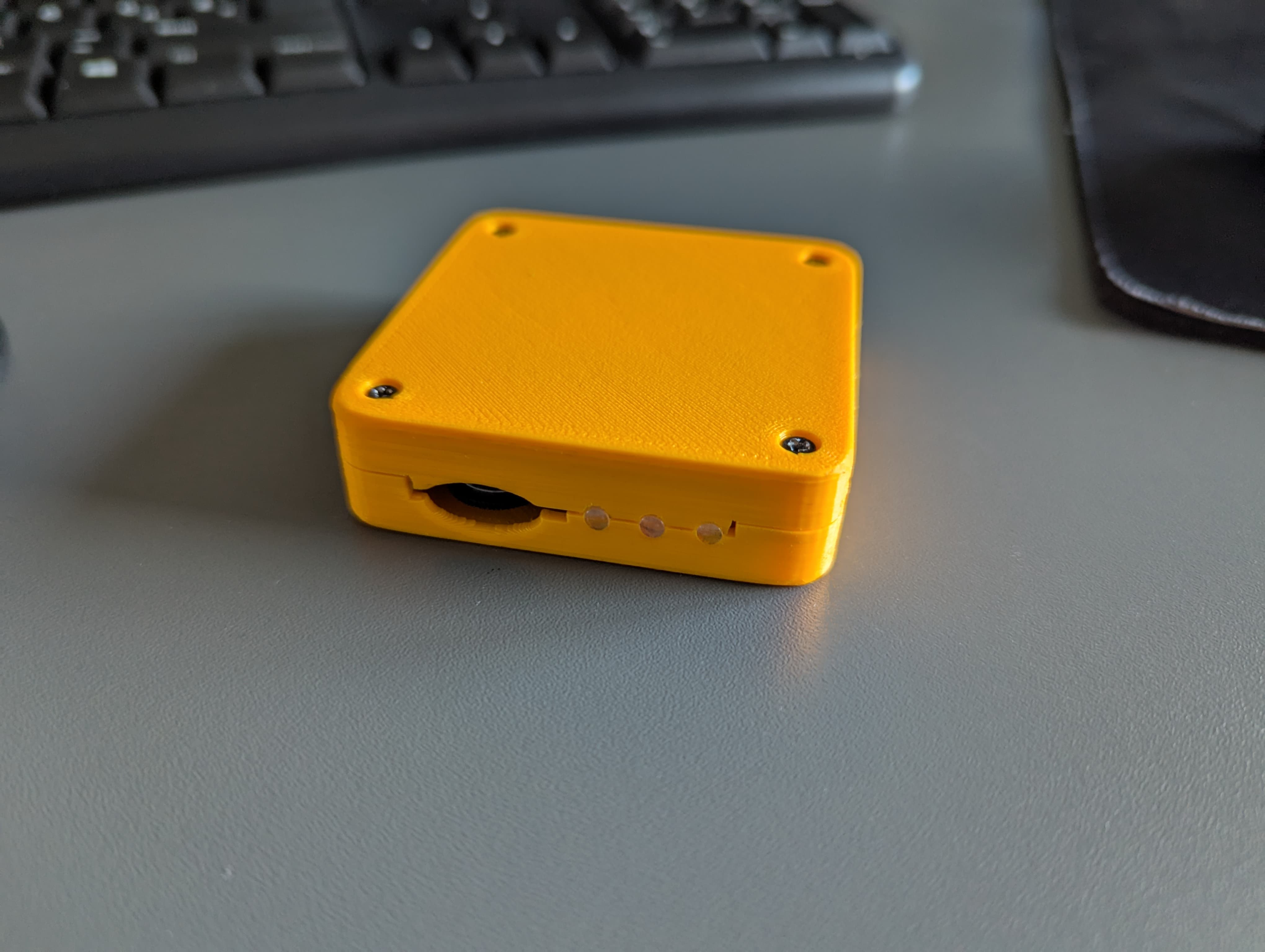
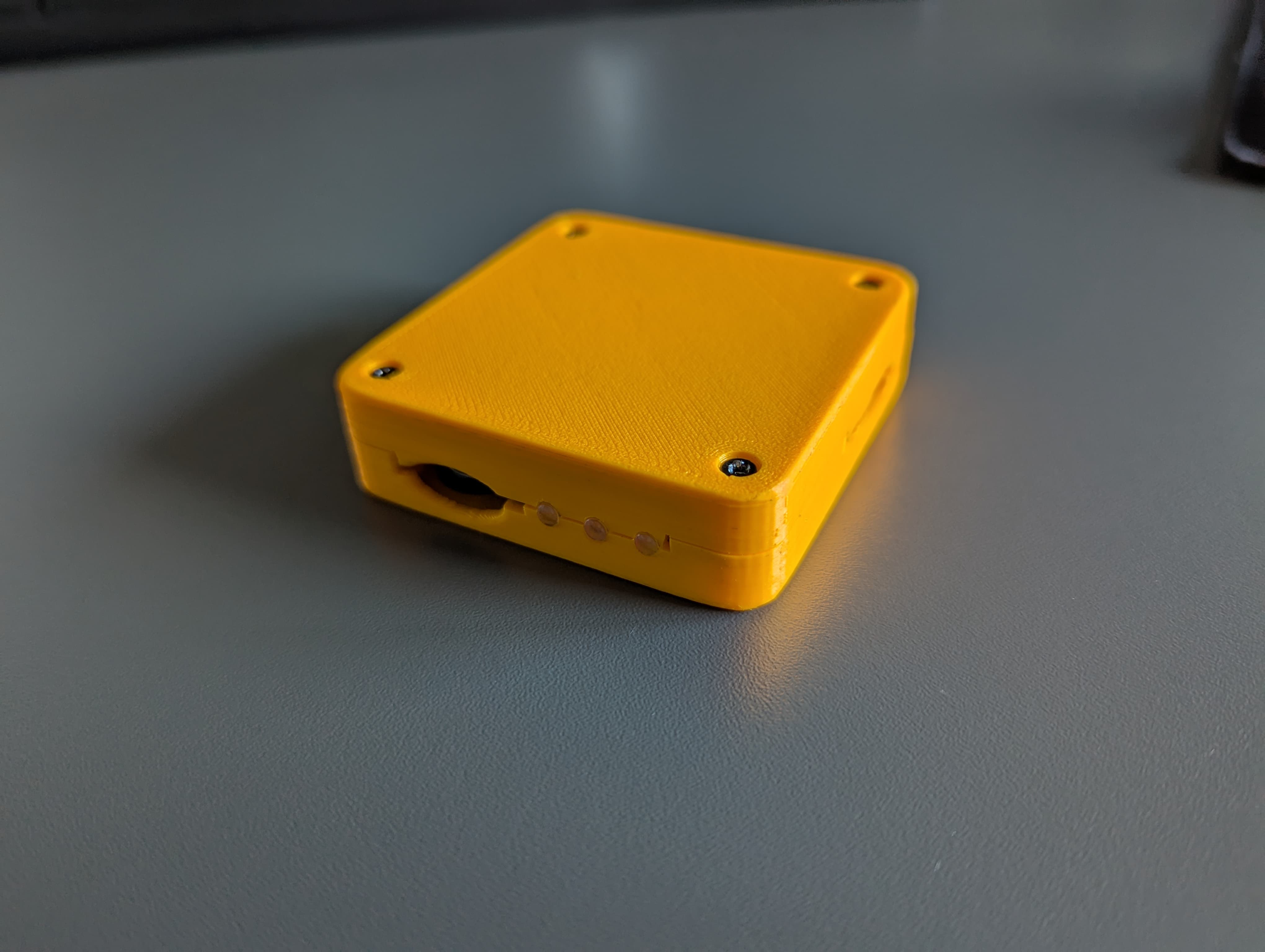
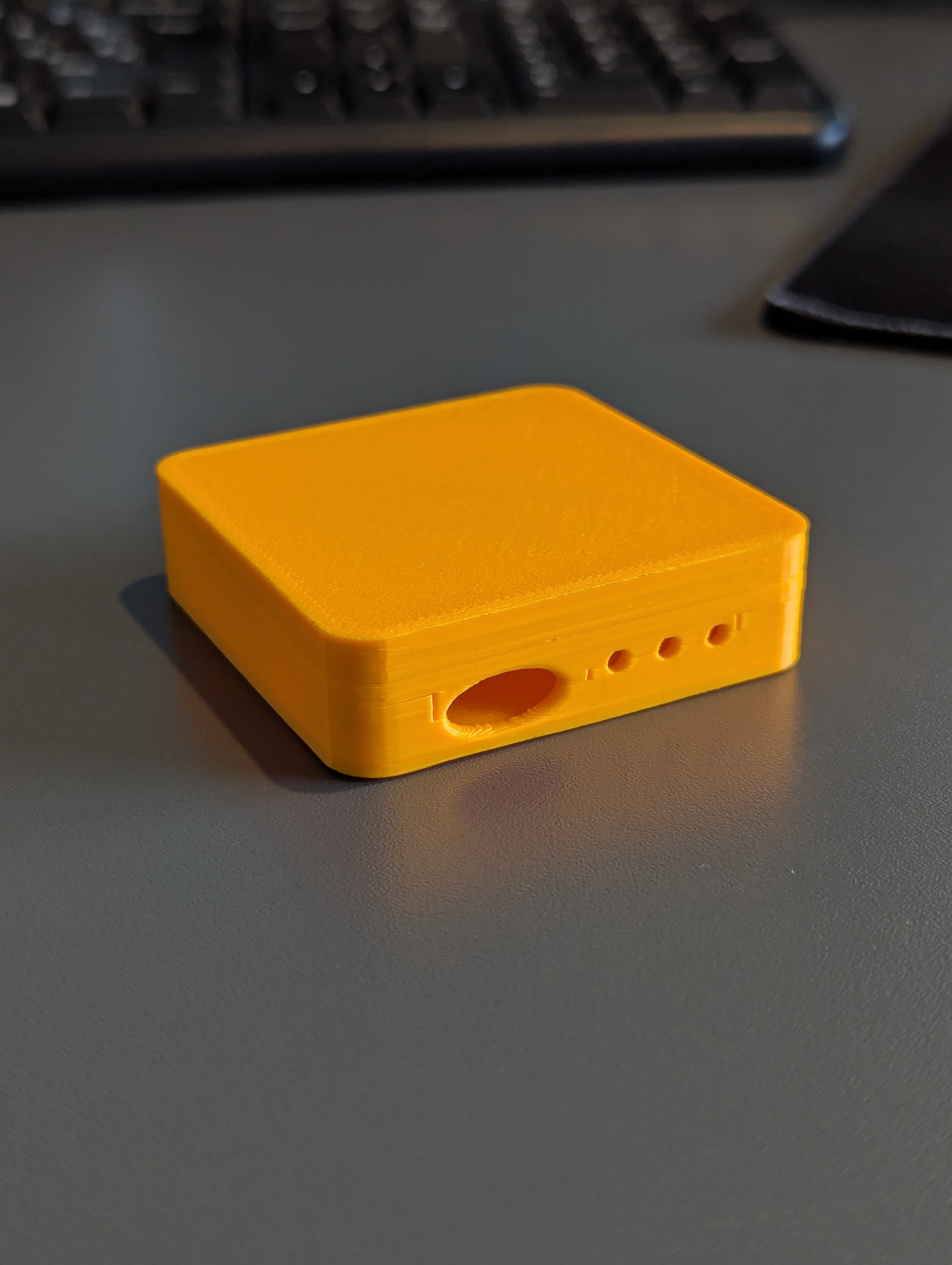
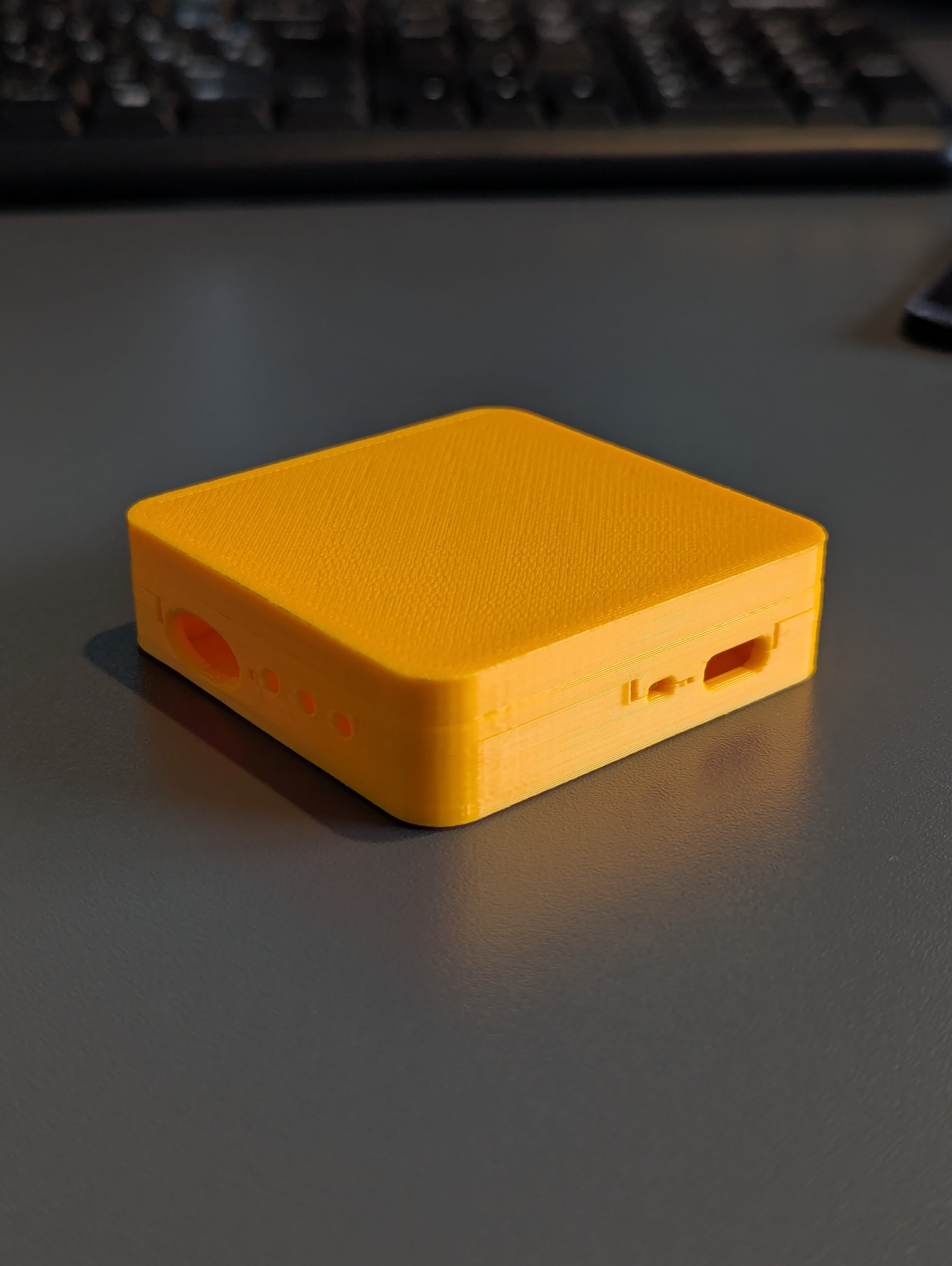
First Catchcam enclosure 3D print. The second print came out much better and the fit was still tight, but I didn’t have to grind down the edges. Also, the walls around the cutouts were printed properly. Note that the screws are now on the bottom side of the enclosure.
![]()
![]()
![]()
![]()
![]()
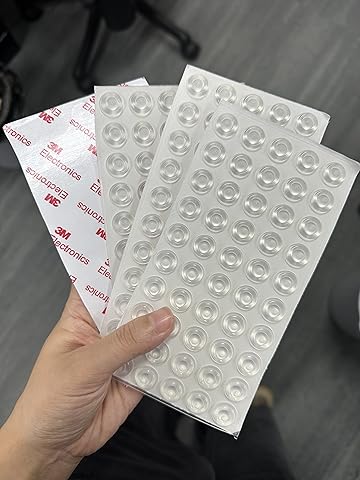
Second Catchcam enclosure 3D print. The last step of the process would be to attach four rubber feet to the bottom of the enclosure in order to prevent it from sliding off the surface. I haven’t decided on the type of rubber feet yet, but I’m thinking about using self-adhesive rubber feet that are commonly used for furniture if I could find them in the right size.
![]()
Rubber feet. Courtesy of amazon.com. Future Plans
I don’t like how the Volume rotary knob is not sticking enough out of the enclosure, so I would like to make it stick out a bit more in the future. I haven’t managed to find a suitable knob with larger knob diameter and maybe a redesign of the PCB would be necessary. Maybe I can “extrude” the part of the PCB where the rotary knob is located so it sticks out more. I wouldn’t want to do that actually because I like the rectangular shape of the PCB. In order to make knob adjustment easier, I’ve made quite a large cutout so the thumb finger can easily reach the knob.
![]()
Rotary knob cutout. I’m thinking about spray painting the enclosure in the future in order to make it look more professional and to protect the PLA from UV light. Later, I would like to laser engrave the logo on the top part of the enclosure with the name of the project, and add labels for the LEDs and the Volume rotary knob. I presume that the laser would burn the spray paint and reveal the PLA color underneath.
Conclusion
I’m quite happy with the enclosure design and the way it turned out. The design is simple, clean, and functional. The assembly is easy and straightforward. I’m looking forward to testing the enclosure with the final version of the PCB and making any necessary adjustments
Note: If you’re interested, you can pre-order a sample at vnucec.ivan@gmail.com.
-
Designing GNSS Circuitry
11/25/2024 at 10:04 • 0 commentsIn this post, I will discuss the design and implementation of the GNSS circuitry for my Catchcam project.
If you haven’t already, I recommend reading my previous post on Catchcam: Choosing Components to get some background on the component selection process. In that post, I discussed my decision to use the
SIM68MGNSS module and theKH-GPS252504-WYCeramic Patch antenna for my project. In this post, I’ll dive deeper into the design and implementation of the GNSS circuitry.Note: If you’re interested, you can pre-order a sample at vnucec.ivan@gmail.com.
GNSS Module
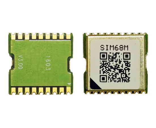
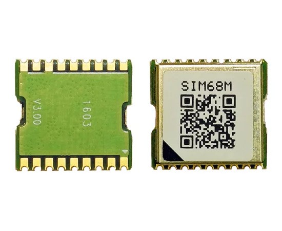
SIM68Mis quite a simple GNSS module. It is powered by a 3.3V supply, has a built-in LNA, supports both active and passive antennas, and communicates over UART using the NMEA protocol.![]()
SIM68M GNSS module. Courtesy of micros.com. However, I’ve encountered a couple of issues during implementation.
The datasheet specified a baud rate of 115200 (see the image below), but in reality, the module operated at 9200 baud. However, this was not a big issue, because the baud rate can be easily configured by sending the appropriate AT command over UART.
![]()
SIM68M Baud rate as stated in the datasheet. Additionally, the datasheet lacked information about the part orientation in the reel, leading to assembly problems at JLCPCB. I’ve had to opt for manual inspection option, which added a small extra cost. Other than that, I am quite pleased with the performance of the module.
Antenna
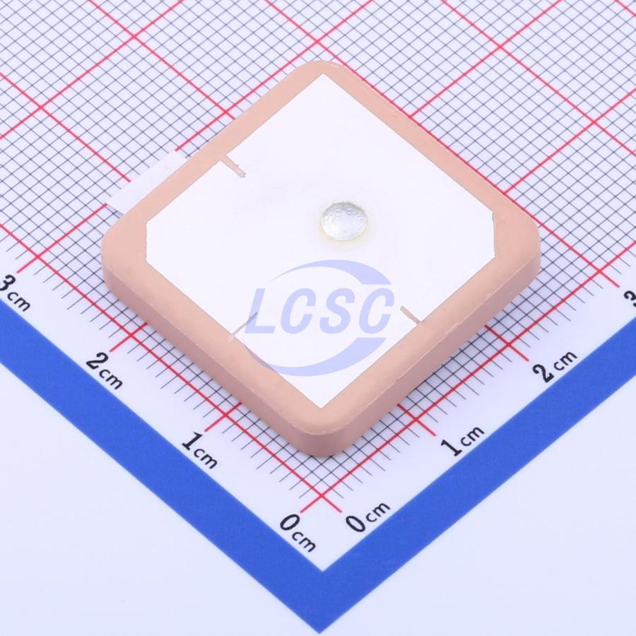
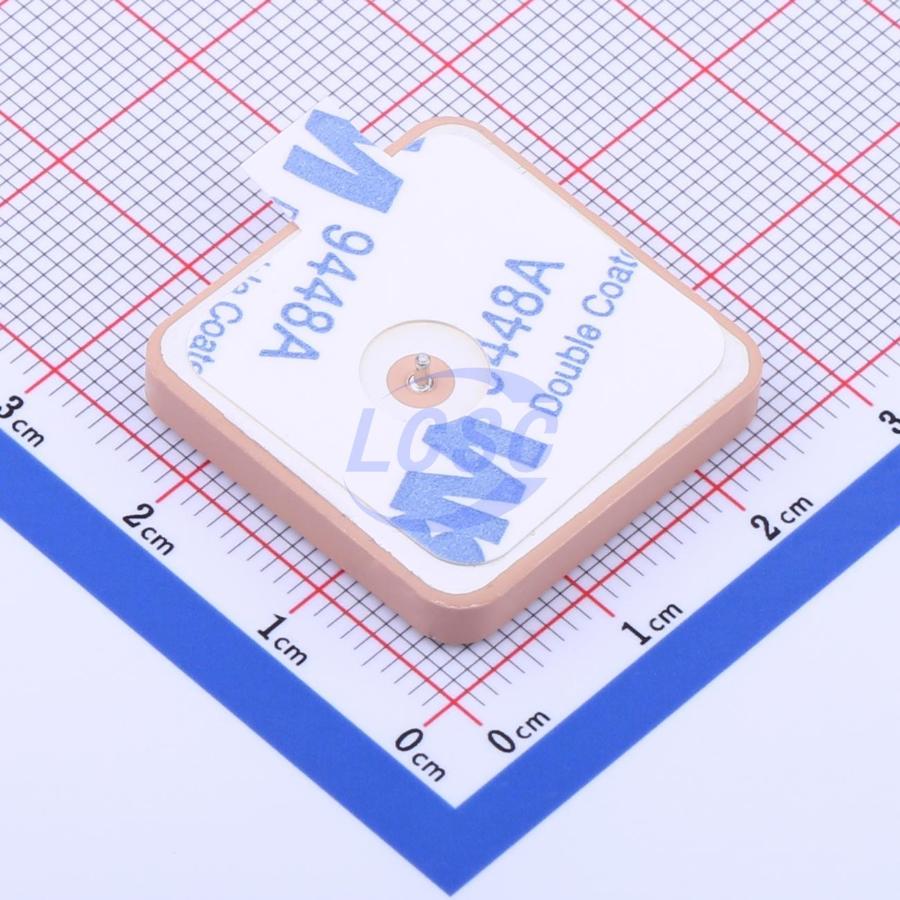
I’ve decided to go with the 25x25 mm
KH-GPS252504-WYGNSS antenna.![]()
![]()
KH-GPS252504-WY GNSS Ceramic Patch antenna. Courtesy of lcsc.com. It was really cheap one, although the datasheet is a bit lacking when it comes to the recommended ground plane size (more on that later). I reached out to the manufacturer for some clarity, and their customer support was surprisingly helpful. They told me a 60x60 mm ground plane would do the trick, but they didn’t really explain why. Still, they were generous enough to offer 10 free samples for our project, which was a nice gesture.
PCB Design
I’ve chosen
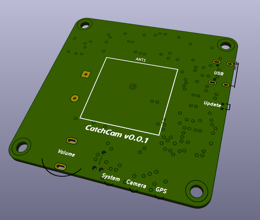
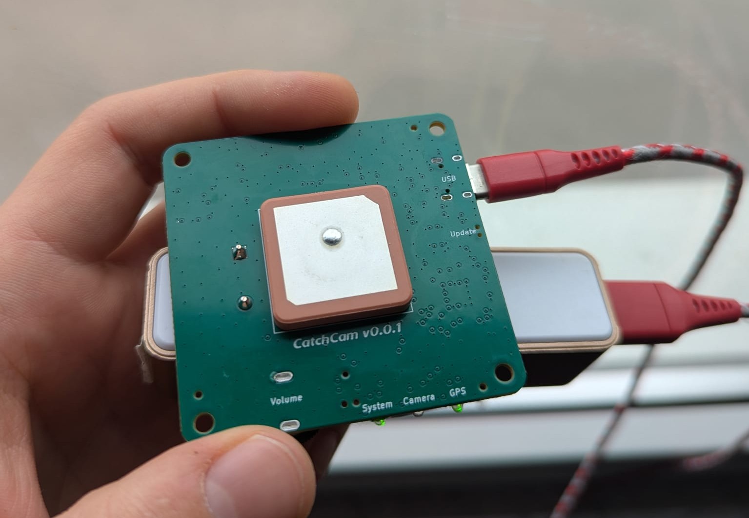
GND - SIG/PWR - SIG/PWR - GNDstackup for my 4-layer PCB because the GNSS Antenna needs a solid ground plane beneath it to work properly. Antenna is placed on the top side, while the GNSS module and the rest of the system circuitry is placed on the bottom side. This way, the antenna feed pin is as close as possible to the module in order to minimize PCB signal loss and interference. The stackup I’ve chosen is not ideal because the inner signals are not shielded by the ground planes as they would be in a more popularSIG/PWR - GND - GND -SIG/PWRstackup. The ground size is set to 60x60 mm, as recommended by the antenna manufacturer.![]()
PCB from the Top side. Note that the antenna is the only part populated on the top side. I couldn’t manage to get 50 Ohm impedance on the GNSS signal trace with the chosen stackup (they were exceeding 1 mm in width), but I’m not too worried about it because the trace lengths are much shorter than the GNSS signal wavelength. I’ve also added a Pi matching network footprints to the PCB, and added 0 Ohm resistor so I can to tune the signal trace later.
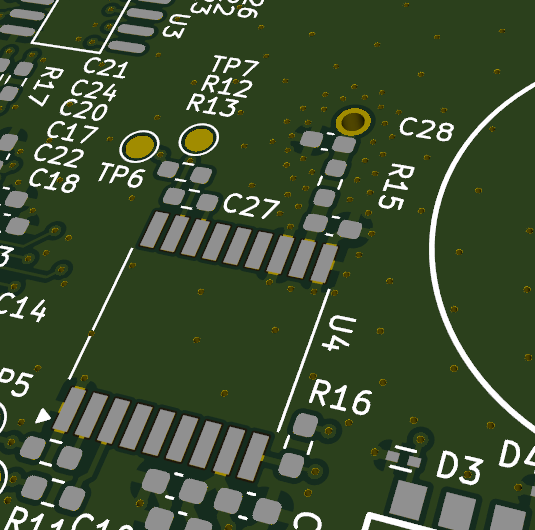
![]()
Antenna, matching network, and GNSS module footprints as seen from the bottom side. I’ve spaced out any other trace or component that might potentially interfere with the GNSS signal. I’ve surrounded the GNSS signal trace with lots of ground stitching vias to create a signal waveguide in order to minimize interference.
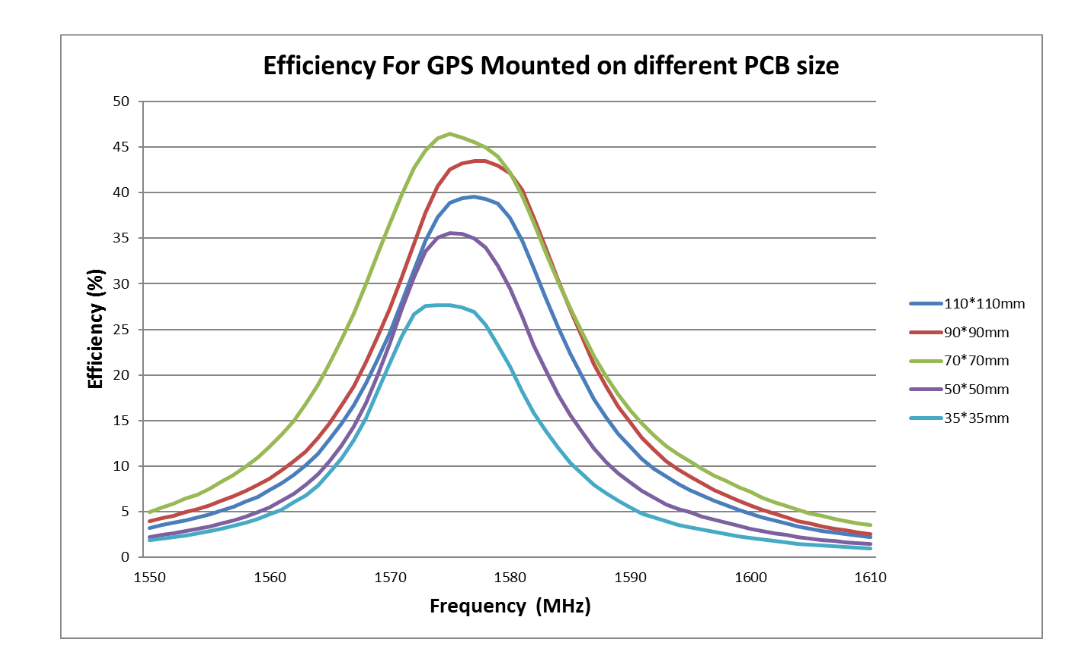
Note that the antenna resonant frequency (and efficiency) shifts with different ground plane sizes as shown in this Application specification, and depending on the size of the antenna and the PCB, there is a sweet spot where the antenna efficiency is the highest. In my case, I had to guess because the datasheet didn’t provide any information on the ground plane size.
![]()
Antenna efficiency versus different PCB sizes. Curtesy of tools.molex.com. I would like to mention a nRF9161-dk reference design, which was quite helpful in designing the GNSS circuitry. Also, the ANR017 GNSS ANTENNA SELECTION guide helped me understand that the best way to place a GNSS antenna is in the middle of the PCB and with a solid ground plane beneath it.
Testing
Antenna performance
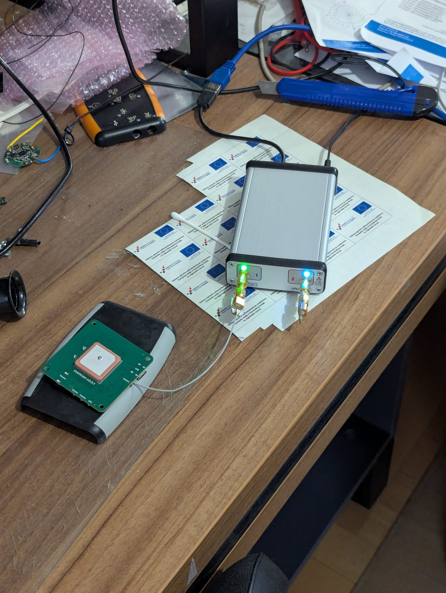
After the boards arrived, I’ve measured the antenna characteristics using the
MegiQ VNA-0460VNA by soldering a coaxial cable to the antenna feed pin.![]()
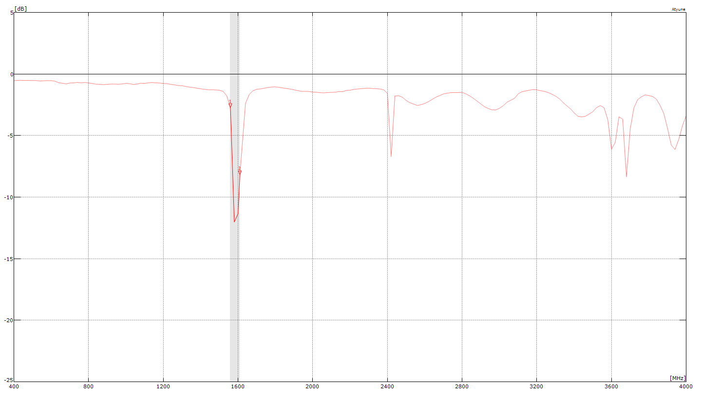
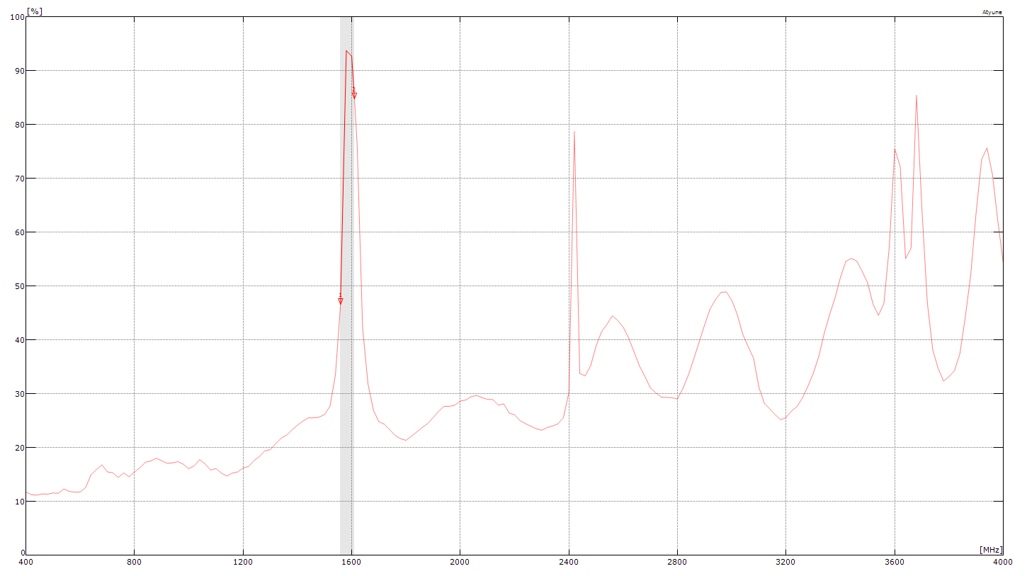
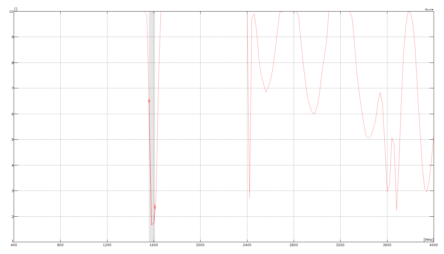
Measuring antenna performance using VNA. The results were quite promising as you can see in the images below (note that the GNSS L1 band is grayed out).
![]()
Antenna Return loss measurements. ![]()
Antenna Efficiency measurements. ![]()
Antenna Voltage Standing Wave Ratio (VSWR) measurement. Antenna has a return loss at around -12 dB, which is quite good. The efficiency is around 93% at the resonant frequency, which is also quite good. The VSWR is around 1.6. Overall, I’m quite pleased with results even without the matching network components populated.
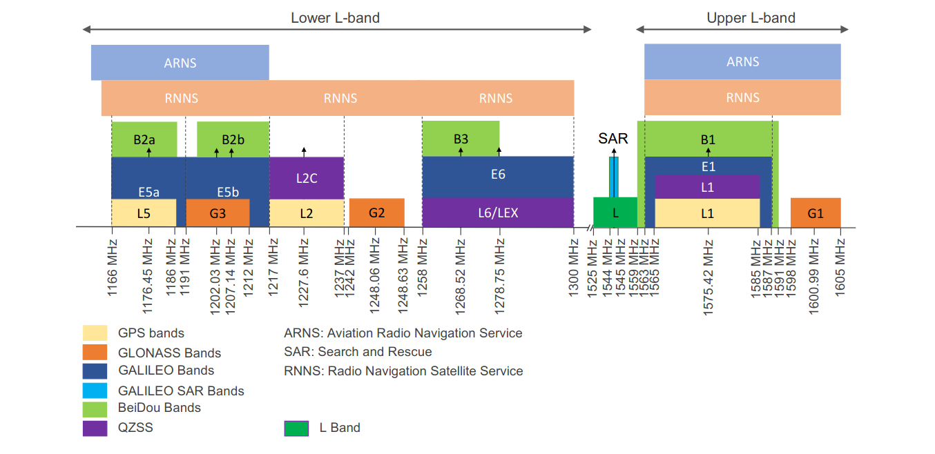
The grayed out area is the GNSS L1 band, which is the frequency range where the most popular GNSS systems operate. The image below shows the GNSS upper and lower bands with the L1 band to the right.
![]()
GNSS bands. Courtesy of farnell.com. We’ve also calculated the matching network components values using
MegiQ VNAsoftware, but since I’m quite pleased with the antenna characteristics, I’ve decided not to populate them and leave the 0 Ohm resistors in place.GNSS Module performance
Using GNSS module, the Time-to-first-fix upon cold-start was around 30 seconds under the open sky, which is close to the specified time in the datasheet.
![]()
SIM68M Typical Time-to-first-fix. The module was able to maintain a fix even in the middle of a room with no windows, which is quite impressive. Also, the module was able to get a fix when placed on a car seat, so they don’t need to be placed on the car dashboard, which is a plus in our case.
![]()
The moment I’ve managed to make a first GPS signal fix. Conclusion and Future considerations
Overall, I’m really satisfied with the GNSS circuitry design and implementation, however there are a couple of things I would like to improve in the future.
I want to replace
SIM68Mmodule with a cheaper one. Currently, the price of the module is around $7.5 per unit, which places it as the most expensive component on the board, and I’ve seen 2x cheaper modules with similar performance on the market.Also, I would like to experiment with different ground plane sizes to see how it affects the antenna performance. I would also like to try the smaller active antenna to see if we can reduce the board size.
Thank you for reading this post. If you have any questions or suggestions, feel free to leave a comment below. Stay tuned for more updates on the Catchcam project.
Note: If you’re interested, you can pre-order a sample at vnucec.ivan@gmail.com.
-
Writing and debugging first software
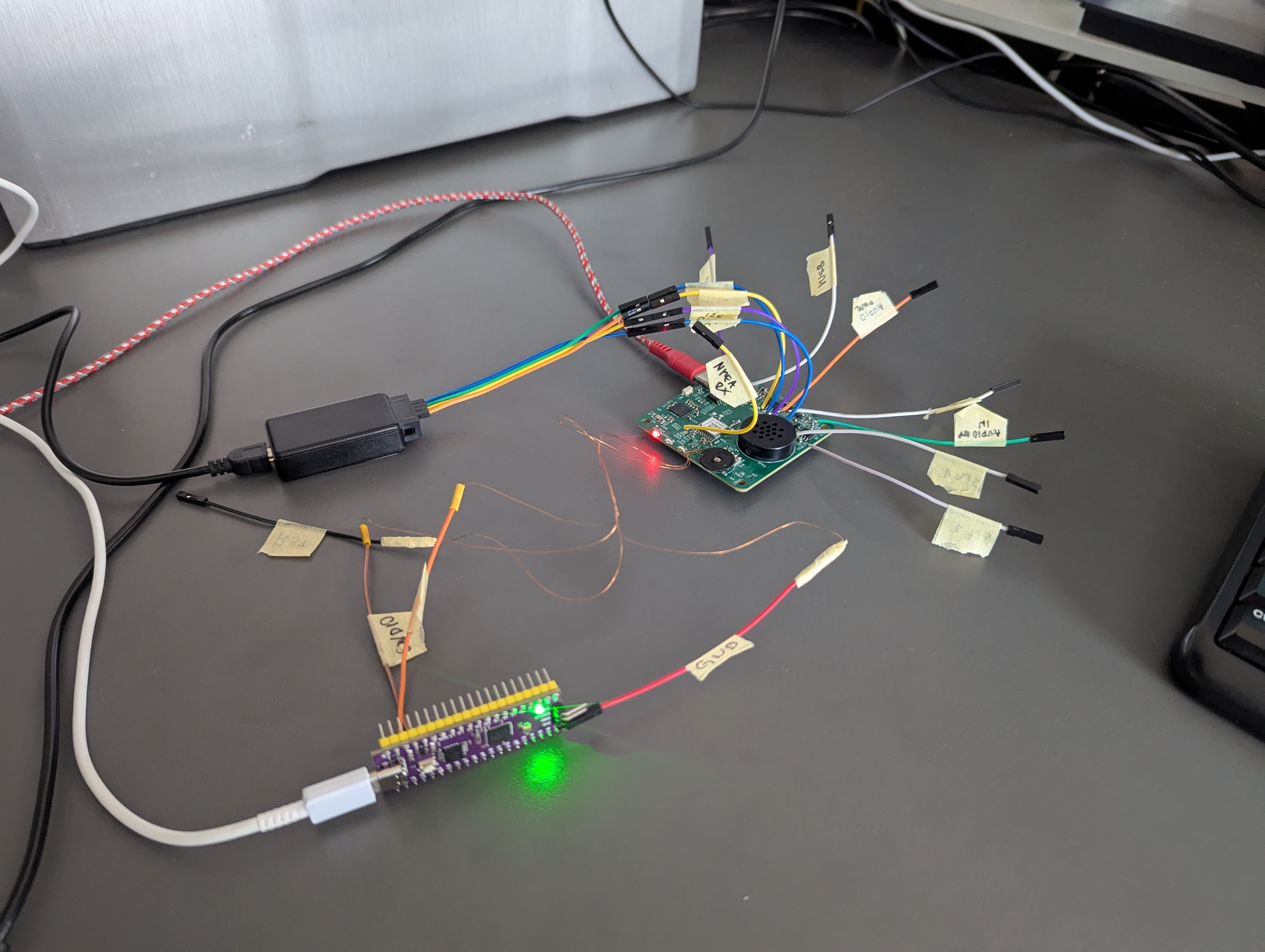
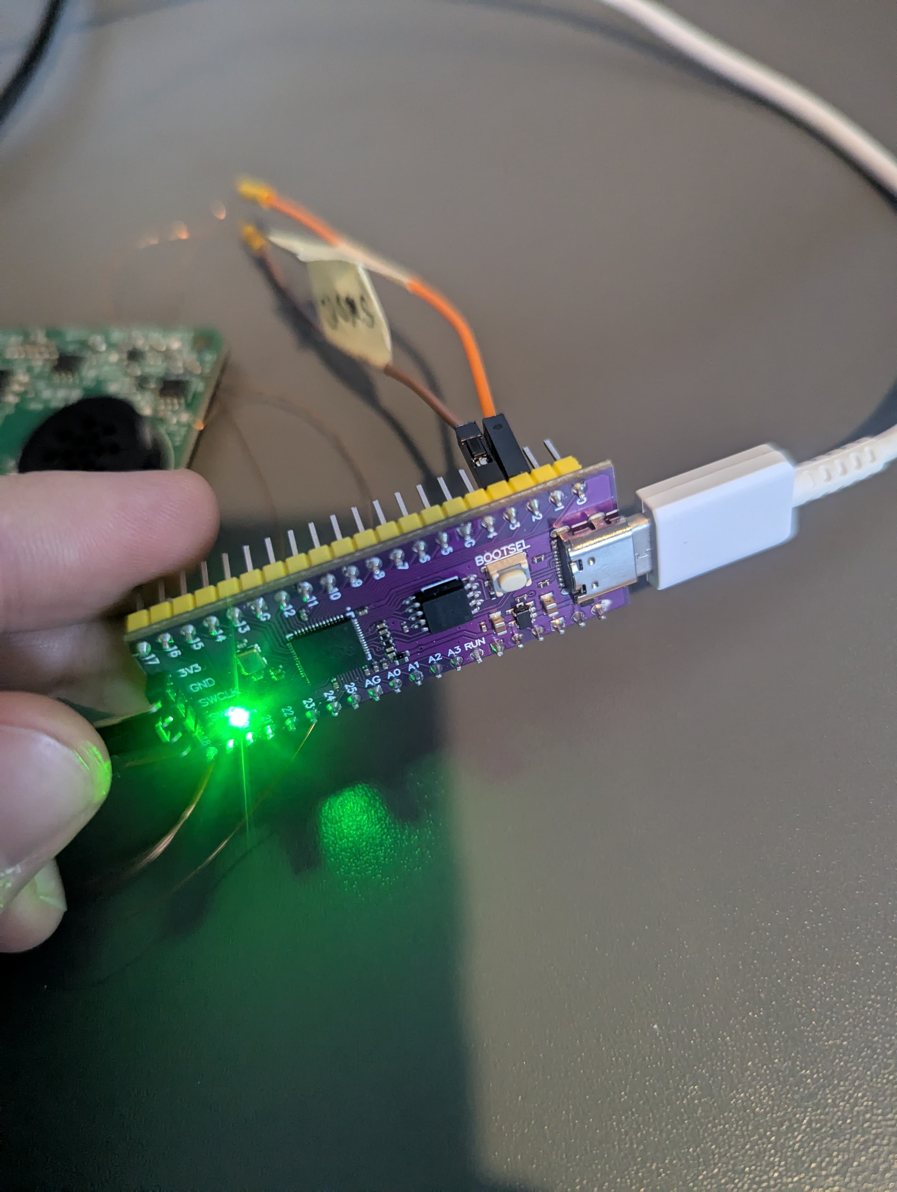
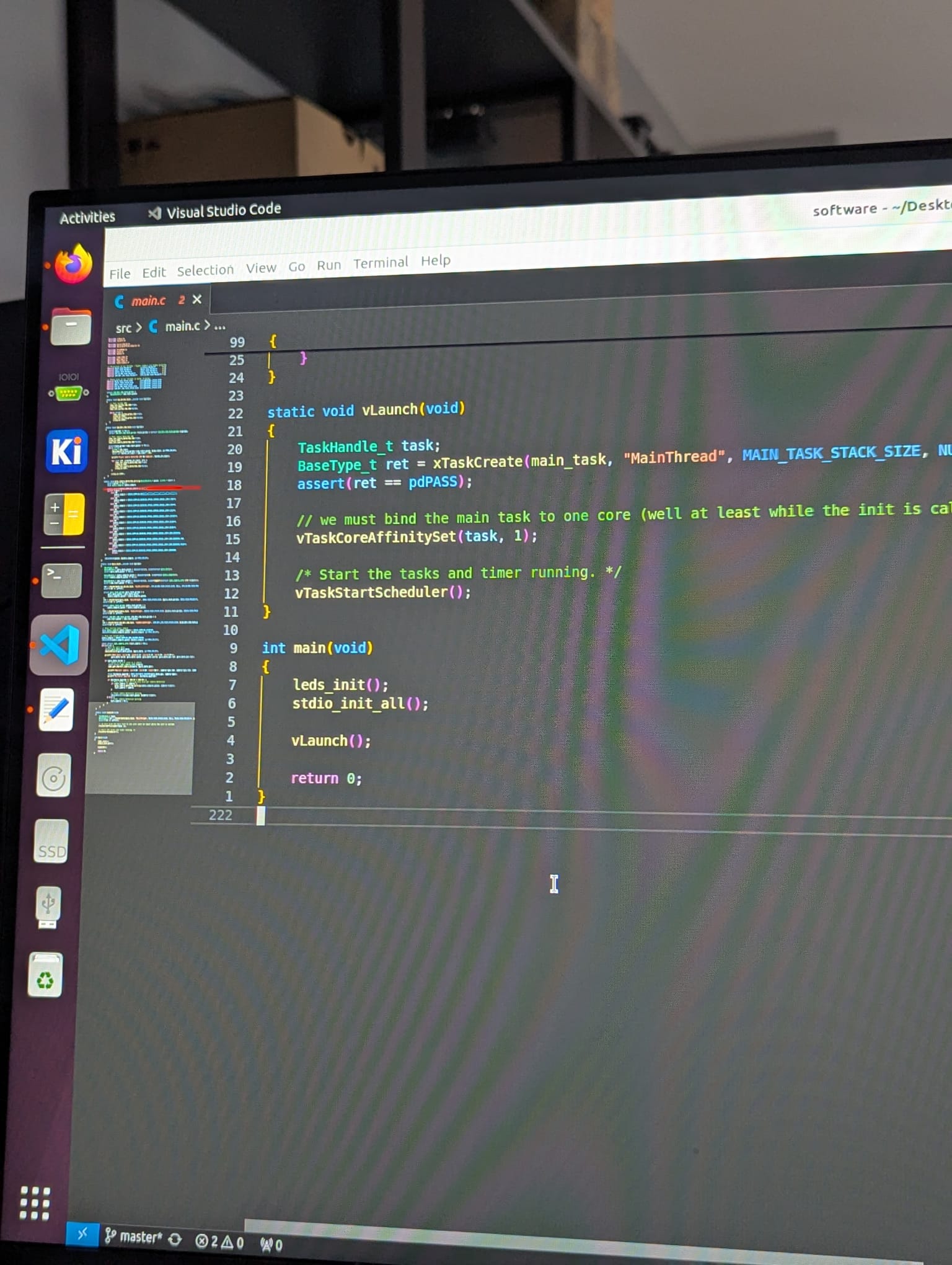
11/22/2024 at 08:19 • 0 commentsMaking progress on my #Catchcam project - a speed camera detector.
Just started writing the first software for it and now debugging using Raspberry Pi Pico and VS Code.
If you're interested in trying out a sample, send me an email at vnucec.ivan@gmail.com.
-
Boards have finally arrived
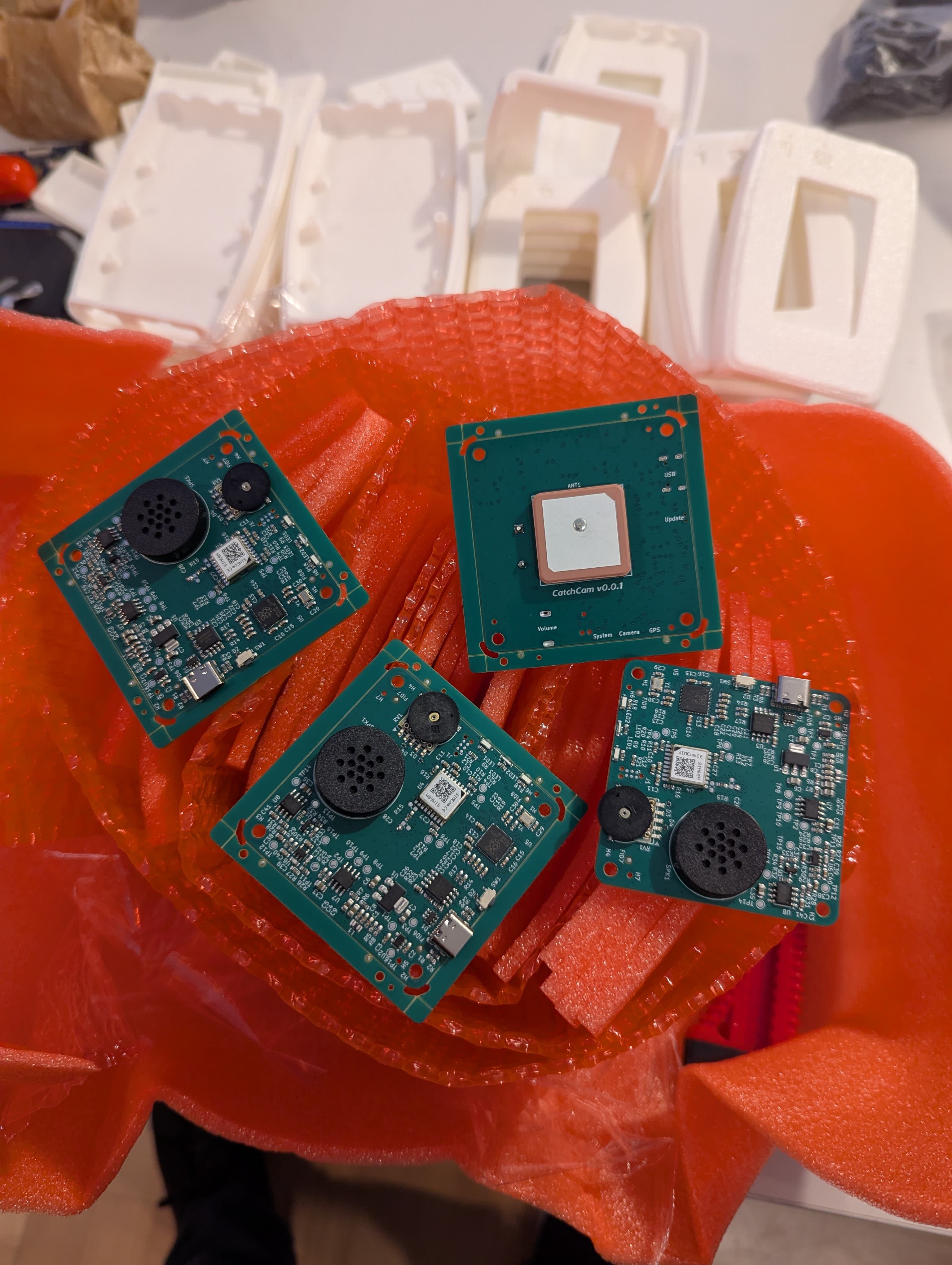
11/21/2024 at 15:02 • 0 commentsAfter weeks of waiting, Catchcam boards have finally arrived!
![]()
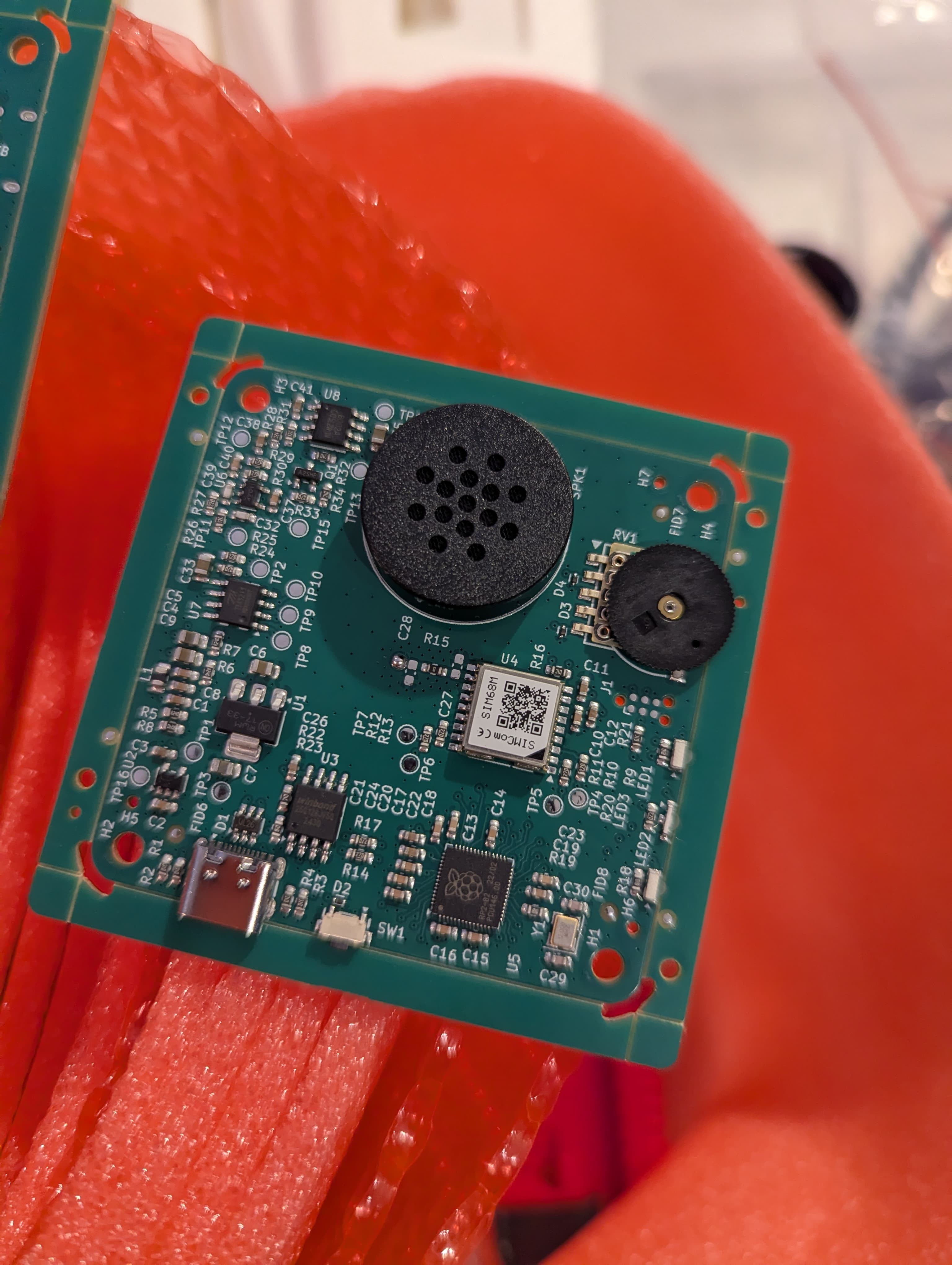
I've ordered 10 boards with components assembly included. The quality of the boards is exceptional.
The boards are quite clean and the components are well soldered.![]()
I've powered up the board, and tested the power supply voltages. They all seem fine.Next, I will try to flash and debug a simple program. Stay tuned!
(You can pre-order the Catchcam - Speed camera Detector sample at vnucec.ivan@gmail.com.) -
Designing Audio Circuitry
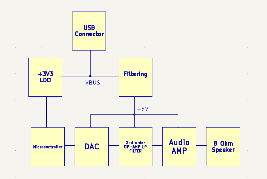
11/15/2024 at 14:07 • 0 commentsIn this post, I will be discussing the audio circuitry of the Catchcam. The audio circuitry is responsible for converting the digital audio data from the microcontroller into an analog signal that can be played through a speaker. Below is a block diagram of the audio circuitry of the Catchcam:
![]()
The audio circuitry consists of:
- power supply filtering,
- digital-to-analog converter (DAC),
- anti-aliasing (reconstruction) filter (AAF),
- audio amplifier, and
- speaker.Let's discuss each of these components in detail.
## Power Supply Filtering
When designing an audio power supply, it's important to ensure a clean and stable power source. In this case, the power supply needs to be at 5 volts and will be sourced from the USB connector (VBUS), which is connected to a vehicle's USB port.
However, vehicle USB ports can be a bit noisy, so we need to filter out this noise before it reaches the audio circuitry. A common approach that I've seen on the internet is to use a PI filter.
### Avoiding Ferrite Beads
Many PI filter designs online utilize a ferrite beads to prevent digital power rail ripple. However, I've read here and here that ferrite beads can actually amplify noise at certain frequencies and are not recommended for new designs, regardless of how popular they are.
Instead, I decided to use a `MLP2012H2R2MT0S1`, 2.2 μH inductor in a small 0805 package rated at 1 amps.
### Calculating the Capacitor Values
I spent a lot of time finding the right capacitance values, but on the same post above it was written: "Overall, if the filter performance is not critical, don't spend your time overanalyzing it". This have had me realized that the exact values of the capacitors doesn't matter that much, as long as they're in the right ballpark.
One thing to be careful about is the USB bus input capacitance because it is restricted by the USB specification to maximal 10 uF. However, I've placed more than 10 uF in parallel in order to increase the filtering. It can be done in my case because I have added an inrush current limiting IC connected to the VBUS line (see my older blog post about choosing components).
### The Final PI Filter Design
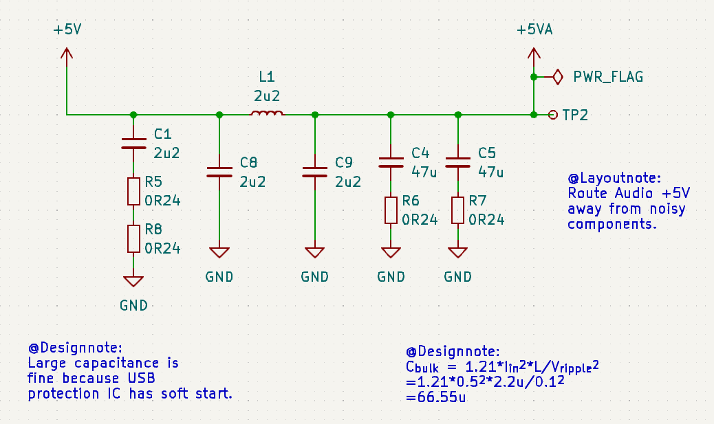
So, here is the PI filter I ended up with:
![]()
This filter should effectively remove the noise from the vehicle's USB port, providing a clean 5V power supply for the audio circuitry. I've also added a test point to measure the voltage ripple but I haven't measured it yet.
You may ask why there are multiple 0.24 Ohm series resistors? The series resistors provide additional damping and help with stability of the filter because ceramic capacitors have quite low ESR values compared to the Electrolytic caps. Why two 0.24 Ohm in series and not one 0.58 Ohm you might ask? Because I want to reduce bill of materials. You will see it in other parts of the schematic as well.
Here is a video from MicroType Engineering that I've found useful. It explains the design of the PI filter on a real world example. Also, this document from Texas Instruments explains the damping in more detail.
I also want to mention this blog post from Andy Brown, where he explains the USB filtering in more detail with beautiful oscilloscope graphs.
## Digital-to-Analog Converter (DAC)
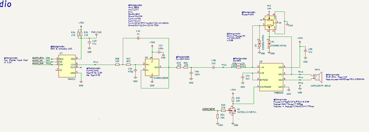
The DAC is responsible for converting the digital audio data from the microcontroller into an analog signal. I've chosen the `TM8211` DAC which is chinese version of `PT8211` DAC. It's a 16-bit two-channel DAC with I2S interface. Because it's R-2R type, the output voltage swing is from 0 to VDD/2 volts (as demonstrated here). So, in our case it's 2.5 volts. DAC sampling rate is set to 44.1 kHz, which is the standard audio sampling rate for CD-quality audio. The higher the sampling rate, the better the audio quality, but it also requires more memory (44.1 samples per second of audio) to store the audio data. We are using only one channel of the DAC because we have only one speaker.
I would like to mention this video from Sandrine Sims, where she had created a fun project using the PT8211 DAC. Also, this video from Gadget Reboot nicely explains the PT8211 DAC and compares it to the direct MP3 output, and `UDA1334A` DAC.
## Anti-Aliasing Filter (AAF)
The AAF is a low-pass filter that removes frequencies above the Nyquist frequency (half the sampling rate) to prevent aliasing, and also to provide low impedance output because DAC output value could change based on the output load that it is connected. In our case, it is the input of the opamp which has theoretically infinite impedance. I've chosen a 2nd order Sallen-Key low-pass filter topology referenced here. The filter is implemented using `TLV9061IDBVR` single-rail opamp. The filter components are chosen based on the following calculator. The filter is designed to have a gain of 1, with a cutoff frequency at about 22.05 kHz (half of DAC the sampling rate frequency).
You can see that I've added another low-pass filter at the opamp output in order to further eliminate the high frequency noise introduced by the non-ideal opamp characteristic as mentioned here.
## Audio Amplifier
The audio amplifier is responsible for amplifying the analog audio signal to a level that can drive the speaker. I've chosen the `FM8002A` chinese audio amplifier. I've choosen it after watching this video from LeftyMaker, which shows that you can reproduce quite nice audio with this cheap amplifier.
In our design, the amplifier gain can be set using a 10 KOhm `RK10J12R0A0B` rotary knob, which is useful for adjusting the volume. Maximum gain is set to 3.08 (see math on the scheme) in order to avoid exceding the speaker's power rating.
Also, the amplifier has a shutdown pin which can be controlled by the microcontroller in order to further eliminate a hum noise when the speaker is not in use. The amplifier datasheet doesn't specify the input pin voltage so the pin is driven by a n-channel MOSFET.
## Speaker
I've chosen a `GSPK2307P-8R1W` speaker with a power rating of 1 watt. The speaker is directly connected to the audio amplifier outputs. I haven't looked into the speaker's audio waveform yet, but I'll add it to this post later.
## Conclusion
In this post, I discussed the audio circuitry of the Catchcam. The audio circuitry consists of a power supply filter, digital-to-analog converter (DAC), anti-aliasing filter (AAF), audio amplifier, and speaker. I've chosen the components for each part of the audio circuitry based on their performance, cost, and availability. I'll add measurements and audio waveforms to this post later.
Here is the final schematic of the audio circuitry:
![]()
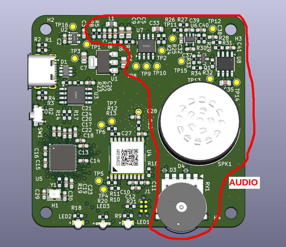
And here is the final PCB layout of the audio circuitry:
![]()
Stay tuned for more updates on the Catchcam project!
Also, if you're interested, you can pre-order a sample at vnucec.ivan@gmail.com.
-
Choosing Components
11/12/2024 at 09:15 • 0 commentsIntroduction
Lets choose major hardware components for the Catchcam project. As I've written [before](https://ivanvnucec.github.io/tags/#catchcam), the idea is to have a plug and play device that alerts if the vehicle is approaching a speed camera both via sound and LED signal.
Catchcam draws power from built in USB-C socket that is connected to a vehicle USB socket. As for the user interfaces, it has a small speaker, a volume potentiometer, System status LED, GPS signal status LED, Camera alert LED, and a Software update button (more on that later). In order to know the current position, Catchcam has GNSS module with an on-board Antenna. Moreover, to reproduce audio alerts, Catchcam incorporates DAC, Low-pass anti aliasing/reconstruction filter, and an Audio amplifier.
Lets go through the components one by one.
Components
Microcontroller and Flash
First we will choose the microcontroller. Initially, I was thinking about choosing one of the STM32F microcontrollers such as STM32F407 for example, with the hardware FPU, but the prices are astronomical, and in my opinion, there are better and cheaper alternatives. Futhermore, the STM onboard Flash memory is around 1MB max., which might be too low for us in order to store more than all the camera positions along with audio samples. In order to incorporate all of that, I would certainly need additional external flash which would increase the cost and complexity of the design.
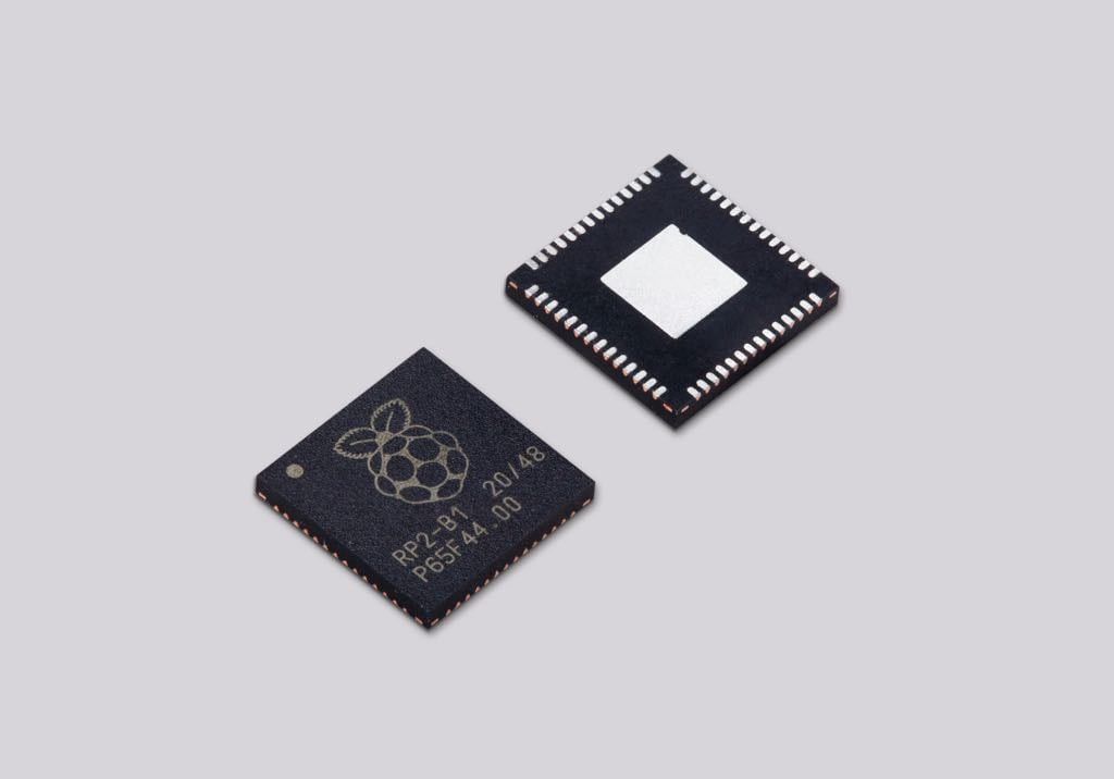
The decision has been made on the popular [rp2040](https://www.raspberrypi.com/products/rp2040/specifications/) microcontroller from Raspberry Pi Ltd. I've really liked this option because it features flexible I/O with dual-core Arm Cortex-M0+ processor, 264 on-chip SRAM, and best of all - Drag-and-drop programming using mass storage over USB. I love the idea that you can simply update the software by just drag-and-dropping already built firmware, which is ideal for project because an ease of updating camera positions is a must! You don't need any external hardware or software to update, nor you need any special computer knowledge. It's as simple as using an USB drive stick.
![]()
The software resides on the `W25Q128JVSIQ` external 16MB flash chip, which is a plenty of storage for all the camera positions and audio samples (which populates most of the flash) along the software.
![]()
GNSS Module and Antenna
The second major part of the project is a GNSS module. I've searched for a low cost solution and stumbled on the `SIM68M` module from SIMCom Wireless Solutions Co.,Ltd. I've also seen u-blox ones, but I havent taken them into consideration because I've had good experiences with the SIMCom modules in the past. SIM68M features an in-built LNA amplifier with support for the active GNSS antenna. Futhermore, SIM68M supports all of the major GNSS satellite constellations so the device can work across the globe.
![]()
The second important factor is the GNSS antenna. I've spent great deal of time searching one. The idea is that the Catchcam would reside on the vehicle's dashboard with the clear view of the sky in order to achieve best signal reception.
There are several antenna options to choose. There are two major divisions of the GNSS antenna types: active and passive. The difference is that the active antenna has build in LNA amplifier with the SAW filter in order to amplify and filter signal. Passive antennas lack those features. In the high-noise/low-signal scenarios, the active antenna is recommended. In my case, with the clear wive of the sky, and with the GNSS module build-in LNA amplifier, I've chosen the passive antenna type. Moreover, I've heard that there might be a problem if you use both the active antenna and in-built LNA because there might be an over-saturation of the signal, but I'm unsure of the claims because GNSS signal is rather weak anyway.
Besides active and passive ones, GNSS antennas comes in different packages and I will name a few. There are PCB Patch antennas, Ceramic Chip antennas, Ceramic Patch antennas, and Helix antennas. Helix antennas have good signal reception regardless of its orientation, and it is popular in a hand-held devices. However, Helix antennas are rather small in size, and the size is an important factor. The larger the antenna, the more signal amplification it has (with respect to the dipole antenna). Ceramic chip antennas are compact solution for mobile devices but they are too rather small. PCB patch antennas are good choice because you don't need to incorporate another part, however I'm not sure how good they are in terms of signal amplification.
As Catchcam is not hand-held, nor particularly small, I've chosen to go with the `KH-GPS252504-WY` Ceramic Patch antenna. It's 25x25 mm in size, and it has a good signal reception. However, it needs to have large ground plane (about 50x50 mm is fine) in order to work properly.
![]()
Audio
Speaker
The next comes the speaker with it's owm audio reproduction circuitry. I would like to power the speaker from the USB 5V VBUS. With the 500 mA VBUS current limit (defined by the USB standard), we can theoretically have max. power of 2.5W (5V * 500 mA), so 1W speaker might be enough in our case. I'm unsure about sound level at 1W, but we'll see. I'm afraid that the user might miss the camera alert if they are listening to loud music for example.
There are variety of speakers out there: from the physically large ones with good audio spectrum characteristic especially in the low frequencies bass tones, all the way to the small Trough-hole or SMD speakers. With the regards to the smaller ones, there are ones with the external power leads so you can mount them directly to the enclosure, and there are trough-hole/SMD ones that can be soldered directly to the board.
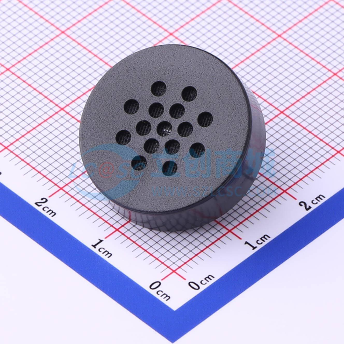
I've chosen the `GSPK2307P-8R1W` trough-hole, 1W, 8 Ohm, 88 dB speaker. It's 23 mm in diameter and 6.8 mm in height. I've also considered the SMD ones but they are rather expensive compared to the trough-hole ones.
![]()
Audio Amplifier
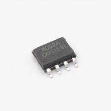
The speaker is driven by the Audio amplifier that is powered by the filtered VBUS voltage. I've stumbled on the popular and design-proven `LM358` but I have dropped the idea because the signal input has to be biased. Being intrigued by [Did I make the cheapest DIY amplifier?]() video that references cheap chinese `FM8002A` audio amplifier, I've chosen it for audio amplifier. It can deliver 1.5W power to the 8 Ohm load, handle 5V power supply, the input signal doesn't need to be biased, and it has adjustable gain which enables volume control. It also features a Shutdown mode which mutes the output which I like because I'm afraid that the noise could creep onto a signal trough the USB car connection.
![]()
DAC and Reconstruction filter
The audio amplifier input signal is generated with 12-bit `TM8211` DAC and Low-pass Anti-aliasing/reconstruction filter (Sallen-Key topology). TM8211 is cheap chinese `PT8211` knockoff. The data from the microcontroller comes over I2S bus to the DAC, which is referenced to the filtered 5V VBUS. That all results in a 0.0-2.5 V signal swing at the DAC output.
![]()
Audio samples are sampled with 44.1kHz frequency rate. Signal from the DAC output is then reconstructed with the active Low-pass filter with a cut-off frequency set to about half of the sampling frequency. For the active filter, I've chosen `TLV9061IDBVR` OP-AMP because it is a rail-to rail amplifier that can be powered with the 5V. Gain of the Low-pass filter is set to 1. I will write about signal generation and filtering in another post.
![]()
I've also incorporated `RK10J12R0A0B` knob type potentiometer so the user can set the audio volume. The potentiometer resistance directly affects the audio amplifier gain so the signal to the speaker can be reduced all the way to the zero.
![]()
User Interfaces
USB-C Connector
As for the USB connector, I've chosen standard USB-C (USB v2.0) SMD connector at a 90 degree angle. Also, I've added the `NCP361SNT1G` USB Over-voltage and Over-current protection IC, and added the `USBLC6-2SC6Y` ESD protection to protect the VBUS and data lines from static discharges.
LEDs
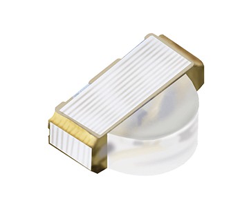
Both the System status LED and GNSS Signal status LED, I've chosen `12-22SURSYGC/S530-A2/TR8` 90 degree angle SMD led that encapsulates both Green and Red LED in the same package. The idea is that the System status green color LED blinks periodically, and if some error happens, it becomes red.
Similarly, the GNSS signal status stays green as long as the GNSS data is valid, and if signal is lost, it becomes red. As for the Camera detected LED, I've chosen `TJ-S3210SW5TGLC6B-A5`. It's also 90 degree angle SMD LED but with a blue color. The driving current for the Camera detected LED is somewhat higher at 10 mA in order to be visible even under daylight sun.
![]()
Software Update Button
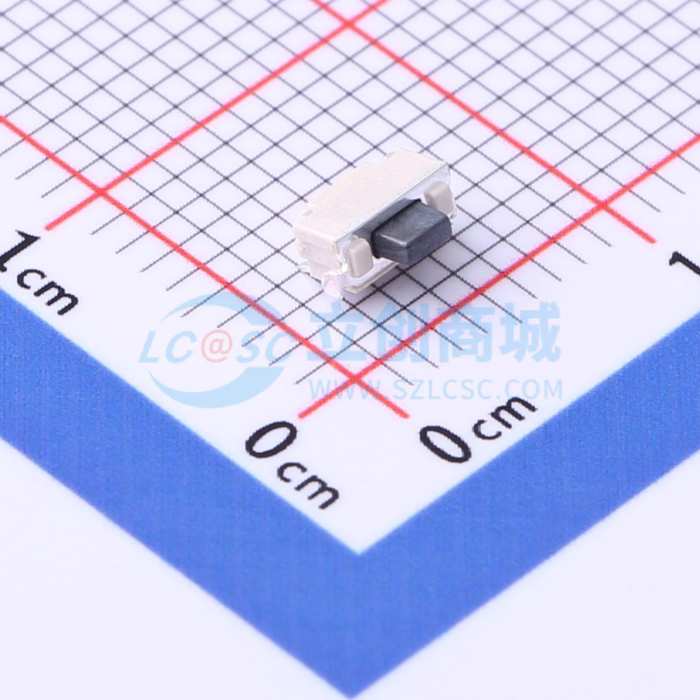
And lastly, there is a small `TSA002A3518B` 90 degree angle push-button that enables software updates. The idea is that the user can easily update its device firmware by connecting it to a PC and simply drag-and-drop the new firmware. In order to do that, the button needs to be pressed while the user connects USB cable to a PC. This would then trigger the in-built rp2040 USB mass storage bootloader which would then present the microcontroller storage as a USB mass storage media device and enable firmware drag-and-drop feature.
![]()
Power Supply
The 5V comes from the USB connector to the `NCP1117ST33T3G` 3.3V, 1A fixed voltage linear regulator. The 3.3V is then distributed to the microcontroller, and GNSS module. The 5V is then filtered with the simple CLC (PI) filter and then distributed to the DAC, Low-Pass filter, and finally to the audio amplifier. Audio filtering will be discussed in another post.
![]()
ConclusionAnd that is basically it when it comes to the components. We're left with the passive components that will not be discussed.
Future considerations
I've thought a lot about incorporating so the device can be mounted on a vehicles that are lacking USB ports such as old vehicles or motorcycles, but I've dropped the idea for now because I don't want to drop design simplicity in the project prototype phase. I've also been thinking about incorporating GSM module so the devices can automatically update its software, but that was also dropped because of the complexities involving a server that would enable those updates. Also I would need to have SIM cards that works across the globe, and with different internet providers... Just not worth it for now.
Also, if you're interested, you can pre-order a sample at vnucec.ivan@gmail.com.
Catchcam - Speed Camera Detector
Offline speed camera detector designed for a hassle-free driving experience, while respecting your privacy.
 Ivan Vnucec