Retro rack and backplane computer
Old style modular system for development of retro computers
Old style modular system for development of retro computers
To make the experience fit your profile, pick a username and tell us what interests you.
We found and based on your interests.
I have been arguing with printers all day trying to print the next version of the back plane -
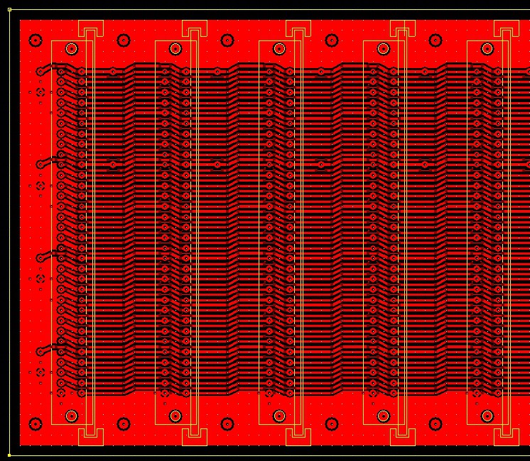
I discovered that there was problems with the printing more so than the board.
I used an older printed PCB as a reference and I discovered that the 10 mill traces were coming out at 5 mill on the printer.
So instead of WYSIWYG it's more like WYSINWYFG!
After arguing with printer setting for a couple of hours, I gave up and change the size of the traces.
Even then I had to shorten the board as something in the computer (that I can't find - and I was once a CME) is setting the paper size to LETTER instead of A4.
The traces are now 20 and 30 mill and shrink to 10 and 20 mill between pads.
I also dropped the unused middle row of pins in the connectors to give a little more clearance.
It's too late in the day now to go cutting laminate and playing with chemicals so I will get back to this tomorrow some time.
I also got some countersunk rivnuts and they don't work so well without the rivnut tool. The M3 screws strip. I will buy a rivnut tool and that will solve the problem.
I have more or less decided on the Euro Card standard of 160mm x 100mm as I can get that size in my country and I don't need to cut them. The Chinese boards (150mm x 100m) aren't even square and their too thin.
UPDATE!
Well, I did another etch.
I dropped the laminate during toner transfer ans caused some breaks -
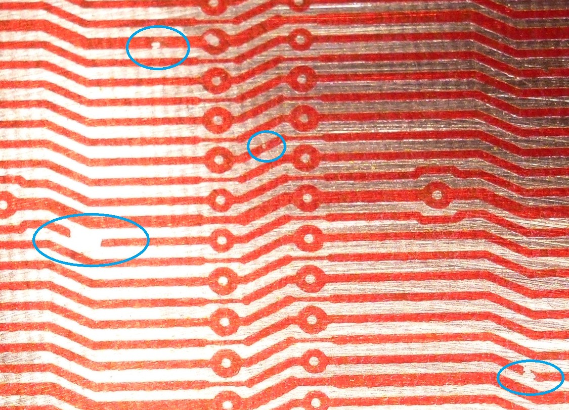
I decided to ignore them and continue as I can fix them with bits of wire and solder. I can *actually* see the traces now. Normally I have to use a Digital camera and zoom it on mt 37" monitor as I have *old* sight now lol.
The Toner Reactive Foil (TRF) creased as it went through the laminator, leaving some gaps due to the creases. It's much easier to examine the green TRF if I use Red toner. This is not critical as the traces are large enough that it *should* work without TRF just how others do plain toner transfer.

I re-did the TRF anyway and you can see from the peeled off sheet that it filled the gaps -

I tried tinning the old board to see how it goes and I decided against it and just used the normal PCB protective coating -
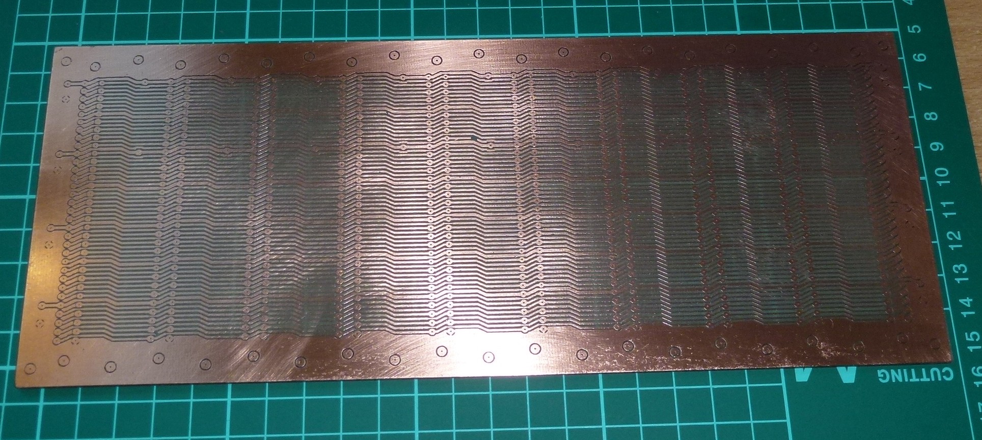
There are 10 x 64 pin sockets so I have at least 640 holes to drill and a bit of patching up a small number of broken tracks.
I am going to try to use strip board as a guide to drill the holes. I will test on the old board first.
By the way, the real small traces ( <5 mill) on the old board were fine! It was just under etched on the sides. I prefer this version anyway because I can *just* see the traces with natural vision.
I will hopefully drill the holes tomorrow. It may be a busy day tomorrow so I will see if I can find the time.
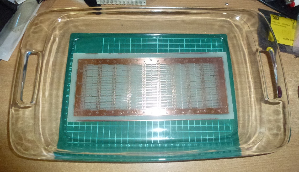
Well, I haven't made another back-plane yet but at least I have an etch bowl that will fit it. This bowl comes very close to fitting an A4 piece of paper to anything I can print, I can also etch. I don't want to waste connectors on the poor quality one that didn't come out right.
There were a number of issues, one of which related to printers. I have several printers here and I am not sure which one was best for toner transfer.
I have an old HP 1300 mono LASER which is great for banging out PDFs. When I tried that there seemed to be an error in scaling. I don't know if I have used it for toner transfer before, probably not. I have another mono LASER (Canon LBP3000) and it is in storage. I seem to recall that it started having paper pickup issues (probably needs a paper separator). I think it may have been the better printer for toner transfer. Both of these mono LASERs need direct USB connection.
In a hallway cupboard I have the color LASER that I used recently. It's Wi-Fi. I have used it before and I remember there being imperfections in the resulting board due to what looks like issues with the transfer belt.
Just today I went to buy 4 privately sold toner cartridges for the color LASER. The seller also had 4 partially used cartridges as well (they're about 3/4 full).
When I went to pick them up he mentioned the history of the cartridges. Her had a color LASER and it developed paper pickup issues when new so he just put it back in the box and stored it and then went an bough another the same. The second unit went for a reasonable time and has an issue with the toner density setting - it's grubby in there - toner around and that will be *the* issue.
He gave both of the printers to me as he going to through them out anyway.
As you can guess the one mentioned about probably just needs a clean out.
I the tried the other one that had been stored when new. It has an intermittent paper pickup issue. I have almost diagnosed the problem. It lifts the paper to the pickup roller. I suspect the paper lift is not dropping down sometimes and causing the next sheet to feed too early. Such an easy problem to solve, if that is the case.
I did a test print and it's absolutely perfect !!!! I am so happy about that.
The only real problem now is that it is also USB and I can't two printers near the computer so perhaps I will just have to forgo the mono LASERs for now.
As an added bonus (hopefully) the parts from the smaller color LASER printer that is left over can be used to fix the larger network color multi-function printer which needs a transfer belt and fuser film sleeve.
Also today, I found a much larger Pyrex etching bowl that will fit larger boards. I bought some 150 x 150mm double sided PCB because that's largest double sided I can buy around here. I was thinking of doing 150mm lengths of back-plane that plug together. Just a thought though. I really do want to have double sided and leave one side un-etched as a ground plane. Perhaps is time for another long distance order.
Now I am thinking of a small dedicated print server so I can put all 5 printers in one place.
Anyway, I have some work to do to get a printer setup that I am happy with. I really don't want to leave myself with ONLY color LASERS as the toner gets expensive. My HP 1300 mono LASER is only 8 cents per sheet, it's a shame it has a scaling issue, probably scaling my A4 prints to what it believes is 'Letter' there is no software available to change this setting that works on my OS. The other mono LASER is even cheaper with non-genuine toner but it's poorer quality as well.
On a side note -
My network connection broke when I was typing this so I saved the text and rebooted the computer and that is why everything seems double spaced - big gaps between paragraphs.
Windows uses [CRLF] as line ending, *nix uses [LF] and mac uses [CR].
so the fix for anyone who ever coded on a web server is -
$text = str_replace("\r\n", "\r", $text);
$text = str_replace("\r", "\n", $text);
on *nix...
Read more »Well here is what went wrong (in pictures) -
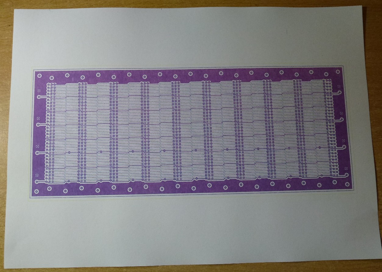
Above: Plain printout using color LASER printer.
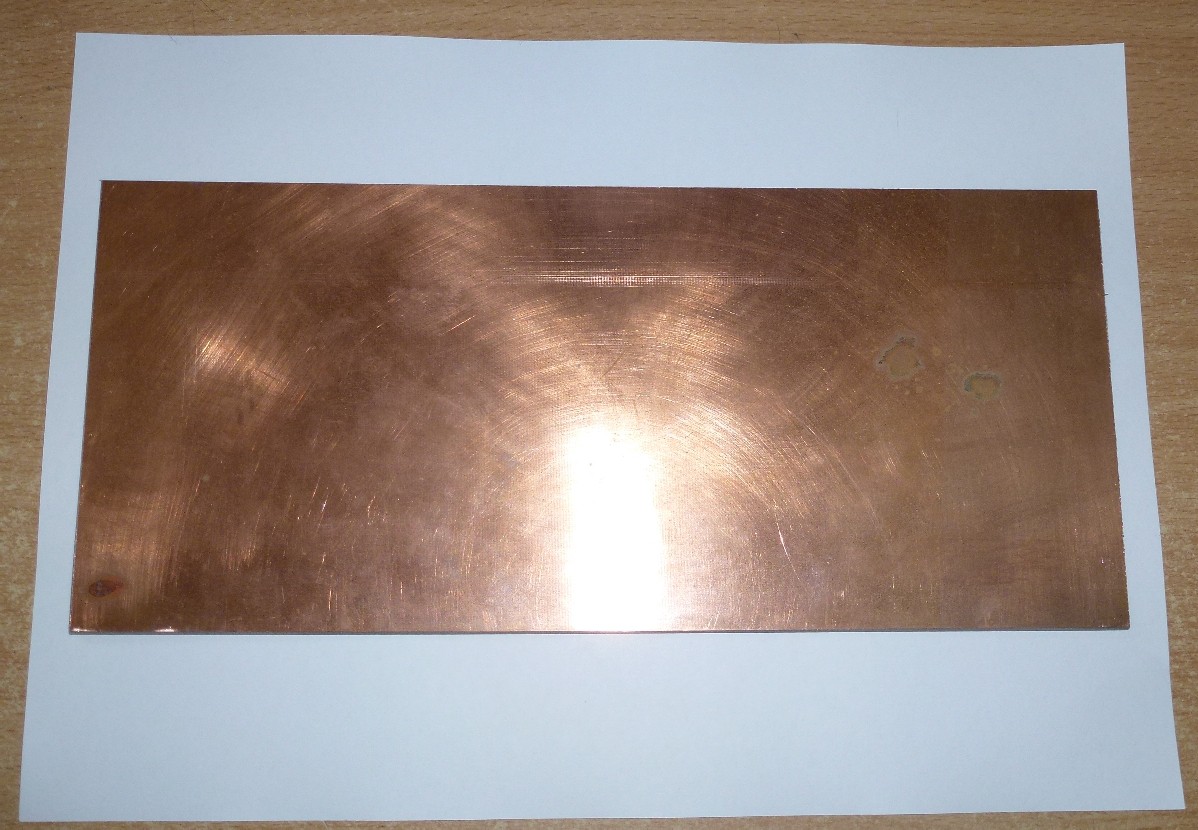
Above: Dirty FR4 roughly cut to oversize.
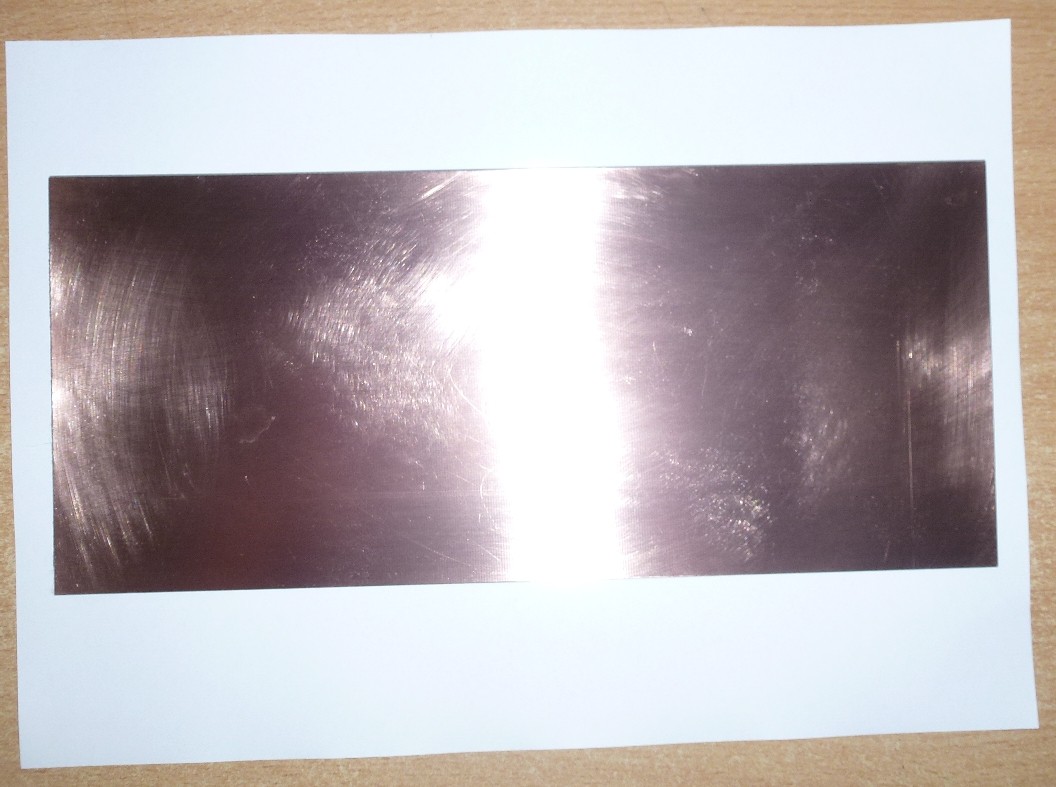
Above: Cleaned
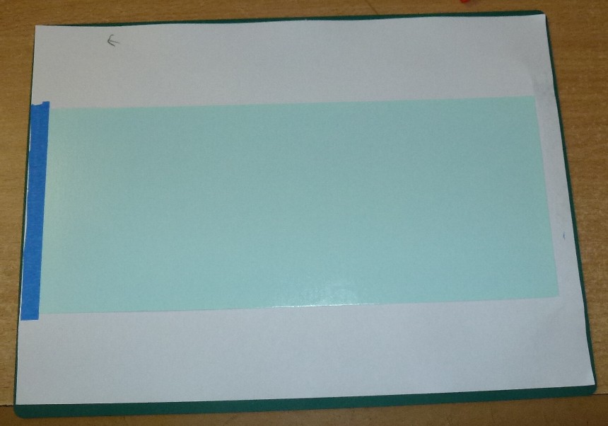
Above: Dextrin sheet made by Pulsar - This is the *good* sauce, you get 100% toner transfer every time
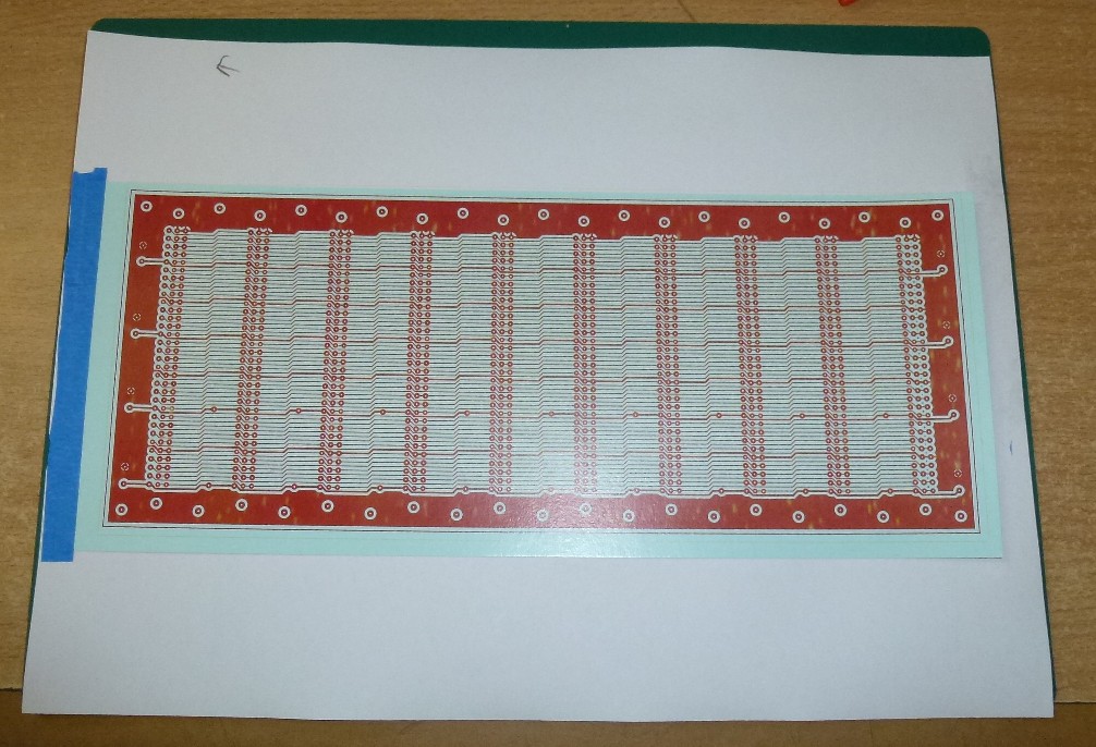
Above: Dextrin that has been printed on
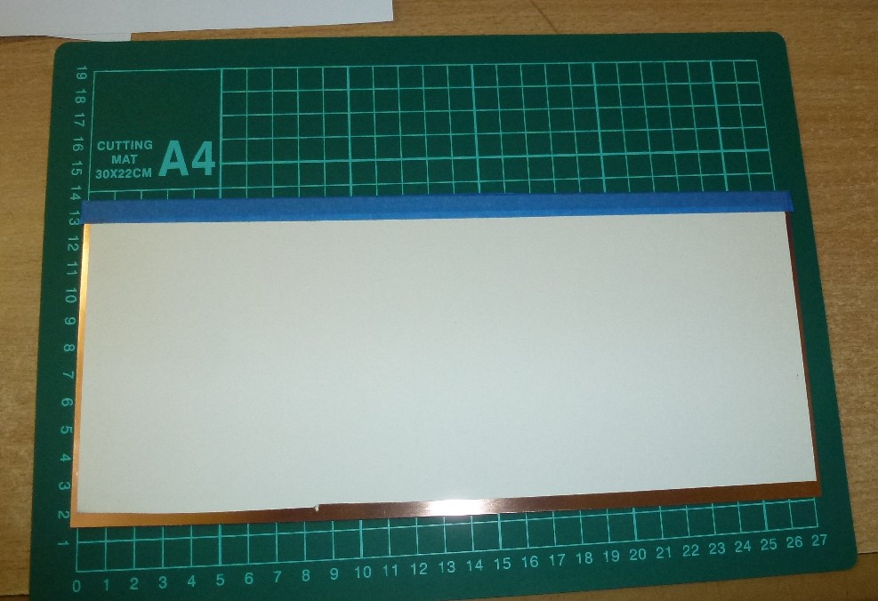
Above: Dextrin taped to leading edge of board for fusing
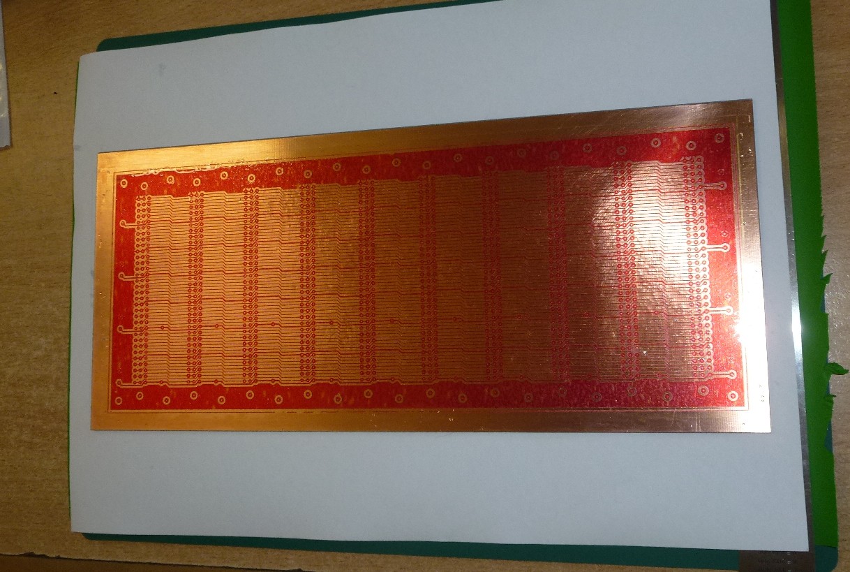
Above:Toner fused to FR4 by laminator
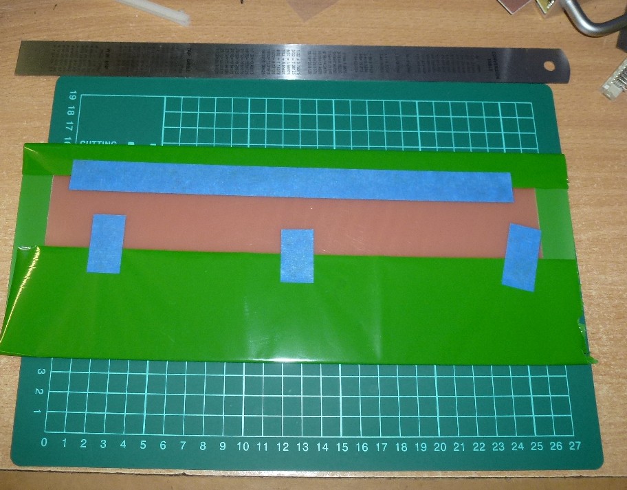
Above: Toner Reactive Foil (Green TRF). The is the *secret* sauce. It will get you down to 5 mil traces when you get the other things right as well.
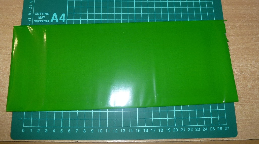
Above: TRF ready for fusing with laminator
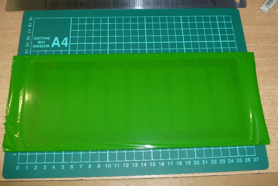
Above: You can see the traces fused.
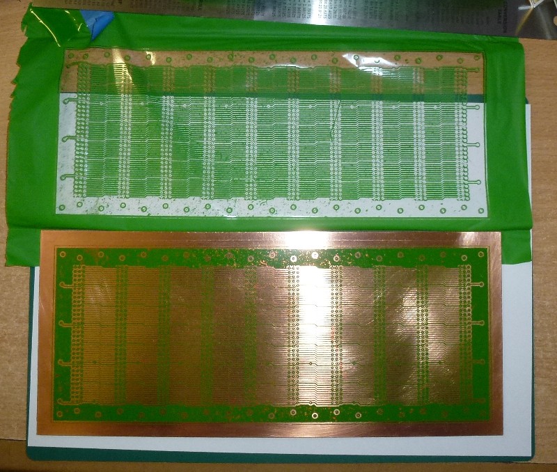
Above: I missed it! The green diagonal line on the fourth socket position from the right that you can see on the Toner Reactive Foil. Explained later.
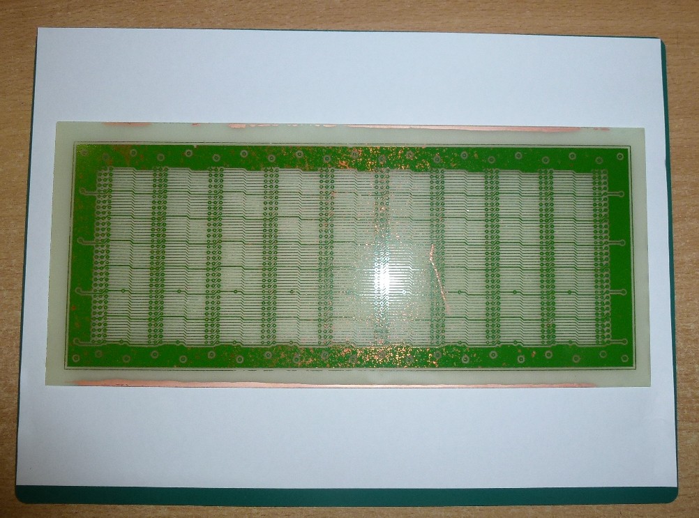
Above: I missed it again, that same line after etching.
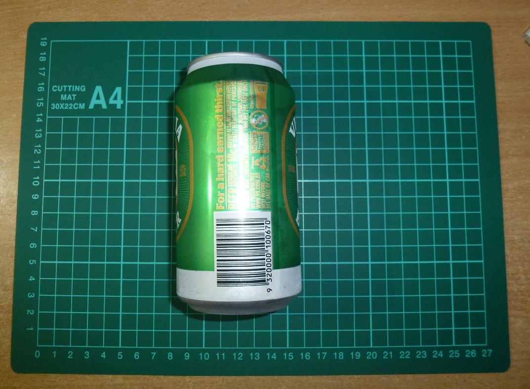
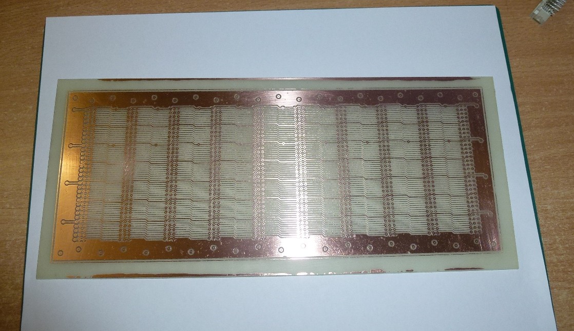
Ok, The problem wasn't the beer lol. I am drinking that now - not when I was doing the board.
A number of things went wrong and here they are -
1) I used 10 mill traces when there was room for 15 mill traces. I wanted to fix this in the CAD but there was no way to edit trace widths except for one segment of one trace at a time. This shouldn't have been a problem BUT it added to other issues. I have made PCB this way down to 7 mill traces.
2) The diagonal line mentioned in the pictures above was a clue that I missed. The printer I used has a tear in the fuser film sleeve and that more or less destroyed the quality of the end product.
3) This board won't fit into my etch bowl. I left it elevated at on end and used a brush to brush on the etch. This really doesn't work for the etch I use as it needs to be kept at 70 C which doesn't happen when one end of the board is in free air. As a result the board is over etched in the middle and under etched on the ends.
I didn't have a good look at the board yet but it's probably unusable. I will have to come up with a plan 'B' or try to find a lager etch bowl or make the board in two halves. And either fix that printer or try or buy another.
Anyway, I will worry about that another day.
I've started laying out the back plane -
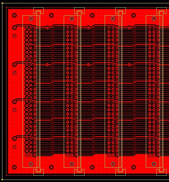
I am having some issues. The backplane is bigger than a A4 sheet of paper so I have been cutting the width of it back. It is still printing out of proportion and I don't know why. What should be 11 inches is coming out as 10.9 inches on paper.
After this issue occurred I went and checked my etching bowl and it's too small as well :(
The connectors arrived, 5 of each. Enough to get started.
The layout is like this -
Power
8 signals
GND
8 signals
Power
8 signals
GND
8 Signals
Power
8 signals
GND
8 Signals
Power
8 signals
GND
Signal level compatibility tests -
XC9536XL CPLD   NMOS Z80  Noise Margin
Low  Out 0.4V < 0.8V      0.4V
High Out 2.4V > 2.0V      0.4V
Low  In  0.8V > 0.4V      0.4V
High In  2.0V < 2.4V      0.4V


XC9536XL CPLD   CMOS Z80  Noise Margin
Low  Out 0.4V < 0.8V      0.4V
High Out 2.4V > 2.2V      0.2V
Low  In  0.8V > 0.4V      0.4V
High In  2.0V < 2.4V      0.4V


Z80  CPU (NMOS) Max 8 MHz
Vil = < 0.8V
Vih = > 2.0V
Vol = > 0.4V
Voh = > 2.4V
Iol = 2mA
Ioh = -250uA
Ii  = 10uA


Z80 CPU (CMOS) Max 20 MHz
Vil = < 0.8V
Vih = > 2.2V
Vol = < 0.4V
Voh = > 2.4V
Iol = 2mA
Ioh = -1.6mA
Ii  = 10uA


XC9536XL CPLD Vio = 3v3
Vcc = 3.0V - 3.6V
Vol = < 0.4V
Voh = > 2.4V
Vil = < 0.8V
Vih = > 2.0V
Iol =  8mA
Ioh = -4mA
Ii  = 10uA
Conclusion -
These chips are compatible. The weakest point is a high from the CPLD to the CMOS Z80 where the noise margin is only 0.2V
I have two plan 'B's for this issue -
1) I have both 3v3 and 3v6 LDO voltage regulaors in the same package so that if I have trouble with the CMOS CPU then I can run the CPLD with a 3v6 Vio to lift the Voh a little to improve noise margin.
2) I will ZIF socket the CMOS CPU so that as a last resort I can remove it and replace it with a NMOS CPU
As the signals between the CPLD and CPU will be short (on one card), I am not really expecting that the 0.2V margin will be a problem.
Perhaps as a third backup I could design in a regulator on the CPU board to provide the 5V Vcc from the 12V rail so there are no issues with the Vcc being a bit low after coming from teh backplane. The CPLD will already have onboard regulation.
Short glossary of terms -
Vo - Voltage output
Vi - Voltage input
h - high
l - low
Io - current output
Ii - current input offset
Vio - IO voltage for CPLD
Vcc - chip supply voltage
Here is a draft bus layout -
 1 +5V   +5V
 2 +12V  +3.3V
 3
 4
 5
 6 } 18 pins for other signals
 7
 8
 9
10
11
12 REFSH RESET
13 M1    CLK
14 INT   NMI
15 BUSRQ BUSAK
16 HALT  WAIT
17 MREQ  IORQ
18 RD    WR
19 A14   A15
20 A12   A13
21 A10   A11
22 A8    A9
23 A6    A7
24 A4    A5
25 A2    A3
26 A0    A1
27 D6    D7
28 D4    D5
29 D2    D3
30 D0    D1
31 GND   GND
32 GND   GND
----------------------
64 Pins Total
56 Pins Signal
 8 Pins Power


38 Pins Z80 bus
18 Pins Other signals


XC9536XL has
44 Pins Total
 6 Pins Power
 4 Pins Programming
34 Pins Signal


Interface 5V CPU to LVTTL Bus
38 Pins Z80
56 Pins Backplane
94 Pins Total Signals


So 3 CPLDs (102 Signals) will interface a Z80 CPU
to the backplane with 8 spare signal pins
One of the spare pins van go to a 50MHz or 100MHz
active crystal oscillator


This will make all but the 8 power pins re-definable
I went looking on some junk boxes while I am still waiting for parts and found these -
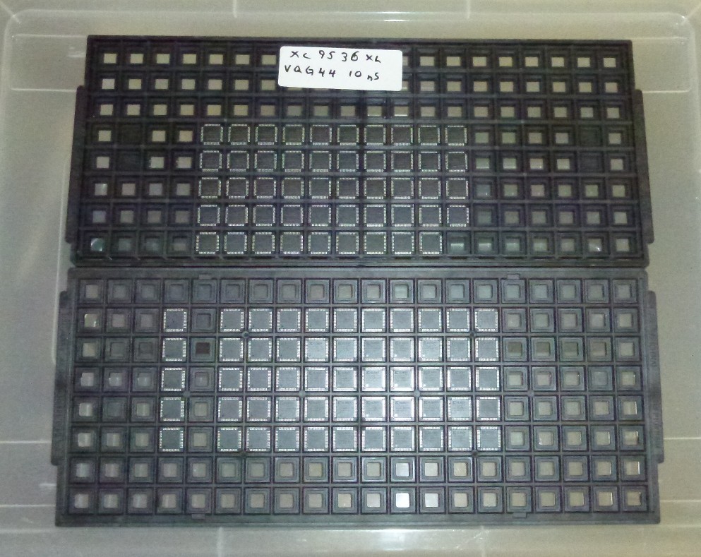
That's 104 Xilinx XC9536XL - 5 Volt tolerant 36 macro 10ns CPLD's.
I have ordered some level translators because I want a mix of 3.3 Volt chips and older 5 Volt chips like original CPU's.
I want the bus (backplane) to be 3.3 Volt LVTTL and not necessarily 5 Volt tolerant.
To achieve that I was going to use level translators for boards that had 5 Volt chips.
The translators I ordered are 9ns propagation delay data to data 10ns Output Enable (EO) to Data.
These CPLDs are 10 ns any pin to any pin so I might use them instead. This will also enable me to use the CPLD to rout signals making it easier to use single sided board.
Part of me doesn't want to use so much CPLD because it makes repeatability harder for others but I will use this as a starting point for flexibility.
If I use enough CPLDs (and I have 100 of them) the ordering of the signal on the backplane can simply be reprogrammed at a later time so that I don't have to commit to a signal bus layout to start with.
When I am more comfortable with a bus layout I will redesign using level translators instead of programmable logic at that later stage.
For now - looking at this -
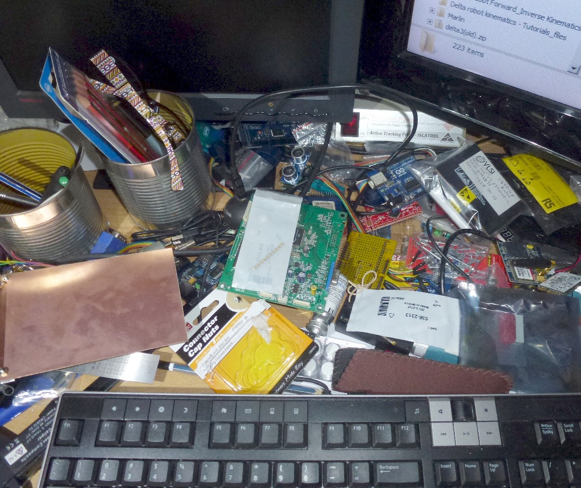
I might just to a tidy up of the programming / design desk while I am waiting for the connectors.
Well the parts (DIN41612 connectors) didn't arrive (still). I have some hope for tomorrow. I need to measure them and sort out clearances for screws in the front fascia.
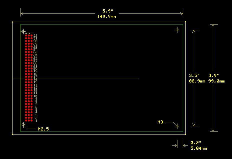
In the mean time I have started a rough draft of dimensions above.
I also played with some rivnuts or rivet nuts. It didn't work out to well for M3 without the tool -
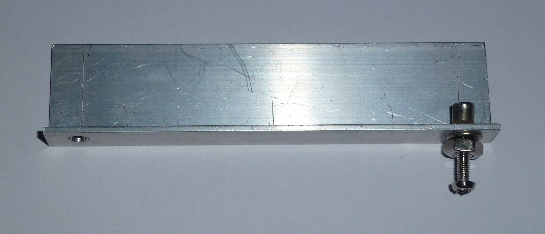
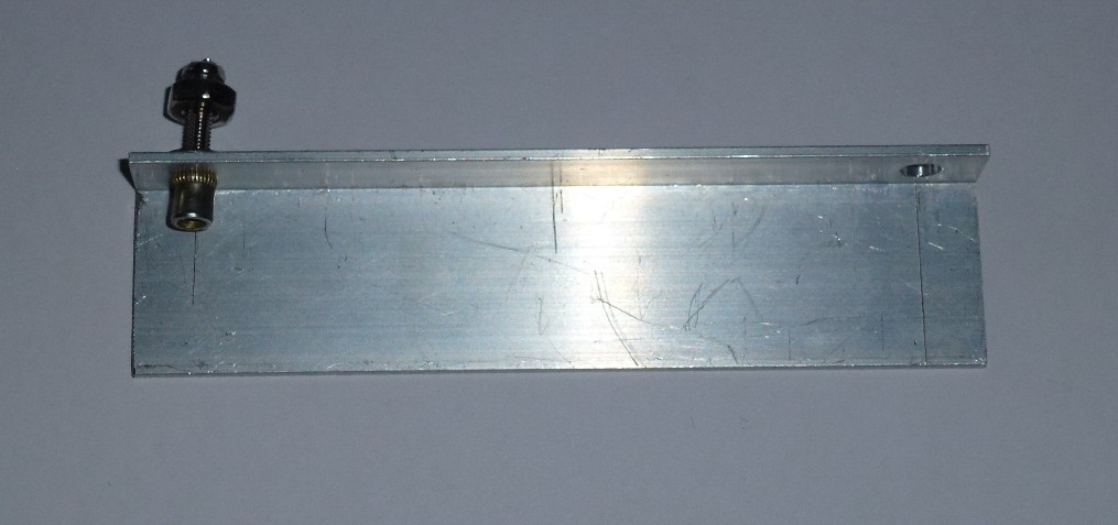
I tried to use a screw to compress the rivnut but the leverage of a M3 thread is to low and the screw head stripped so then I tried to compress it with a vice and it went bent ! :(
I will buy the too and try it.
I will first buy some countersunk rivnuts to try.
I decided to use DIN 41612 connectors as suggested by [Yann Guidon] in the comments. Thanks for the tip Yann.
These connectors are rated at 2 Amps per pin. The ones I was intending to use before I pulled them apart would loose voltage very quickly even at 1 Amp.
I would have had to gang many pins together and loose pin count for the bus.
Anyway we have had a cyclone near here, it's like a tornado but 500 kM wide. Thankfully this one wasn't fire tornado, Instead it flooded three quarters of this state and one quarter of the state below. The TLDR is that the parts ordered were NOT provided with scuba gear so they likely drowned along the way.
In the mean time I have been trying some EDA'a. I have been using ExpressPCB and it's good for toner transfer boards except you can't rotate a QFP by 45 degrees to make a DIP adaptor. KiCAD has been giving me a hard time but I will win this struggle lol. I haven't designed any boards as I am waiting for the DIN connectors to get dimensions.
Anyway - I had a look around the local hardware store to solve a problem.

It's not greatly obvious but the screw holding the PCB is adding to the width to the front fascia. The fascia is 25mm and the board will be 25.4 mm apart so the screws head will catch on the adjacent fascia. Also the handle is just too big and looks out of proportion.
These look like they may solve these problems -
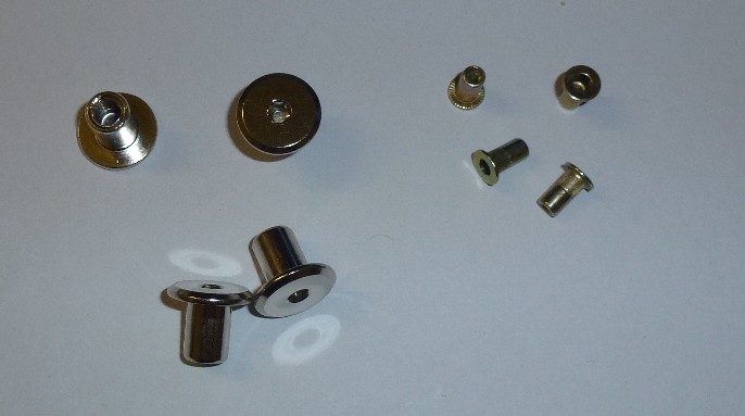
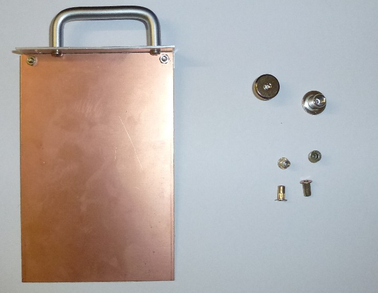
The lower pieces are Rivet Nuts or Rivnuts or Nut Inserts that I want to use to put through the side of the fascia to support the PCB. They compress like pop rivets.
I will try them and see.
Hopefully I can post back soon when the DIN connectors eventually arrive.
Connector - what to choose?
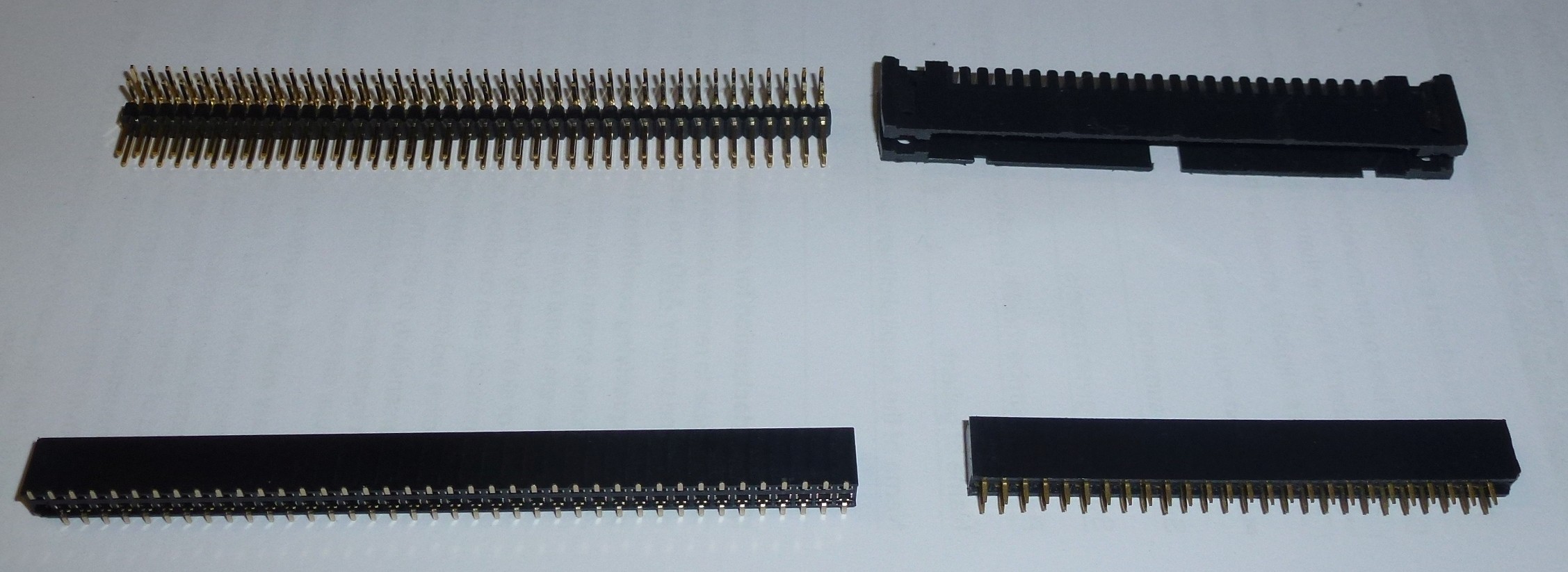
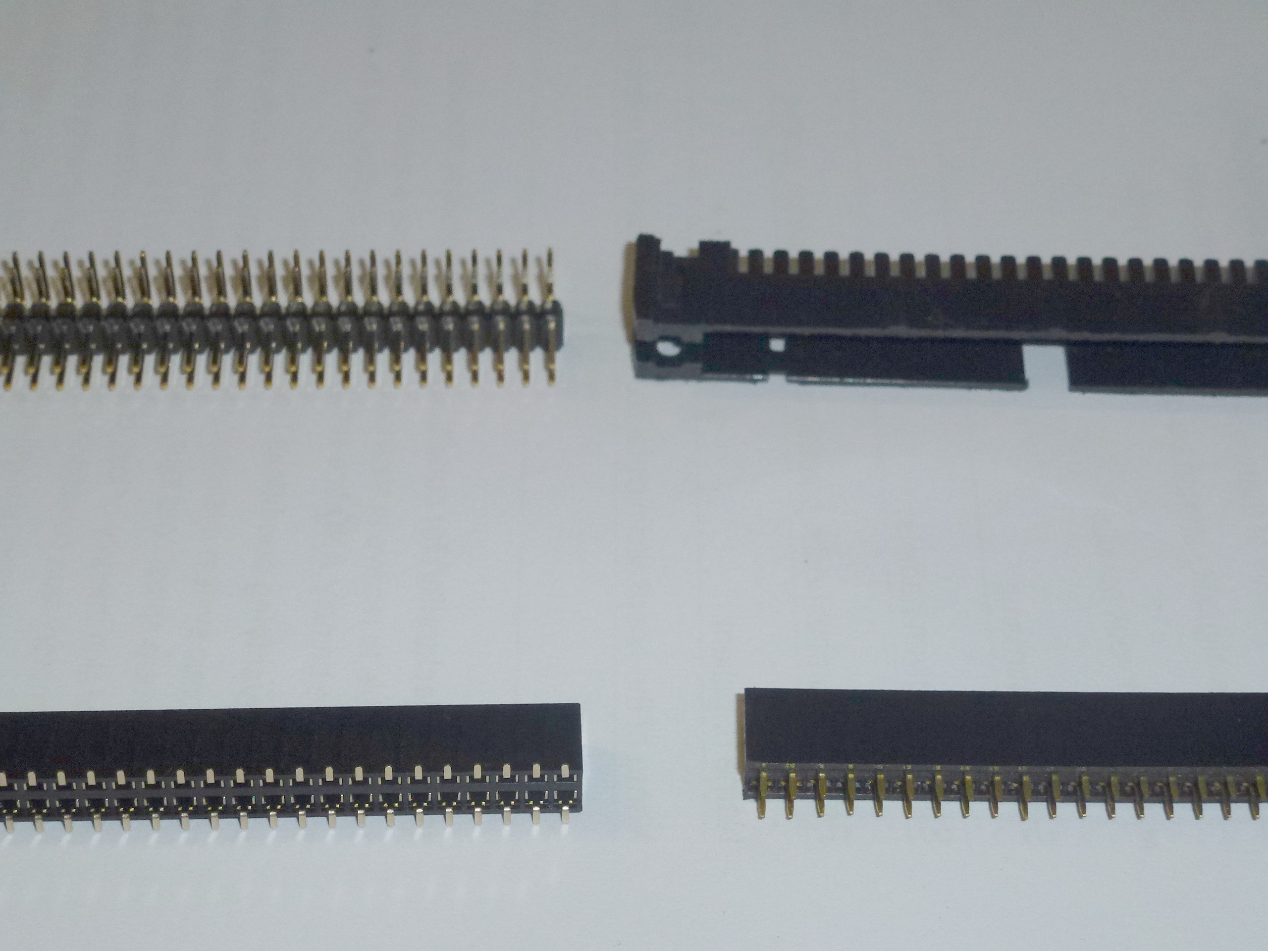
I was trying to decide between an 80 pin header (top left) or a 50 pin IDC style socket (top right).
And a SMT (header bottom left) or a through-hole header (bottom right).
It seems that the options are not as diverse as I expected.
Old 5 Volt chips need a bit of current to heat up their micro-steem-engines. lol
So I was wondering how many pins to connect together for the power feed. To that end I started pulling things apart and here is what I found -
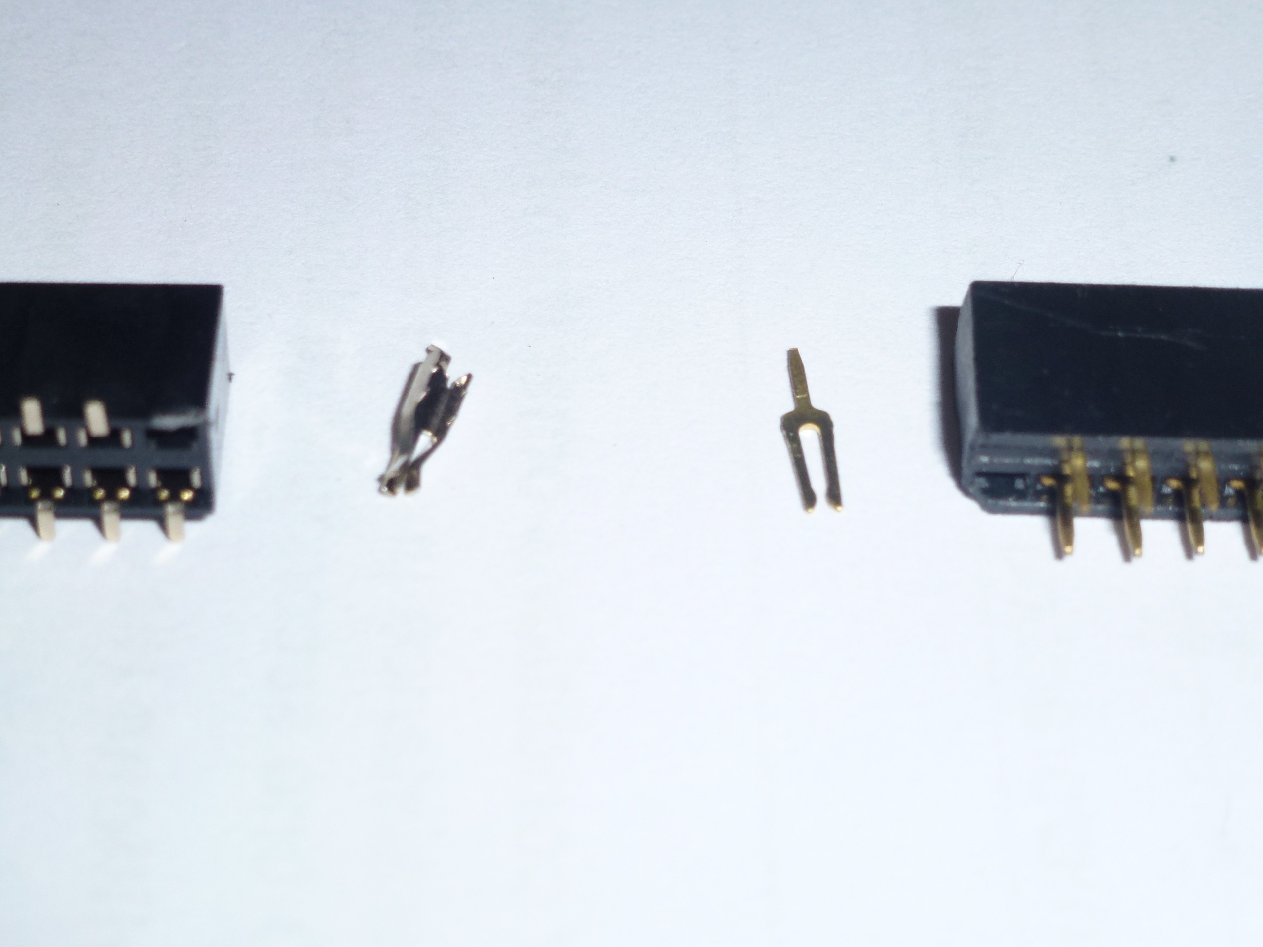
The contact surface area of the through-hole header is minuscule. The SMT header has about 6 to 8 times the contact surface area.
I really didn't want to use a SMT header because I worry about the connector lifting out of the solder.
So the problem now is - If I use the through-hole header then the 50 pin connector is not enough because I will need to use at least 4 pins for 5 Volts and 4 pins for ground. Perhaps I could just use a larger connector like 76 pins?
Even with the SMT header, I would probably use 2 pins for GND and 2 pins for 5Volts and I also wanted a 12Volt rail, so another to pins and thay makes 6. The Z80 CPU has 38 signal lined + 6 pins for power is 44pins so it only leaves 6 pins free in a 50 pin connector.
So I am going to do one of two things -
1) Just start with DIN 41612 like someone mentioned in the comments as they are rated at 2 Amps per pin - or use something different to start with and upgrade to the DIN later.
2) Make the layout so that it can be upgraded to DIN 64 pins (two rows A/c). I might put extra pins on either end for the power when using the cheaper connectors and just ignore them for DIN.
There are also other problems with the cheap connectors. They are not self-aligning like DIN so there will be some jiggling to get them in.
Option 2 above sounds good as it gives me the opportunity to find out how bad the cheap connectors are and recover by replacing them with DIN except ... I will be using cheap SMT connectors and the DIN are through-hole.
I am sending an order off in the next couple of days so I will see what I end up getting.
Create an account to leave a comment. Already have an account? Log In.
Now you need the matching Euro/DIN backplane :-D
I just spent an hour or so looking into this. What I found was they the Euro Card system is just about dimensions and I have chosen a card size that is close - 150mm x 100mm instead of the Euro Card 160mm x 100mm. I am going to stay with 150mm x 100mm because it's a more common size now and cheaper for that reason.
The DIN you refer to seems to be DIN 41612 which specifies a range of one type of connector. I can get these at about $10 a plug/socket pair for 96 or 64 contact connectors. This is appealing for me but just for now I am going to use what I have lying around rather than add expense to this Version 1.0
What I will use in Version 1.0 is 50 way (25x2) right angle locking 0.1" like headers with the locking tabs remove. That way the same can be duplicated without the card rack by just using IDC connectors and cable. The back-plane will have the PCB type matching headers.
Thank you for the heads up and I will keep this in mind for a future version.
For now I will be using single sided boards and CPLD to rout the traces to the connector and also glue so 50 pins is a good size for the CPLDs that I will be using.
At least the DIN 41612 connectors fit the 100mm width for the next iteration :-)
What sort of computer will you develop ?
The computer is going to be very modular to start with so that it can be re-configured to different systems. There will be programmable logic for glue that can be reprogrammed. Each board will have 3 or more small CPLD's (like small FPGA).
My first computer project will be a Z80 system but before that will be a Chip Tunes card with one or two AY-3-8912's and then a speech card using a SPO256.
I will make the debug card first, it will be able to drive the chip tunes and speech chip as it will be able to take full control of the bus system. I am deciding between an ATmega328 or an ATmega1284 for the USB debug card or even a ATmega2560 for the pin count. The 1284 or 2560 would also be able to program an onboard parallel flash that could also hold the bootstrap or this may end as a separate card.
Hey, Thanks for the tip! I ended ordering some DIN 41612 connector as they specify 2 Amps per pin and that is important for any old 5 Volt chips because they consume much more power than modern chips. From the pics you can probably see that I would have ended up with voltage drop issues with the connectors I was going to use.
Now for you next task (LOL) can you convince me to go with the Euro-card PCB dimensions 160x100mm? instead of the 150x100mm dimensions that I have chosen *because* there cheaper from China?
I made a PCB cutter so I can use any size now. I buy PCB in 305x305mm. What's more available where you are?
Wow look's great! Have you considered giving the aluminum some kind of paint or plating perhaps? That would look really cool if wrapped in vinyl too, could get a nice retro 80's look/feel or something more modern too like carbon fiber; might have to mitigate static from the vinyl when you put in or pull in a card though, should be an easy fix.
It looks great the way it is too, gives it a real nice 40's-60's look and feel. Just wanted to share what lept into my head when I saw it. I'd love to see you populate and wire up those boards, keep it up!
How about some woodgrain vinyl? Make sure to add lots of blinkenlights as well!
I'm thinking powdercoat the board bulkheads in C64 beige and the front facing chassis pieces in brown. Liberally apply rub-on lettering.
I think I can get wood-grain veneer from the hardware store. I might give that a go later.
I probably wont go to the expense of power-coating but I definitel like your color scheem.
Definitely!!! I was thinking of putting 8 LEDs up the front and a CPLD that does nothing but flash them - just for that retro 80's look.
I thought of those LED arrays with 10 leds but square holes are hard to drill - perhaps a whole stack of good ol' 5mm LEDs with bezels.
I definitely will be adding some blinking lights. I have never herd of a vinyl version of wood-grain. Can you tell me more about it please?
I doesn't look that good IRL lol. Many scratches and my metal work isn't so good. Paint would be easy and I may do that but paint tends to be not so good at sticking to metal.
I was going to make some gammon logo to put on the top but I forgot. I was going to print in color with a laser and then transfer that to the top using a laminator. I could still drill the pop rivets and do that later.
The retro 80's look is an idea and perhaps I can make it colorful but how do I give it big hair, bright colors and leg warmers?
I have to make two boards and the back plane so that I can align the back-plane. The first board will be the USB debug bus controller.
It's a start lol. A bit messy with the metal work but it's just a 'fun' thing. I might try and fine different handles though as these ones look too big.
Become a member to follow this project and never miss any updates

 deʃhipu
 The Big One
 tonyo
tonyo
 SukkoPera
Wow it's getting seriously nice ;-)