Bud Bennett
-
First Pass Evaluation
07/08/2025 at 21:30 • 0 commentsIt's 2025-07-08. I received the core probe PCB, the generic micro USB DB and the buck converter DB. They all work, but I will need to make changes on the daughter boards to prevent problems when stacking onto the core probe.
The Probe Evaluation:
I did not take rigorous data this time. The probe performed as expected, with a few problems that were easily resolved. I had a couple of issues during assembly. I did not have the 412Ω or 3.92k resistors in my inventory. Luckily, I measured two 3.9k 1% resistors to be 3918Ω and stacked two 820Ω resistors on top of each other to get 411Ω. I did not have the 620mΩ snubber resistors either, so 1Ω would have to do.
When I powered it up it drew 25ma or 60mA randomly as I fiddled with the board. Clearly there was an intermittent connection somewhere -- it turned out to be the power pin of the LTC6269-10. A bit of work with the hot air rework station fixed that. I now draws 60mA and I get a signal out when a signal is applied to the input.
Then I noticed that there was a difference of a few hundred mV between the positive and negative supply rails. The rail splitter opamp was oscillating (a sawtooth waveform) at 10kHz. I disconnected the 10uF cap at the output of U4 to no effect. Then I replaced the FB3 ferrite bead with a 3 Ohm resistor and the oscillation went away. Lesson learned. The small resistor is 10X the resistance of the bead, but there is not much current flowing through it -- even at full scale output voltage swing the effect on the GND voltage will be just a few hundred uV.
After a quick check to see if the gain was correct I calibrated the DC common mode and the two AC gain paths without any issues. It did not require any change in the large attenuator capacitors, or any additional capacitor in the open 0603 capacitor location. I had calculated those values based upon the -7.5% change on the 10pF input capacitors and it proved correct this time as well. It also helped to have a 15.5pF trim range.
I was able to trim the output offset to less than 1mV, using a DVM. This offset moves several mV as the supply voltage changes a few hundred mV. I would not recommend swapping DC-DC adapters, that will have different voltages, if you are going to implement the offset adjust feature. But using a daughter board with a regulator should be fine.
Overall DC gain was a smidge high -- about 1%, which I attributed to my stacked 820Ω parallel kluge. I can't measure AC gain much past 10MHz, but it was good to that point. I applied 20Vpp (the max of my function generator) and did not see any clipping at the output.
The noisy output is still there. I can see about 100mVpp of hash at the output when the scope is set to 10X mode.
In short, this probe looks nearly identical to the old one. That's good!
The Buck Converter Daughter Board:
l built two versions of the buck converter -- one with an RT8259 chip and another with an RY8310 chip. They are nearly identical performers. Digikey sells the RT8259 for more than $1.5, while LCSC sells the RY8310 for around $0.10. There is a side benefit to the RY8310 in that it doesn't require a freewheeling Schottky diode at the switch node.
Both boards worked well. They both were almost exactly 5.3V at the output. There was a 20mVpp 1.4/1.5MHz square wave ripple at the output, as expected. The load and line regulation was excellent -- about 2-mV change for 50mA change in load current, and about the same 2mV change as the input voltage changed from 9-12.5V. The overhead was also very good as both converters would not drop the output voltage until input voltage was below 6V.
The RY8310 was more efficient -- 80% @12V, 85% @9V. The RT8259 was about 5% lower. Still not bad. At this low current (60mA) both boards remained cool, as they should because they only dissipated around 150mW.
Pairing the buck converter DB with the probe:
I tried to mount the RT8259 daughter board under the probe and immediately found a problem. The two input voltage pins on the DB are through-hole and are located at the back of the DB where the SMA connector is located on the probe. The wires running from the DB to the trigger board must be soldered to the underside of the DB and might short to GND if they contact the housing of the SMA connector or its rather large pins that are soldered to the back side of the probe PCB. This issue will require a change to any daughter board that has components mounted on the bottom side, and the input voltage pins will need to be relocated to the front of the DB and made surface mount only to the bottom side of the DB.
By carefully soldering the power leads to the DB and mounting the DB above where it would interfere with the SMA connector I was able to attach the DB to the probe. When I powered it up I could not detect that it was being powered by a switch mode converter. It helps that there is a ton of noise at the probe's output. It might show up with a spectrum analyzer, but I don't think so. The back side of the probe has a solid ground plane to act as a shield to any switching noise produced by the converter.
I think that this combination of switching converter and USB-C trigger board will be my goto solution to powering the probe. It's small and cheap and cool compared to the LDO solutions.
Putting the Probe into the Case:
The bottom housing of the case had to be modified in order to get the probe with DB attached mounted properly. Eventually, I got to the point where everything snapped together (without the trigger board attached yet.) Here is the result:
![]()
The case is yellow to match the color of the first channel of the scope. I cut out a section near the LED indicator so it would allow a brighter glow from the LED. It is not as bright as the photo would suggest. I'm pleased with the result.
-
The Bane of Mutual Inductance
06/23/2025 at 19:16 • 0 commentsI've been simulating the daughter board voltage regulators lately. It seems like the data sheets for these LDO regulators, and the switchers too, don't account for any inductance in the power input leads. That's not the case here. I expect almost all users (except maybe some that employ batteries for power) are going to have relatively long -- around 1 meter -- leads running from the power adapter. This creates both lead inductance and mutual inductance between the leads if they are close together.
The lead inductance depends upon the diameter of the wire and its length. The mutual inductance depends upon the distance between the two wires. All of this can be modeled in SPICE.
![]()
It is not too difficult to create a model for the input power leads that depends upon the wire's AWG and length. The coupling between the wires depends upon their separation, which is pretty small for these thin wires, and therefore K is at the high end of the range (between 0.7 and 0.9) I believe. The interesting thing to note is that the higher/thinner AWG tends to have a higher inductance, but also a higher resistance that tends to lower the Q of the tuned circuit. For example, a 1m long 26AWG wire has an self inductance of 1.68µH and R=128mΩ, where the same length of 30AWG has a self inductance of 1.78µH and R=327mΩ.
I first discovered this when I simulated the LP2951 LDO. The data sheet shows a pretty basic application:
![]()
A minimal input bypass cap and 2.2uF for the output. And this is what the data sheet has to say about bypassing:
A bypass capacitor is recommended across the
LP2950/LP2951 input to ground if more than 4 inches of
wire connects the input to either a battery or power supply
filter capacitor.
Input capacitance at the LP2951 Feedback Pin 7 can
create a pole, causing instability if high value external
resistors are used to set the output voltage. Adding a 100 pF
capacitor between the Output Pin 1 and the Feedback Pin 7
and increasing the output filter capacitor to at least 3.3 F
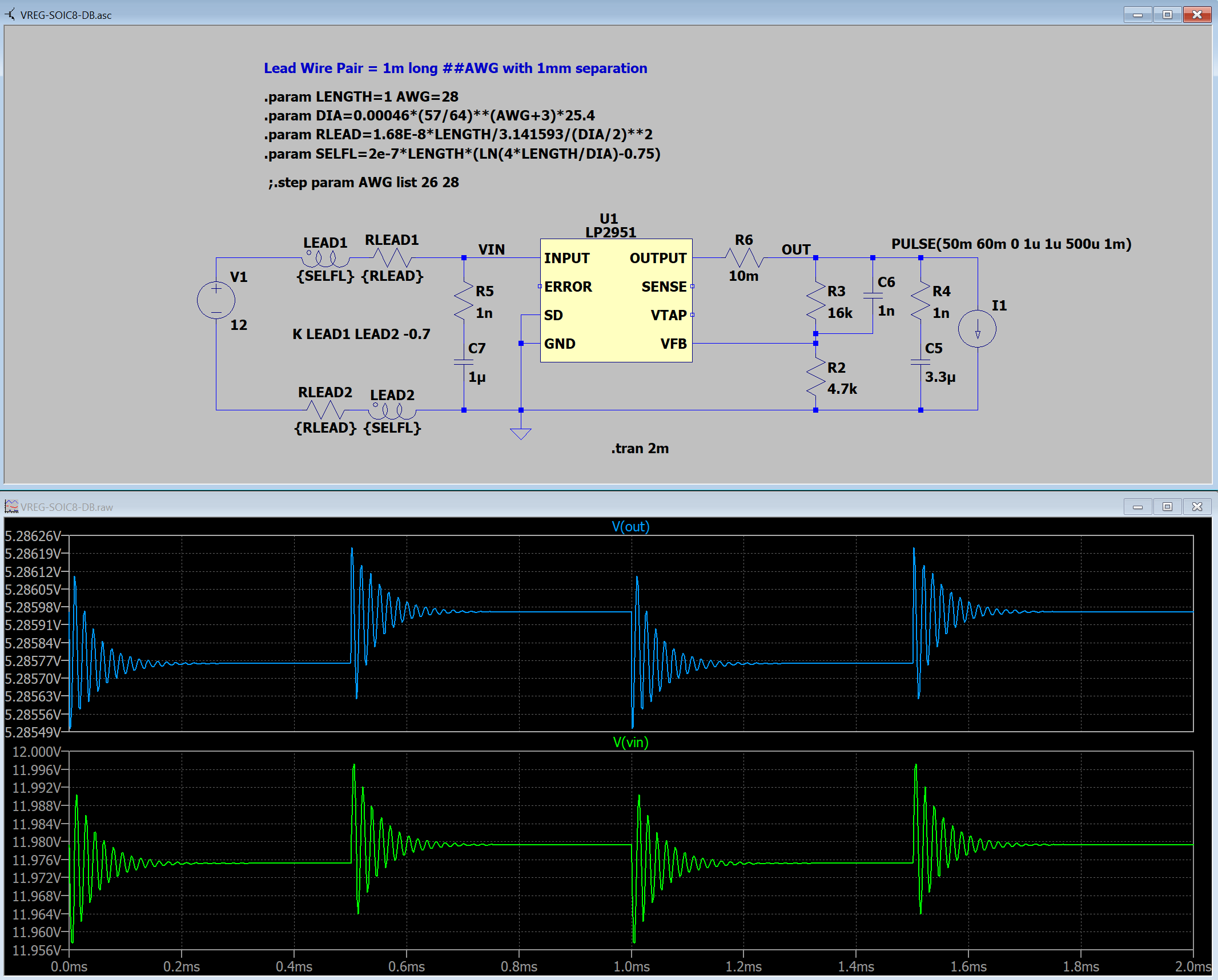
will stabilize the feedback loop.So this is the simulation result when I used the suggested values for ceramic capacitors, 1uF at input and 3.3uF at output, and set the length of the input leads to 125mm (~5in) and AWG=28: (load current is 50mA)
![]()
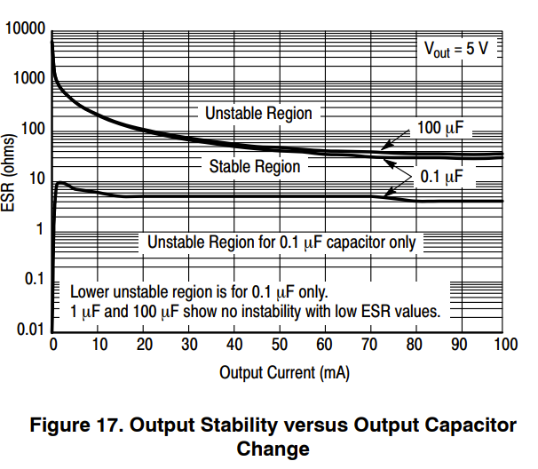
That doesn't look too good. The data sheet specifically states that low ESR bypass caps can be used. This is presented in a plot:
![]()
If I set the length of the input leads to 1m the oscillation disappears for steady state (due to the lower Q), but still looks pretty ringy dingy when excited:
![]()
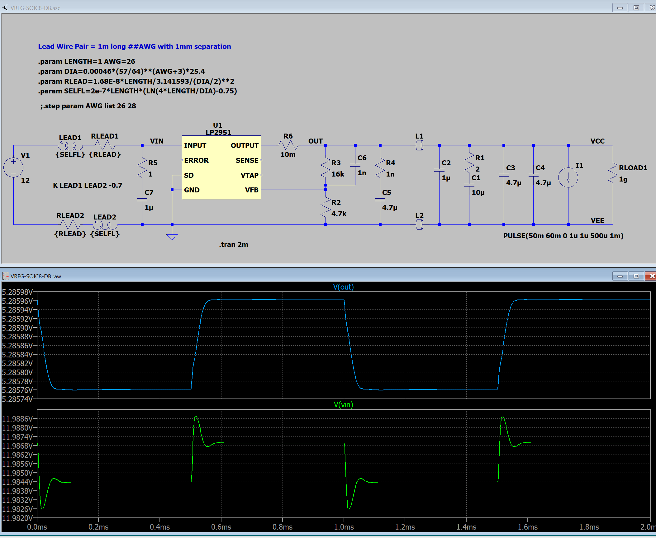
In order to kill any possibility of oscillation a 1Ω snubber resistor should be added to the input capacitor. Then things look pretty good, even when driving the inductive looking load of the slim probe.
![]()
That underdamped response is due to the ferrite bead inductance and doesn't go away with increased snubber resistance. There apparently is no need for any large ESR output capacitor, but I will keep a discrete resistor in series with the output capacitor just in case.
Mutual Inductance Effects on the Buck Converter Daughter Board Design:
After all of that prior discussion, I won't bore with the details here. The problem I have is that I was not able to simulate the buck converter (off-brand manufacturer with limited modeling resources) and released the design without adding any discrete snubber resistors.
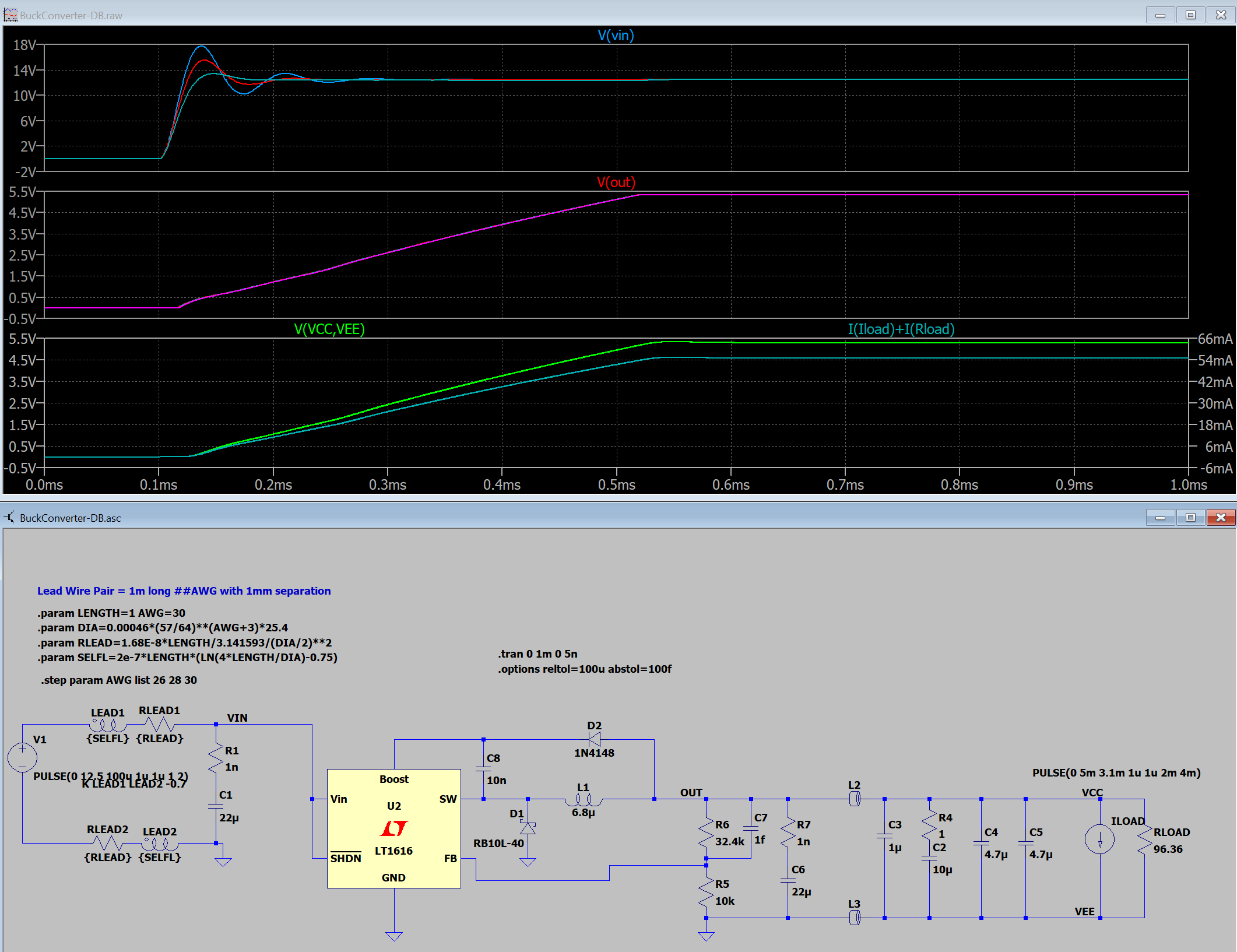
I fudged a simulation by using a similar switching converter IC model that ADI had a model for: the LT1616. As expected, the buck converter did not like the inductance of the input leads either. But it appears that the snubber resistors might not be necessary. The only way to tell is to build it and test it.
I put the lead inductance model in series with the buck converter input and checked in over various simulation parameters. There is one interesting phenomenon that show up: if you connect a powered adapter to the daughter board there's a chance that you can damage the daughter board. Here's one case where having cheap 30AWG leads from the adapter can save you. I ran a simulation of this event using 26-30AWG lead wires. Here is the result (without a snubber at the input):
![]()
The smaller AWG wire doesn't produce as large of input spike because the higher wire resistance de-Qs the L-C tuned circuit at the input. The way to avoid this scenario is to solder the adapter lead wires to the daughter board -- the rising voltage waveform will be much slower. Otherwise, even a 0.5 Ohm snubber resistor in series with C1 will do the job.
-
Daughter Board Variety
06/21/2025 at 21:03 • 0 commentsThere are plans for 5 daughter board variants:
- Generic microUSB interface. 5V in, 5V out.
- Discrete voltage regulator (see previous log.) 7.5 - 12V in, 5.3V out, or 20V in 15V out.
- SOT89 LDO regulator. 7.5 - 12V in, 5.3V out.
- SOIC8 LDO regulator. 7.5 - 12Vin, 5.3V out, or 20V in and 15V out.
- Switching regulator (buck converter). 7.5 - 12V in, 5.3V out.
They all fit onto the 13x13mm daughterboard dimension. If none of these tickle your fancy, then make your own.
Generic micro-USB:
There's not much going on here. Just a standard micro USB (B-type) mounted on the edge of the daughter board as so:
![]()
The 5V output connects to the probe power supply inputs through the header pins. The connector is an Amphenol 10103594-0001LF -- hopefully easy to get and not too expensive. This is probably what I will use for my slim probes since I have jiggered my wall adapters to output 5.25VDC.
SOT89 LDO Daughter Board:
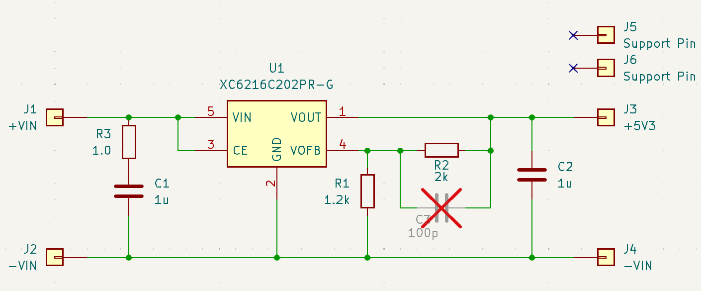
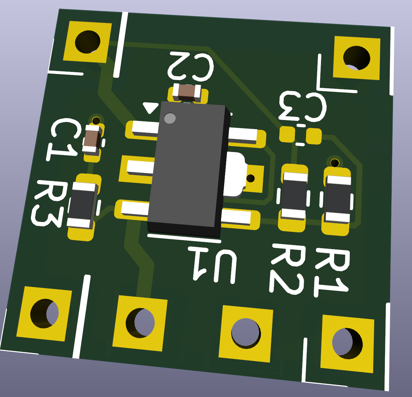
This board uses the same LDO as what Paul used for his original probe. The LDO is an XC6216 adjustable voltage regulator IC, that comes in a SOT89-5 package.
![]()
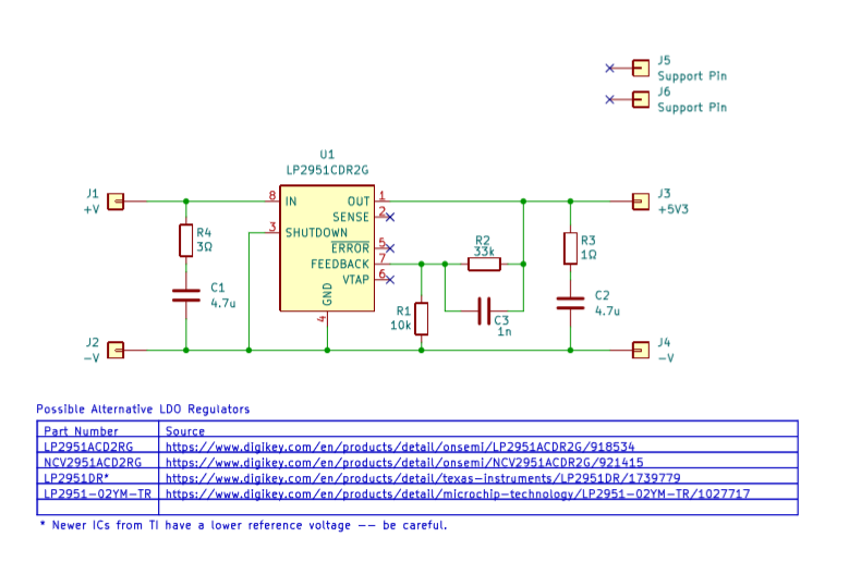
There are a few alternative LDO ICs that will work as well, if you can't get the XC6216.
![]()
The SOT89 should be able to handle the power dissipation easily.
SOIC8 LDO Daughter Board:
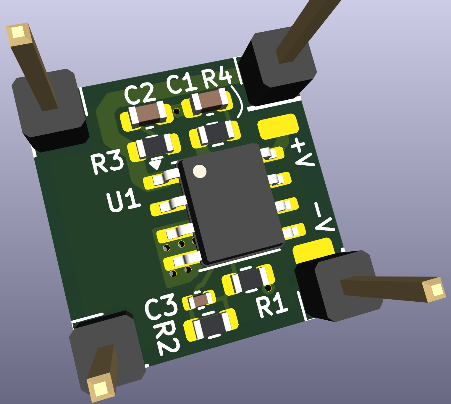
I used a widely available LP2951 voltage regulator that comes in a SOIC package option. It's a bit large, but it fits. [2025-10-21] Added a better snubber at the input.
![]()
There are three main manufacturers: TI, On semi, and Micro Chip. It is relatively inexpensive, around $0.50/each in low quantities.
![]()
Buck Converter Daughter Board:
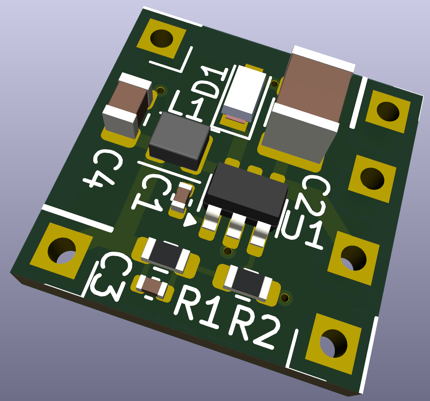
I designed this board just for grins and giggles. It should be much lower power dissipation than the LDO alternatives. But it might be too noisy to be located so close to the probe circuitry. The switching regulator is a Richtek RT8259 (with RyChip RY8310 as a second source.) It switches at 1.2-1.4MHz, which allows for small components.
![]()
![]()
-
VREG DB Survival
06/16/2025 at 20:52 • 1 commentI received an order of 5 USB-C trigger boards a couple of days ago. The available voltages from the trigger board are 9V, 12V, 15V and 20V. I have two bona fide USB-C adapter/chargers, both from Samsung, one is 25W and the other is 45W. I also have two clones of Apple adapters with USB-C jacks and a USB-C adapter for the Raspberry Pi 4. The first thing I did was to plug a trigger board into the USB-C port of my desktop computer. The little blue LED on the trigger board did not light up and the voltage output read 5VDC. I expected this behavior.
Then I connected the trigger board to the 45W adapter. The LED indicator lit immediately and the trigger board put 9VDC at the outputs. The problem with this is that the trigger board is set for 12V output. I'm a bit confused at this point so I plug the trigger board into the 25W adapter. The LED indicator eventually lights up after maybe 5-10 seconds. The output voltage is 12VDC. The two Apple clone adapters both light the LED immediately and put out 12.4VDC. The RPi adapter only puts out 5V. Now I'm really confused as to what is happening.
I trolled the internet as to what the issue could be but found nothing useful. At this point I have zero trust that the trigger board will output the correct voltage and it dawns on me that the circuit I designed probably won't survive in the wild without some improved robustness. The VREG daughter board must not fail or damage the expensive core probe circuitry if/when 20VDC is applied to its supply pins!
When I was designing circuits for a living I worked with some very experienced people (you might even call them legends.) They taught me a couple lessons:
- The best circuit designs are the ones that apply to the broadest range of applications.
- Sometimes a circuit's survival is more important than its performance.
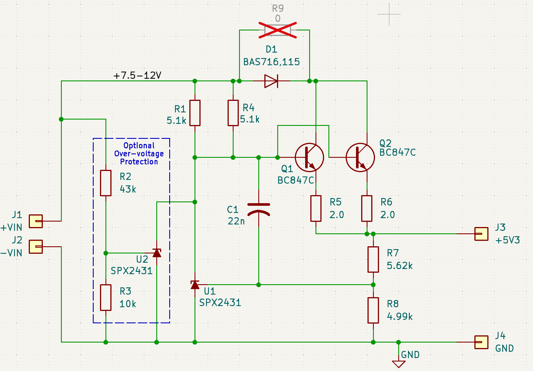
The PCB is tiny, only 13x13mm. It is also a DIY project, so 0201 components are out of consideration. I figure I could add a single SOT23 (not the difficult to solder SC70) and 2-3 resistors if most of the resistors could be 0402 size. After toiling away for a couple of hours on LTSpice I finally had a Eureka moment -- using another TL431/TL432 as a reference/comparator in the following circuit:
![]()
This worked like a charm in LTSpice with behavioral models for the TL432. When the input voltage exceeds 13.2V the voltage at the REF pin of U2 exceeds 2.5V, and U2 will draw a lot of current from its cathode pin, effectively shutting down the output voltage at J3. U1 will attempt to compensate, but all it can do is reduce its current until it goes to zero. R4 is used to share the current through R1 and keep the power dissipation below the 100mW limit for 0603 resistors. This action saves Q1 and Q2 and R1 from burning up when 20V is applied. D1 protects the components against reverse polarity inputs.
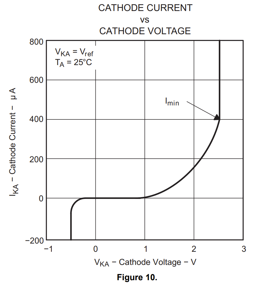
Then the gloom settled in as I realized that the behavioral models might not exhibit all of the correct behavior of the TL432. Here's the problem: Where is the current coming from to power U2? I measured pA of current into the anode of U2 using the first behavioral model from TI. The second SPICE model from TI sucked a whopping 1uA from the anode pin until it began to override U1. Still not correct.
TI publishes the anode current vs voltage in its datasheet:
![]()
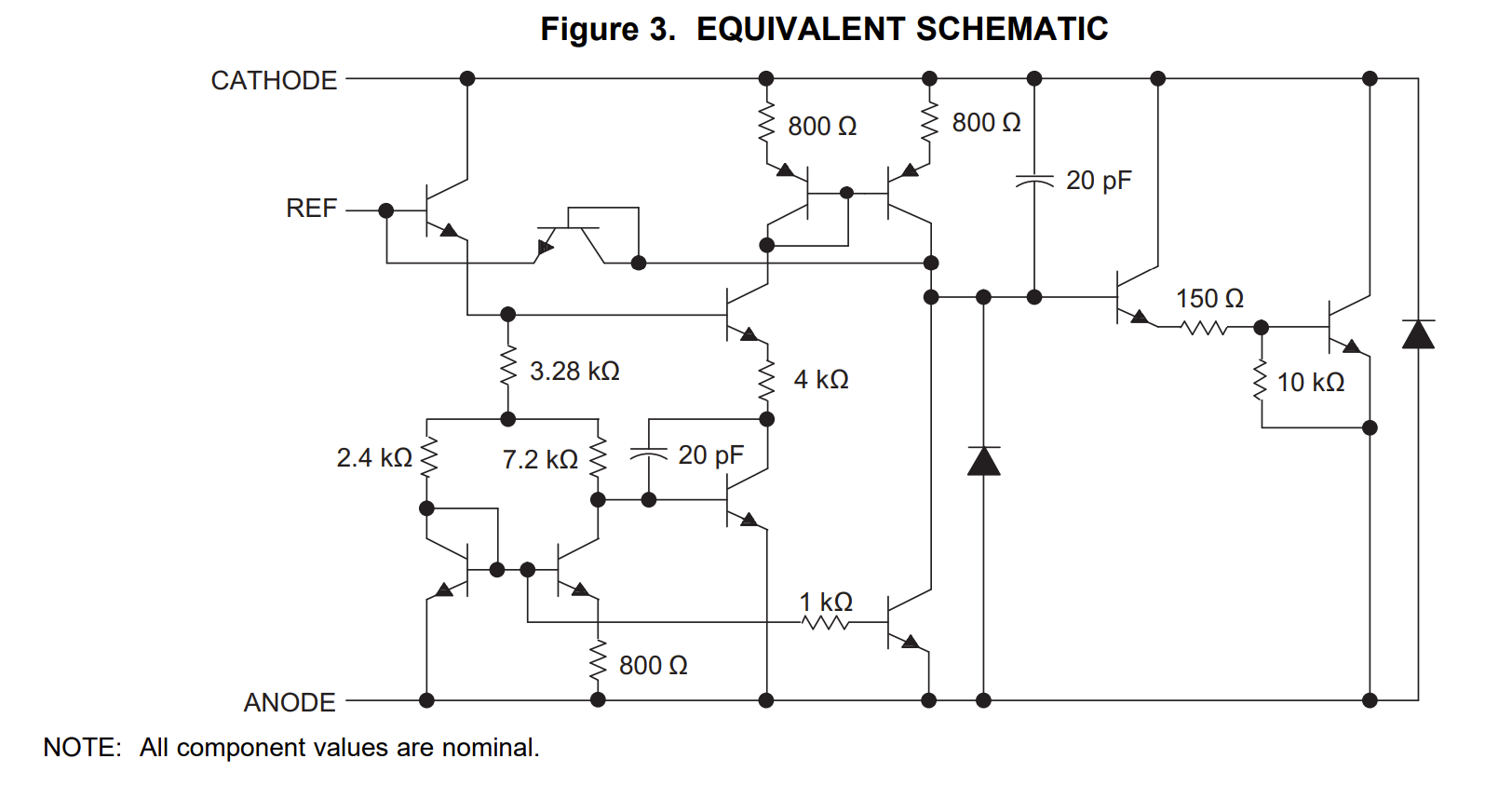
That's not really helpful. Fortunately, TI published a schematic, with values, of the TL431 in the datasheet:
![]()
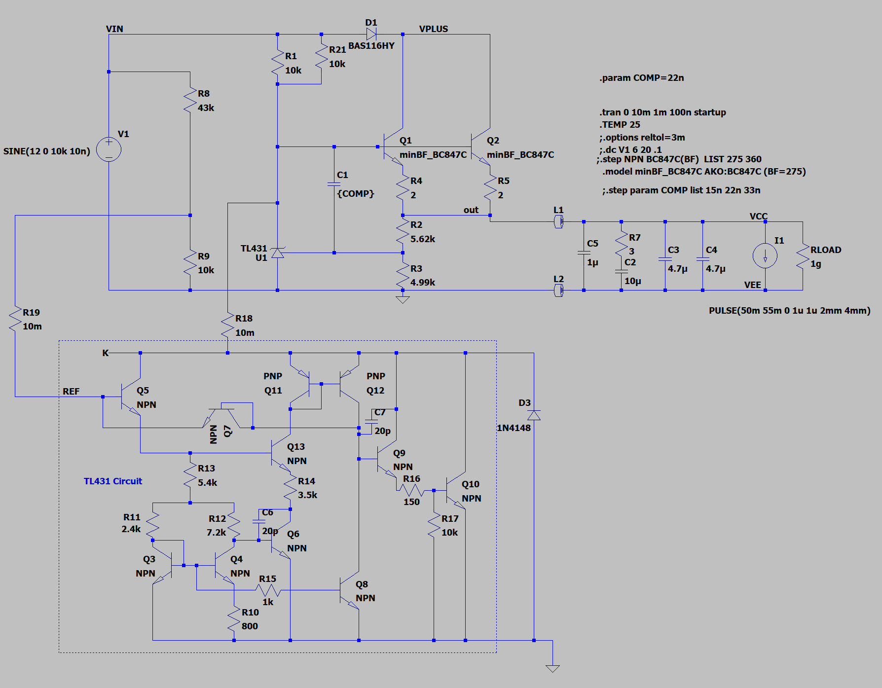
And I created a schematic to imitate U2 in LTSpice:
![]()
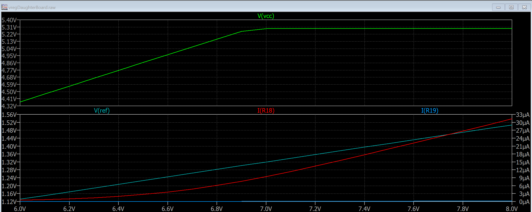
I used generic LTSpice NPN and PNP models which forced me to change R13 in order to get the circuit to regulate at 2.5V. Now I expected the currents at REF and K to be more realistic (but probably not perfect.) A DC sweep of V1 confirmed it:
![]()
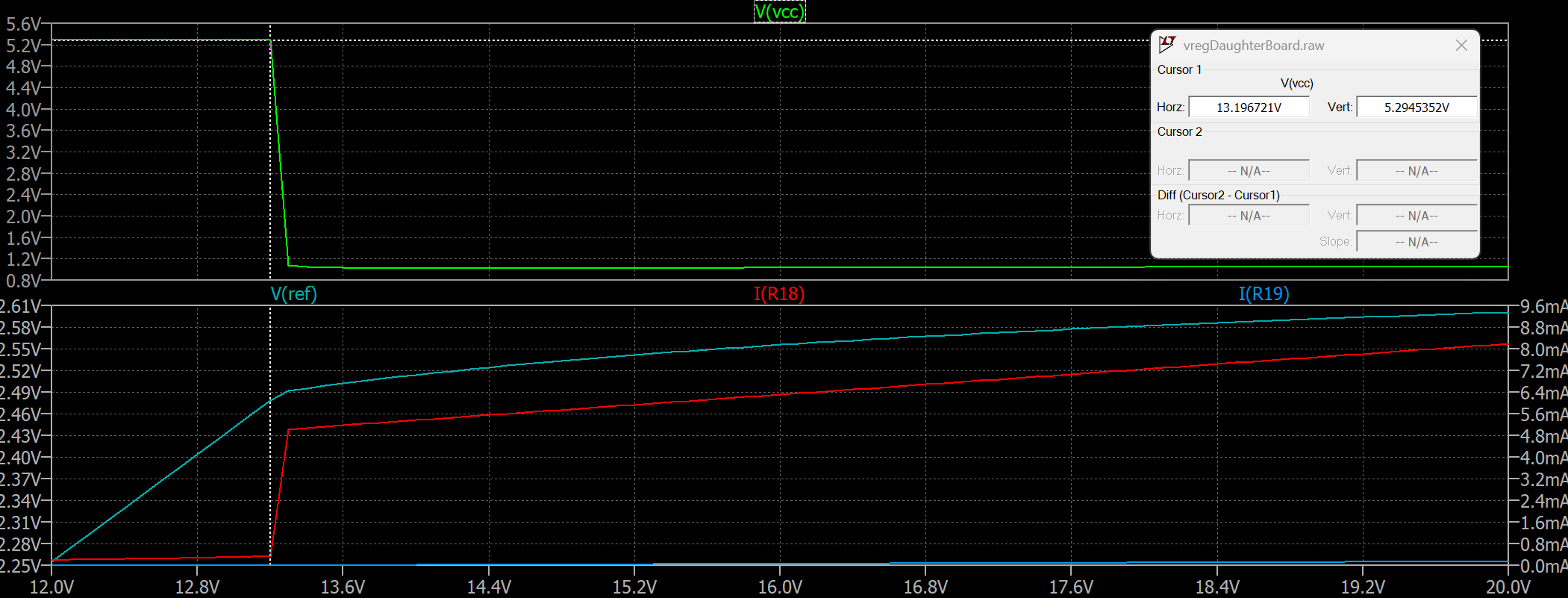
R18 monitors the current into the anode and R19 monitors the current into the REF pin. There's no contest...nearly all the current is going into the anode. This gives me some confidence that the over-voltage protection won't interfere with the normal operation of the regulator until the input voltage exceeds 13V:
![]()
And that is apparently correct -- the over-voltage monitor doesn't impact the output voltage until the input voltage exceeds 13.2V. Note that the output of the regulator drops to about 1V. That is because U2 requires some voltage across its anode in order to continue to function.
I ran several simulations to determine the performance of this circuit.
- The values of R1 and R4 should be raised to 10k with input voltages of 12V. This keeps the power dissipation lower in normal operation and limits the dissipation with 20V input to less than 33mW in R1 and R4. With R1, R4 = 5.1k, the power dissipation increases to 66mW at 20V, which is still acceptable for a 0603 resistor.
- Q1 and Q2 are the big power hogs. They will dissipate 200mW/each when dealing with 12V inputs. They will get hot -- around 110C.
- The compensation capacitor, C1, is awfully large. It is OK though because the big tank capacitors across the output and opamps will take care of any fast transients. I'm trusting the SPICE behavior models to properly emulate frequency response (I used 3 different models) but can't help wondering about what the real circuit will need for compensation.
- If you need to use an adapter that outputs 7.5V-9V then the standard issue TL431 requires too much current (1mA) in order to regulate. This lowers the values of R1, R4 and causes them to exceed their power dissipation limits if a 20V fault occurs. There are many (~75) lower current alternatives to the old TL432 that require less than 200uA to operate.
All of this protection was put in place because I can't trust the trigger board to produce the correct output with various USB-C adapters. If you have a dedicated adapter or non-USB-C adapter, then all of that protection can be depopulated.
There are two tables on the VREF daughter board schematic: one for suggested values for R1, R2, and another table for suggested lower current alternatives to the TI TL432. I also suggest that a 9V adapter (or trigger board set to 9V) be used to power the probe. A 12V adapter will cause about 400mW of dissipation vs. only 220mW with a 9V adapter.
Note: The TL432 is used in this circuit. It is the same device with a different pinout than the TL431. The SPX2431 is in my inventory, and has the same pinout as the TL432, so that pinout is used. I'll put a note on the schematic too.
A Slim 10x 100MHz-10MHz-1MHz Differential Probe
A needed update to an older project.