 Bud Bennett
My first attempt at a differential oscilloscope probe was over five years ago. Its progress is documented as “A 10X 100MHz Differential Probe” here on Hackaday. It’s time for an update. I was impressed with the design modifications that Chistoph and Wolfgang pursued, but apparently never finished, so I recently decided to continue on with their initial ideas for improvement, but make it generally more useful for the DIY community rather than those with the wherewithal to have a Keysight Oscilloscope. If you have a Keysight scope, here's your probe (only $1900).
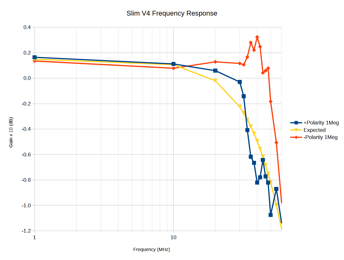
Paul built a 100MHz probe and a 10MHz probe. He published his notes and measurement results here.
Changes:
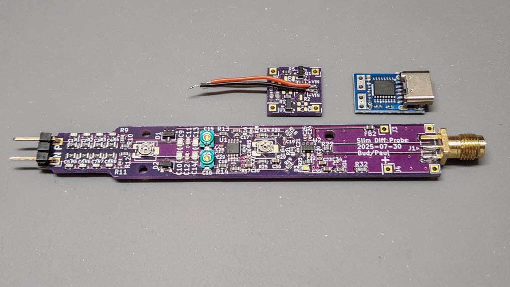
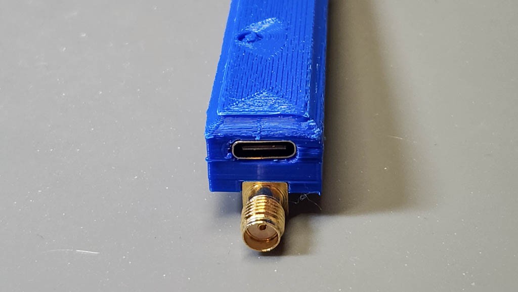
- A slimmer layout. Roughly 13mm x 100mm, making it less blocky and more probe-like. The longer probe will also make it easier to hold and handle while manually probing around circuits.
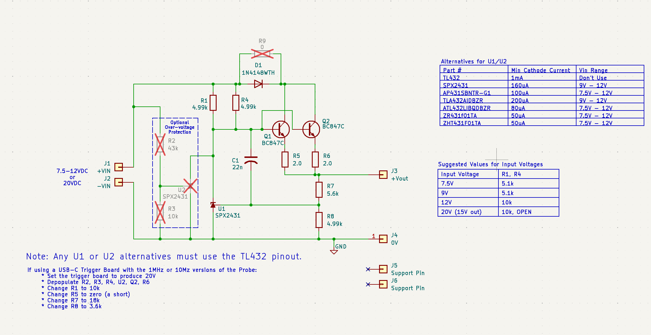
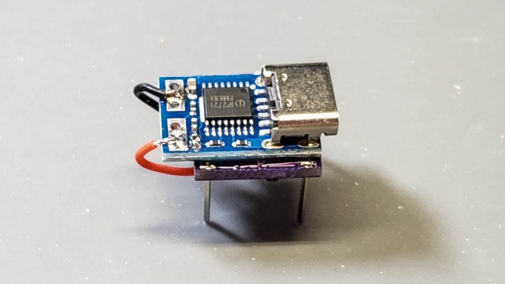
- Modular. The previous design had two incarnations — mine and Paul’s. Mine was powered by an isolated 5V wall adapter. Paul’s power was a 7.5V-12V wall adapter, which required an on-board voltage regulator on the probe. This new probe uses a basic core probe that requires 5VDC, or 15VDC isolated power, but it can be configured to accept various USB connectors and voltage ranges through the use of separate daughter boards that plug into the rear of the probe’s core PCB. Right now there are 5 daughter boards: a standard micro USB-B 5V interface, three voltage regulators that will take 7.5V-12V (bare wires) as an input and deliver 5.3VDC to the probe, and a USB-C trigger board that provides 9V or 12V to the voltage regulator daughter board. Something for everybody. The daughter boards are small, and therefore relatively cheap, made with easy to get ubiquitous components. Beware, the reverse polarity protection has been removed.
- [2025-07-08] Added two lower bandwidth versions: 10MHz and 1MHz. Both versions have increased differential input voltage range (140Vpp). These versions require a 15VDC power source, which is easily available from a USB trigger board.
- A power indicator LED. Meh.
- Offset adjustment. Up to 35mV of adjustment to the output voltage of the probe. This is not without some degradation in performance — both gain accuracy and supply rejection, along with other untoward negativities. But it is optional if you decide it is not worth it.
- Improved common mode rejection at higher frequencies.
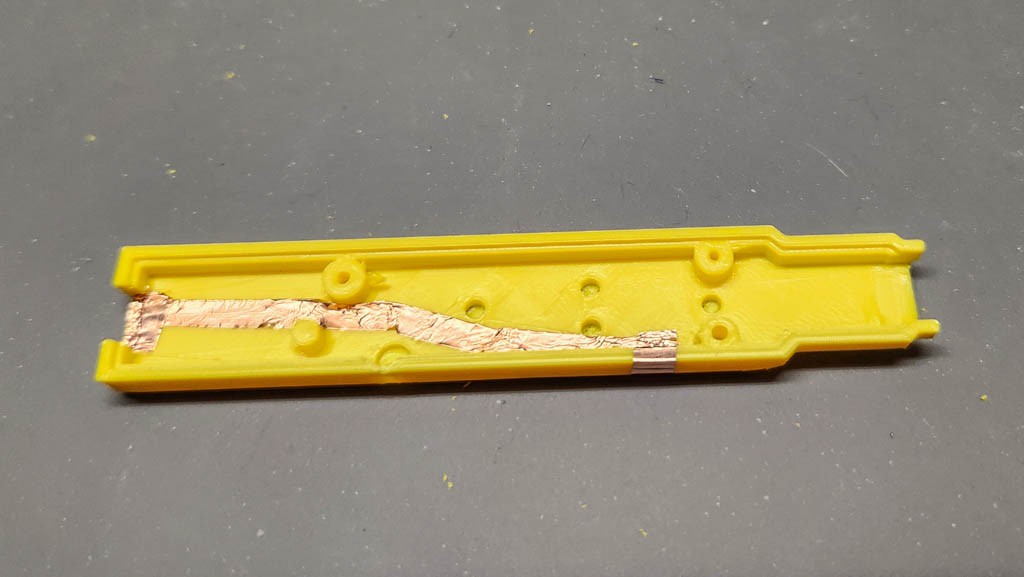
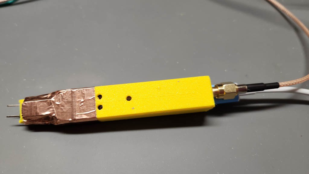
- A 3D printed case, which should allow for reduced sensitivity to external EMI if shielded with some copper tape.
100MHz Probe Specifications (haven't changed from the older version):
- Input impedance: 20MegΩ// 1.25pF - differential, 10MegΩ//2.5pF each terminal to GND.
- Differential Gain = 1/10 V/V. Any lower than this and the DS1102E could not resolve a 1V signal with any clarity. (Many of the cheaper differential probes are switchable between 50X and 500X attenuation. This would be good if the signals in which you are interested are very large, but that's not the case so far with my needs. The better probes ($400 and up) provide 10X/100X attenuation.
- Max AC Common Mode Voltage (with 50Vpp differential input voltage) = 350VAC
- CMRR >90dB @ DC, ~60dB @ 1MHz
- Differential Voltage Range > ±25V for 240VAC common-mode, ±25V for 0V common-mode
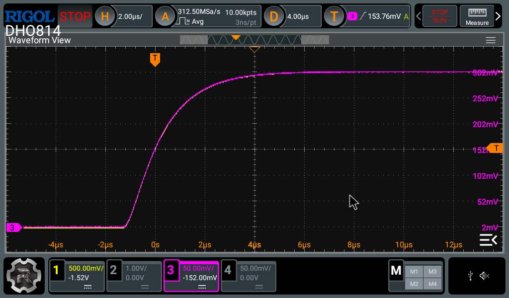
- 3dB bandwidth ≥ 100MHz (Dependent upon signal amplitude)
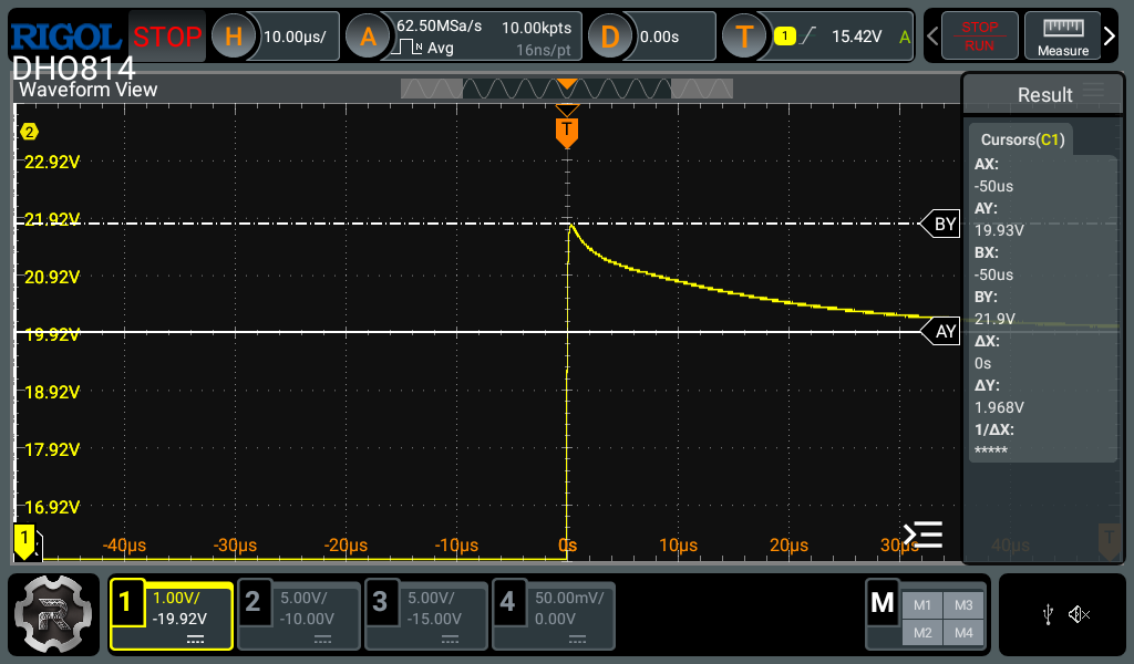
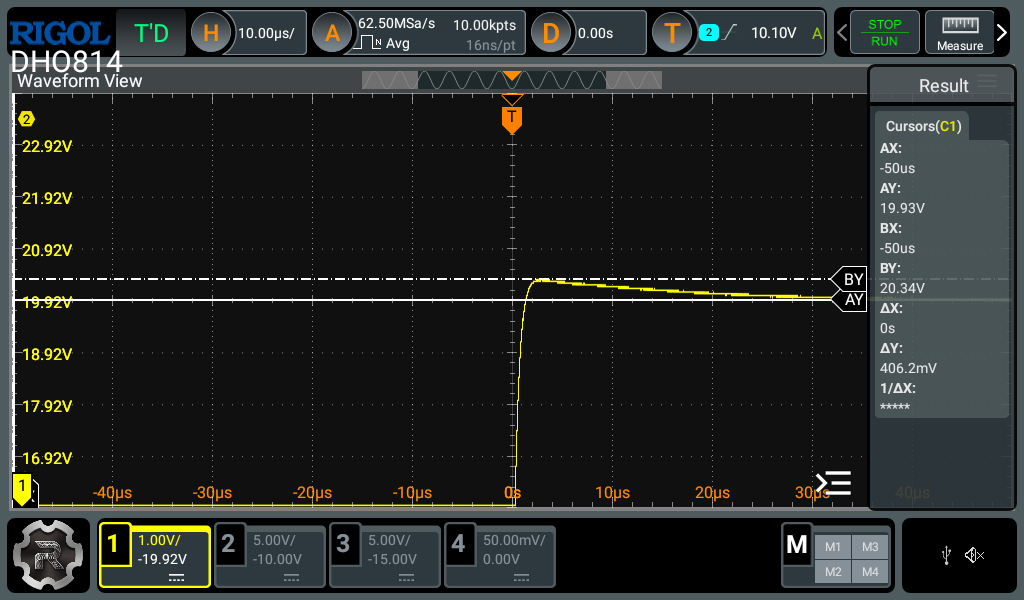
- DC offset < 1mV (trimmed)
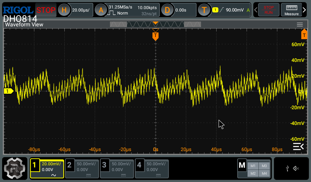
- Noise: 200-300mVpp input referred.
- Input power: 5-5.5VDC @ 60mA.
- Cost: ~ $50-$60
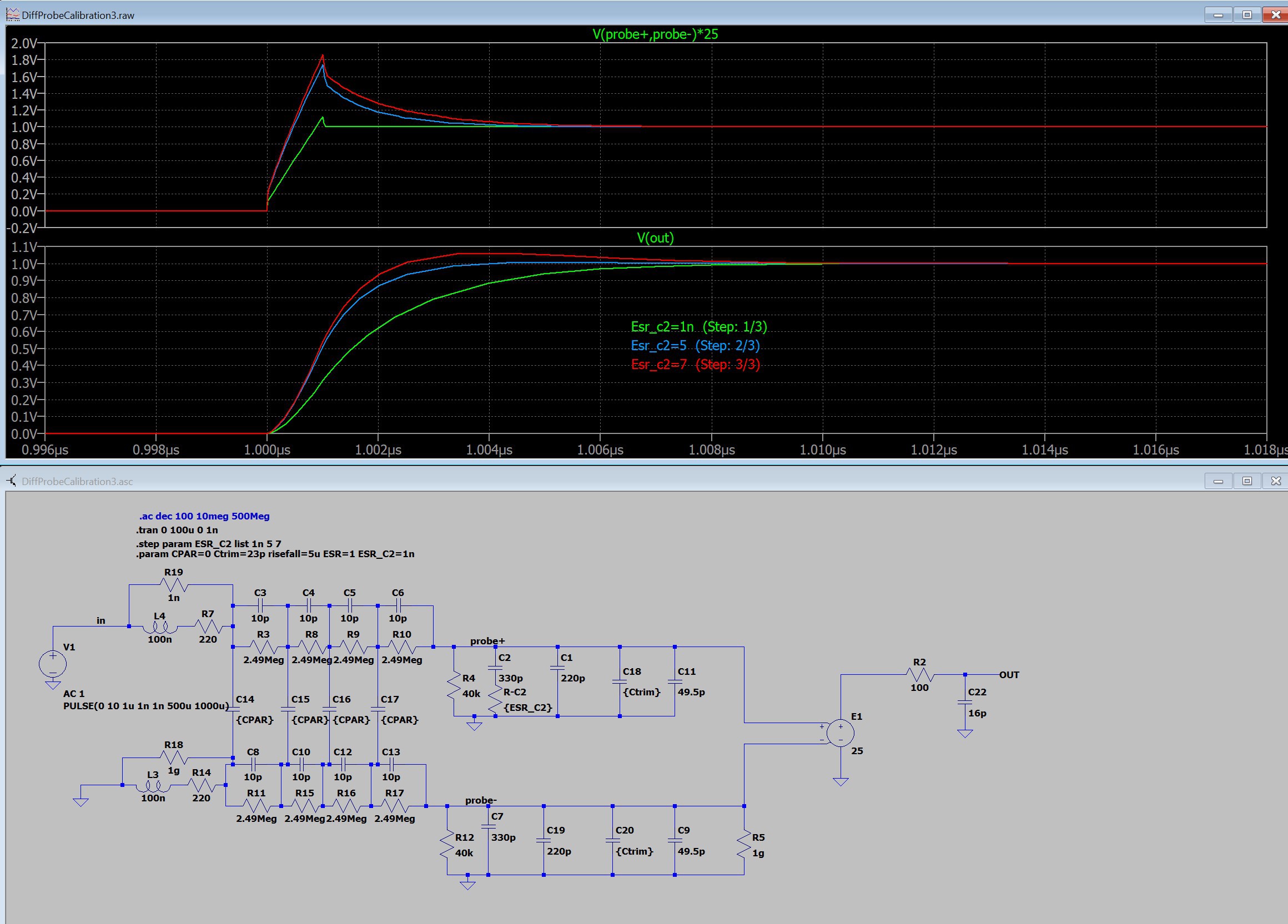
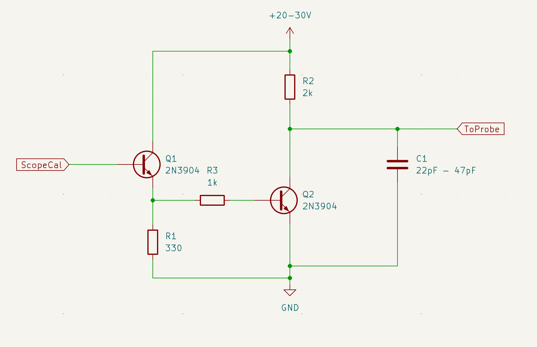
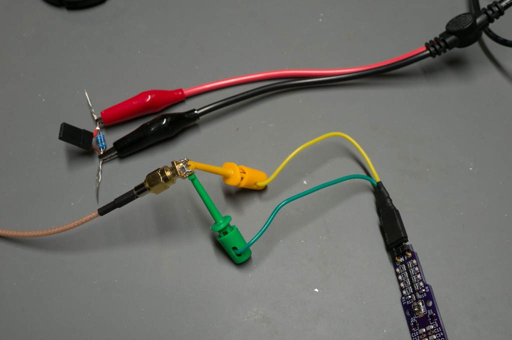
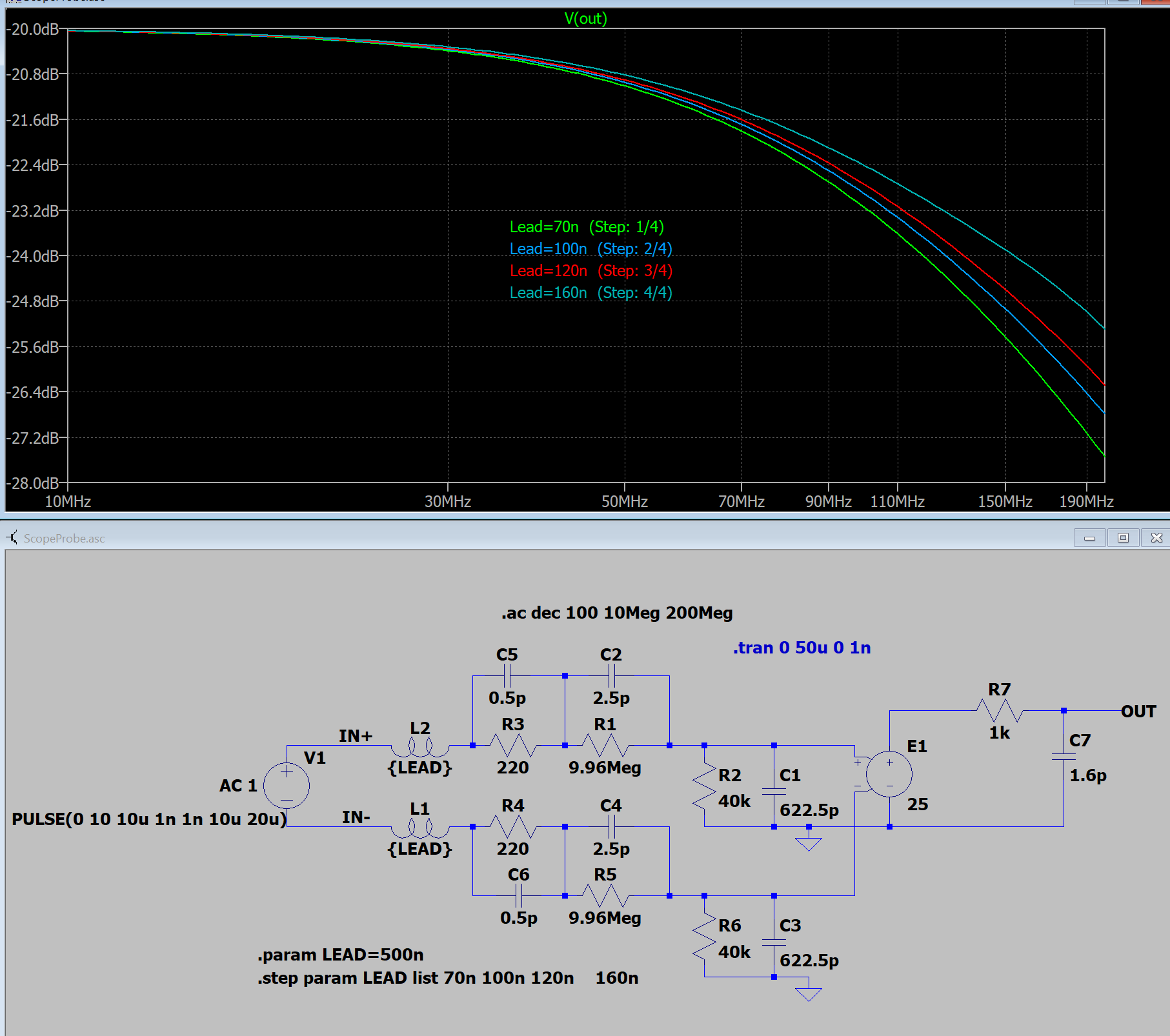
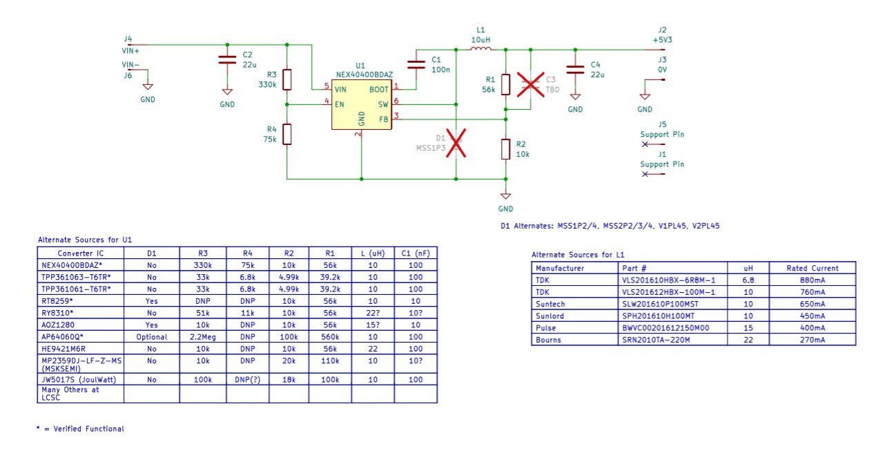
The 100MHz Probe Schematic:
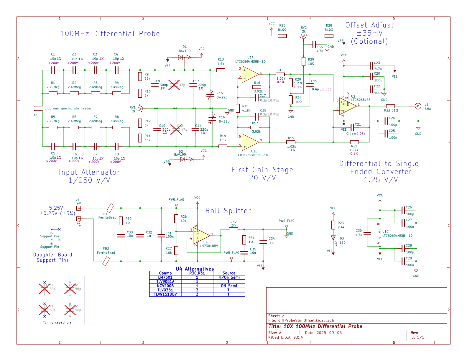
No surprises here. This design was described in gory detail. See the old project.
Electrically, it is nearly identical to the previous design. C1-C4 now connect across to R1-R4 because all of the R's and C's are the same value. Paul added the 4 tuning capacitors so that they would appear on the BOM. C15-C16 were changed to a JR300 trimmer (or cheaper alternative), doubling...
Read more »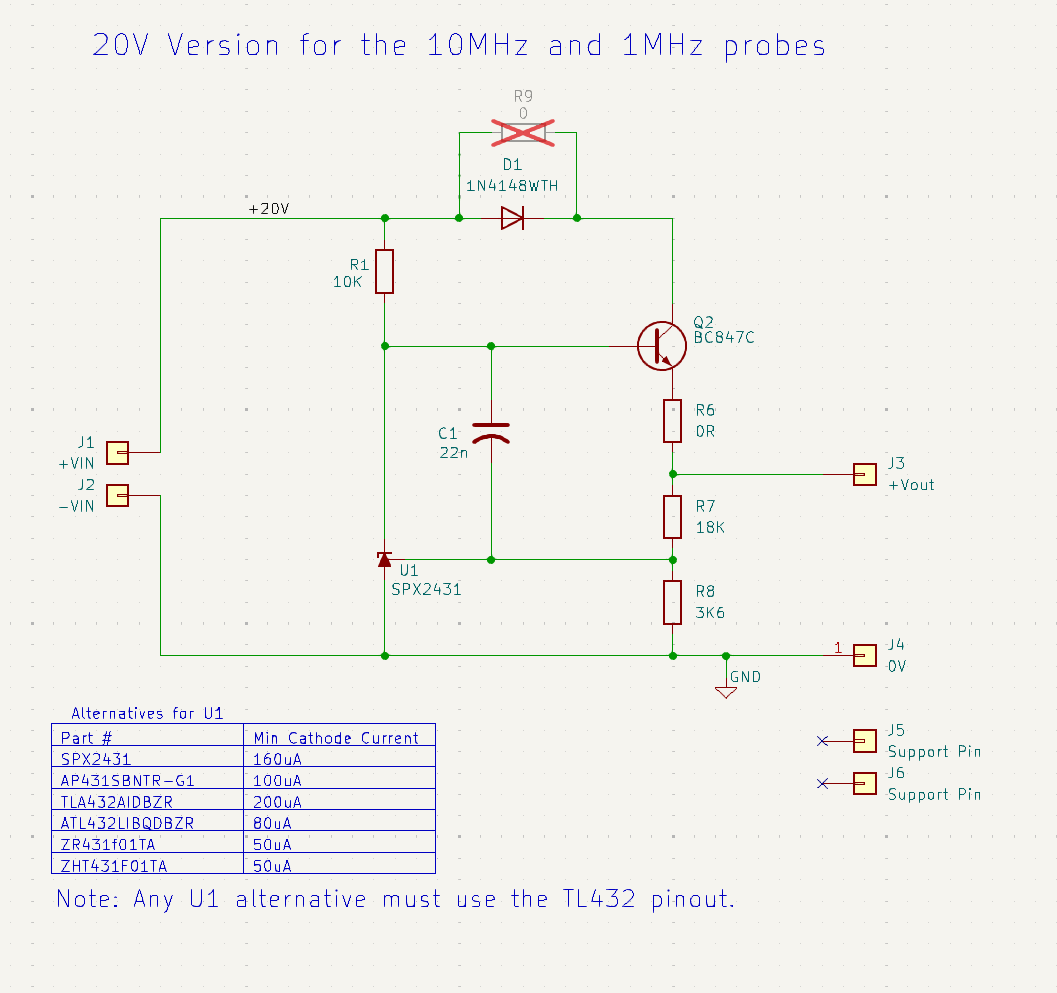


 W4KRL
W4KRL
Hi, I built the earlier version of the project x 3. Really liked it. Using it for comms debugging and power electronics.
Now I was just about to make 10 more for some students. but just noticed the slim update.
where are the project files or when are they coming?
Mounting the 0402 capacitors was hard. but they all works.
Initially the 3 I made only had 10khz bandwidth, but this was solved when I replaced my 51k output resistors with the 50 ohms specified.
Thanks