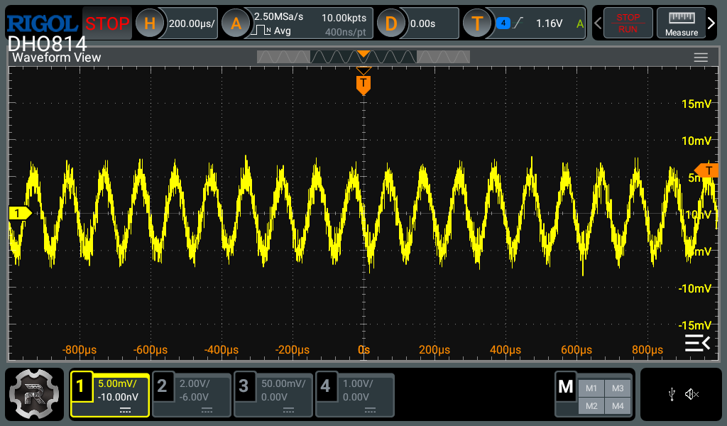
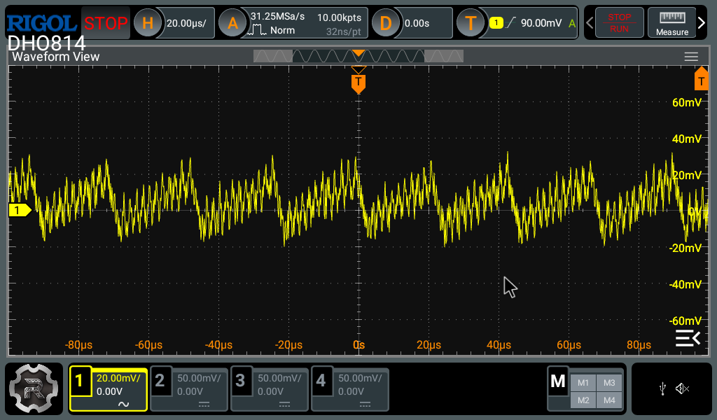
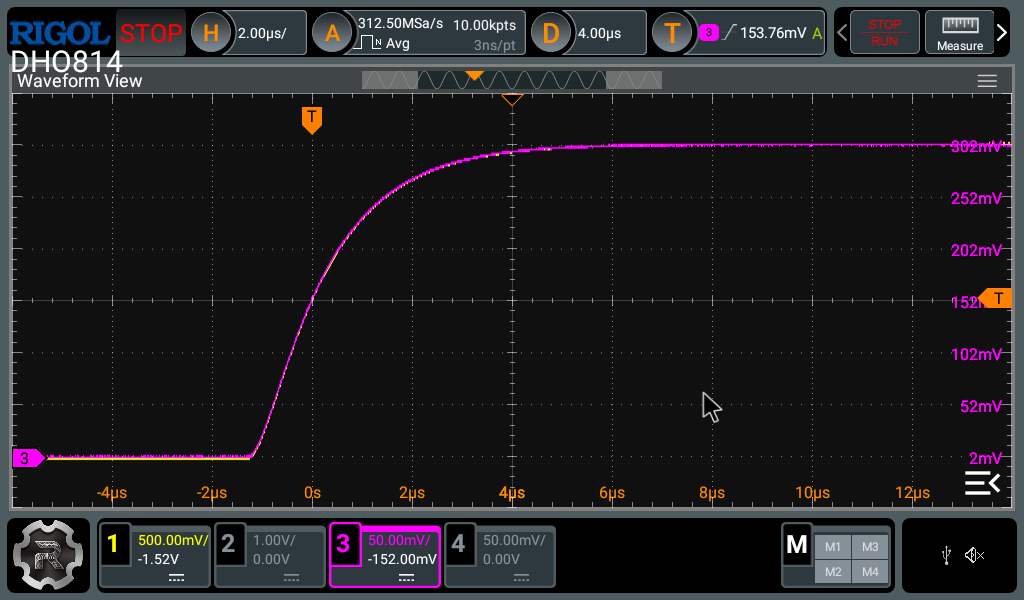
Use a small (<30W) GaN USB-C power adapter. At first, I purchased these adapters from Amazon. They are ridiculously cheap. They worked for the 100MHz probe but did not deliver the required 20V for the 10MHz probe. I purchased this adapter for the 10MHz probe, which works well, and would suffice for all of the probes. Paul opted for a 100W USB-C power adapter that was more suited for laptop computers than phone charging, but even the phone chargers he tried produced too much switching noise. He also tried cheaper adapters, but settled on a 30W GaN power adapter as his final choice -- they have the least amount of switching noise (with a higher switching
frequency) that the on-board filters on the probe can eliminate.. See Paul's blog for details.
There are only two trigger board voltages that make any sense, depending upon your choice of diff probe BW: 9VDC for the 100MHz probe body, and 20VDC for the 10MHz and 1MHz probe body. Choosing 12VDC will result in much higher power dissipation (and heat) with no benefit whatsoever in performance.
Pair the 100MHz probe body with the buck converter daughter board and set the USB-C trigger board to output 9VDC. I think this will yield the lowest power dissipation and coolest operation of the probe. I did not see any evidence that the 2MHz switching noise of the buck converter was visible in the diff probe output. Alternatively, you could pair the probe body with the SOIC daughter board, and trigger board set to 9VDC, if you are concerned about switching noise.
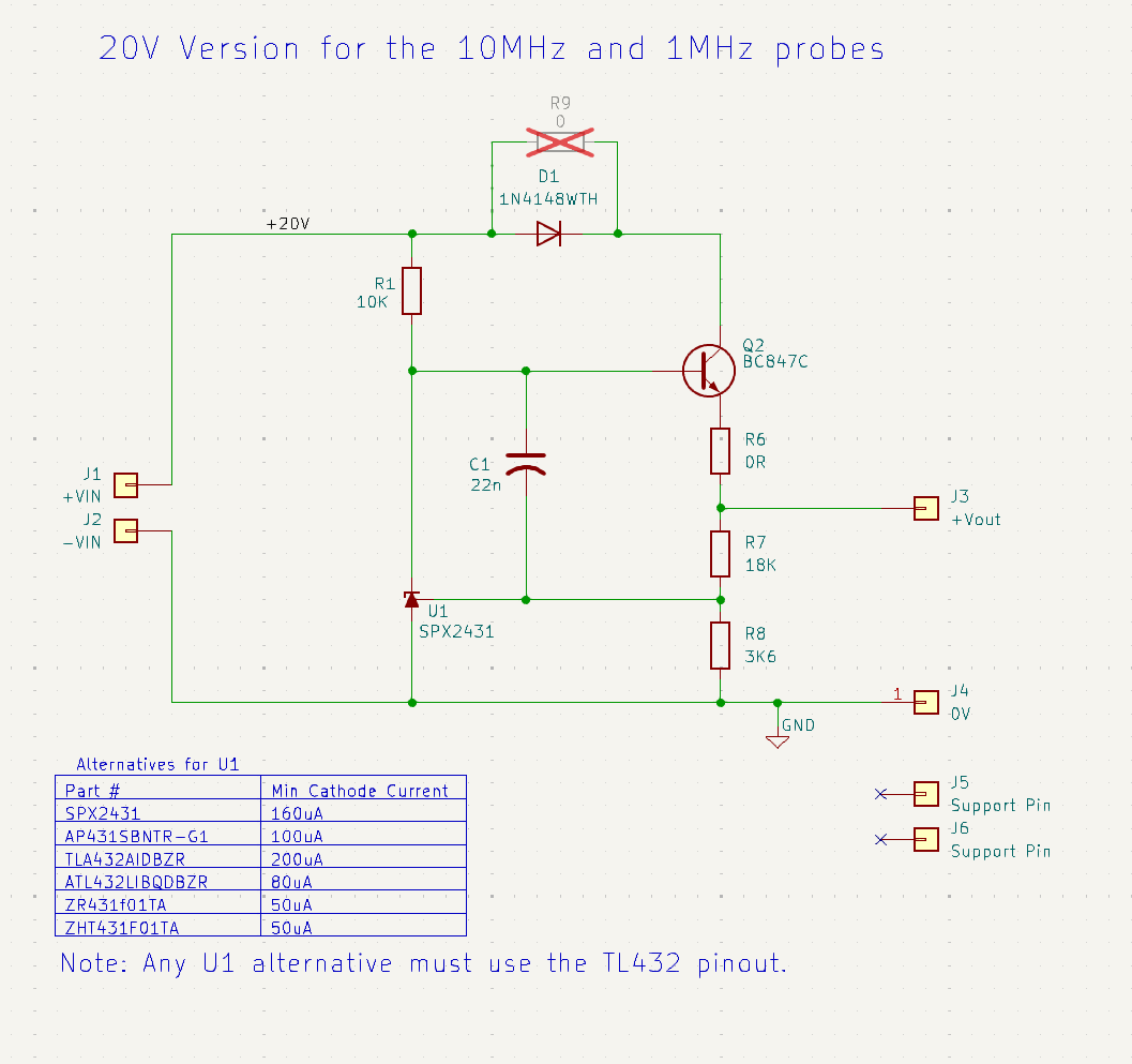
Pair the 10MHz or 1MHz probe body with the depopulated version of the discrete VREG daughter board, or the SOIC8 daughter board. Both of these DBs have excellent tolerance (<0.5%, best case), line and load regulation, and low power dissipation. The depopulated discrete VREG daughter board looks like this: If you don't require reverse polarity protection, then substitute R9 (a 0603 short) for D1.
We don't recommend using the mini USB daughter board or the SOT89 daughter board. The raw voltage provided by a generic USB power adapter may cause the offset voltage of the probe to fluctuate. I found the SOT89 XC6216 LDO to have poor line/load regulation compared to alternatives.
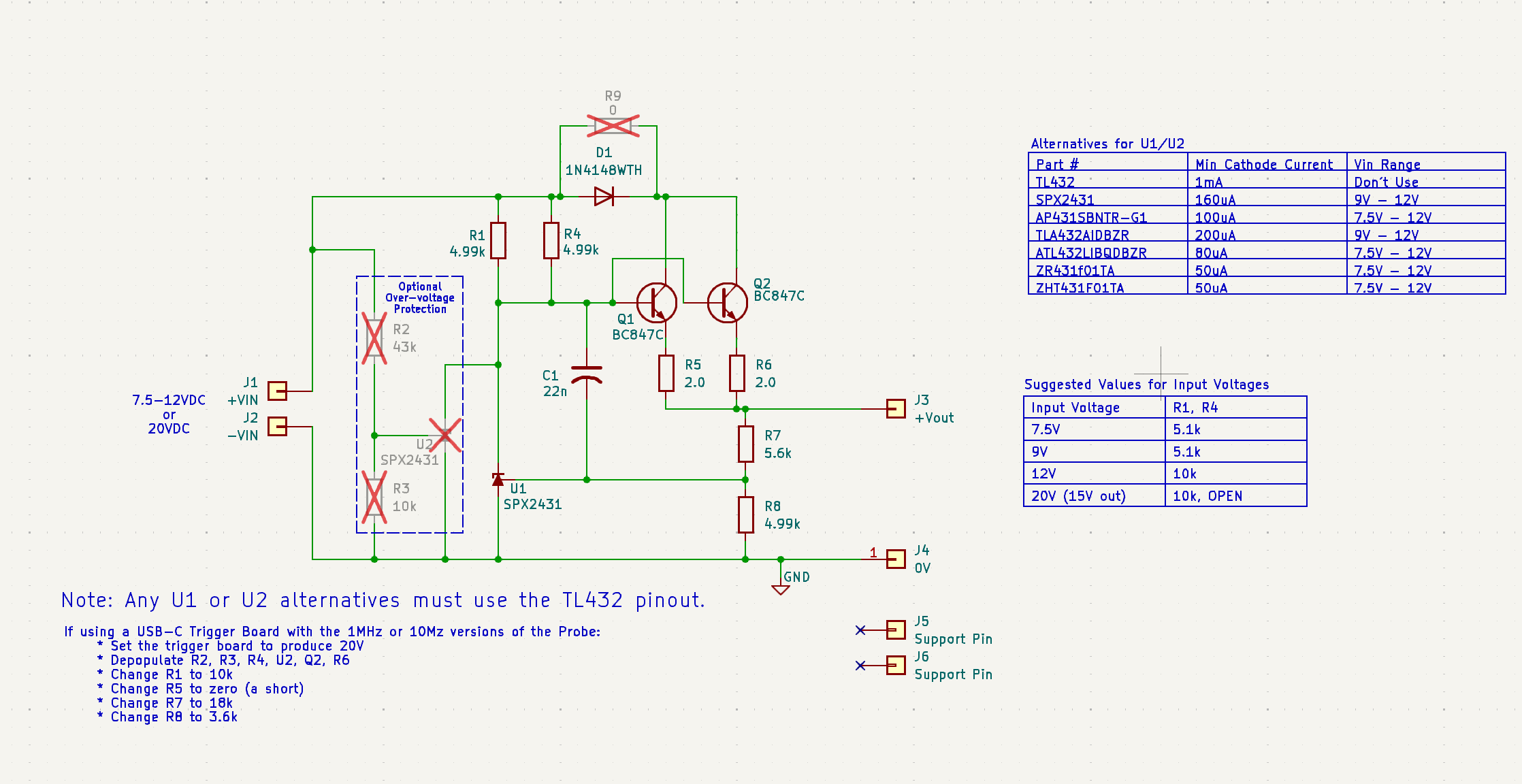
Battery Power: It is much easier to just go with USB-C, but if you insist on opting for battery power, then there are options. For the 100MHz probe Bud would recommend two 4.2V Li-Ion cells and then probably go with the Discrete VREG daughter board since it will work with 6.5V input voltages. The discrete VREG can prevent disaster if you apply more than 12V or reverse polarity. Here's the fully populated discrete VREG daughter board schematic:Paul implemented a battery power scheme with a 9V alkaline cell, again using the discrete VREG daughter board. For the 10MHz/1MHz probes you can stack two 9V alkaline cells, or use a stack of five 4.2V Li-Ion (21VDC), with a depopulated discrete VREG daughter board.
If you are going to build the 10MHz/1MHz versions and you desire more differential input voltage range you can tweak the SOIC8 daughter board to output more than 18V, which would yield +/- 90V. The SOIC8 daughter board uses an LDO that requires much less headroom than the discrete VREG daughter board. Be careful though, there will be more stress on the bypass capacitors. (If you really want to go crazy, the max supply voltage of the OPA2810/OPA810 is 27V.)
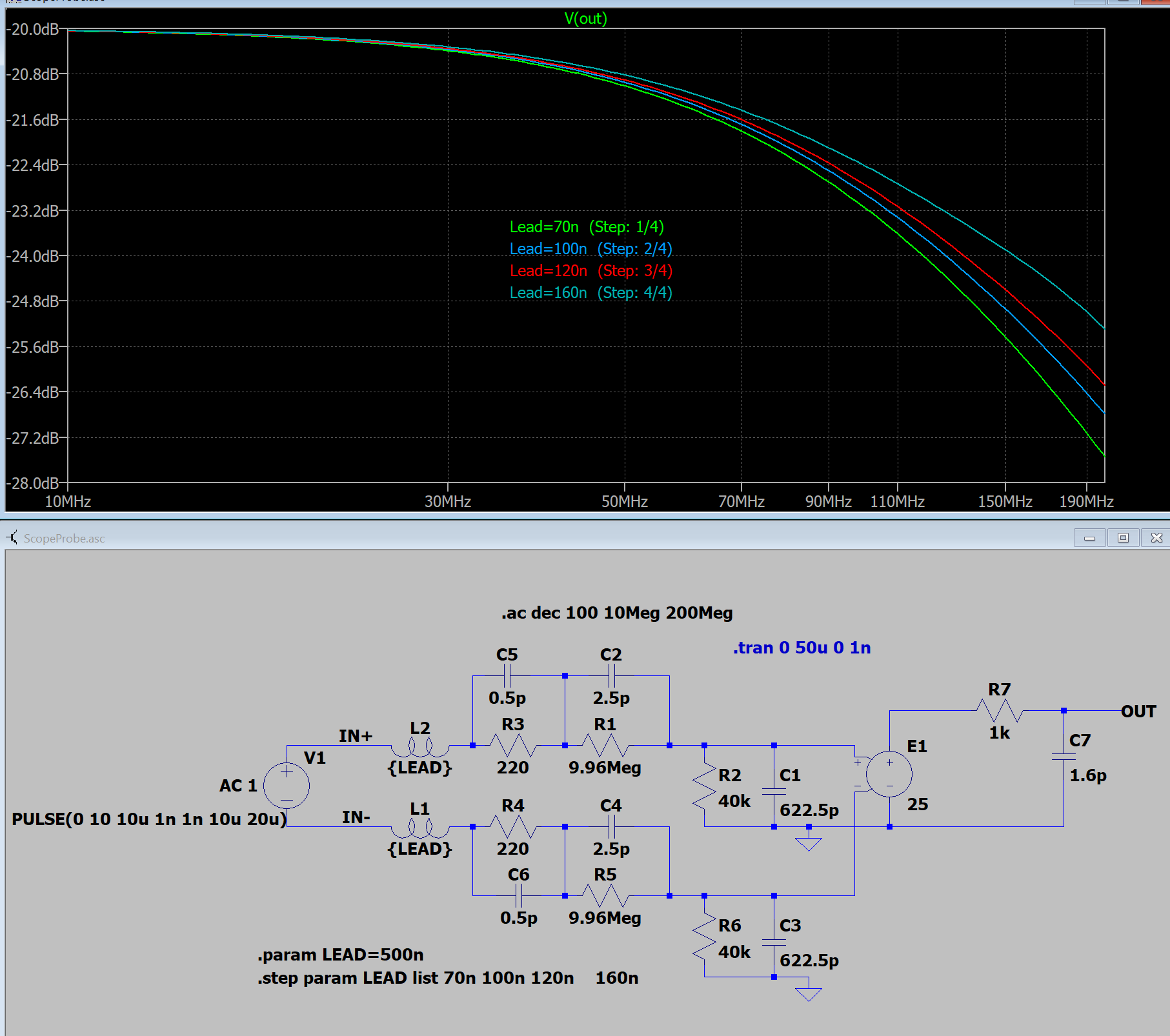
Lead Inductance. See my log about this for more information. If you are going to add some clip leads, make sure to add the appropriate series resistance in each lead. I use 220 Ohm resistors in each of my 100mm clip leads. The other added benefit to the resistors is that they will decrease the probe's loading on a circuit at high frequencies. I calculate the reactive load from a 2.5pF input capacitance is about 640 Ohms. The 220 Ohm lead resistance, along with the lead inductance will likely add another 300 Ohms, for about 1K Ohm at 100MHz. That's 10X better than the 100 Ohm loading from a 15pF scope probe.
Modifications. This architecture lends itself to endless variations in differential voltage gain, differential and common mode voltage range, noise performance, etc. You are on your own if you go down this path. Be aware of the limitations of the layout and the component ratings. You're probably not going to get a 0805 resistor that will withstand 200V, let alone 1kV. If you need more common mode voltage range then you're going to need a different layout with different (and probably more) components to withstand the voltage.
The probe can be used without shielding, but just laying it flat on a bench will cause the CMRR to degrade (or improve). Moving your hand anywhere near the front part of the probe will create parasitic capacitance that upsets the equilibrium of your trimmed capacitors.
I tried several shielding scenarios before settling upon the following. Here's what doesn't work: placing copper tape inside the case -- it is too close, and will disrupt the trim settings beyond what can be compensated; placing copper tape directly upon the under side of the attenuator section of the PCB -- this is a disaster, the copper ground plane was left off this area for a very good reason (but I tried it anyway.)
Paul used a different method to shield his probes. You can check out what he did here.
After you've shielded the probe it will be mostly insensitive to normal handling. By "mostly" I mean that the CMRR will not be affected more than a couple mV when you manhandle the probe. Some of my probes don't show any sensitivity to handling. I did not test it further.
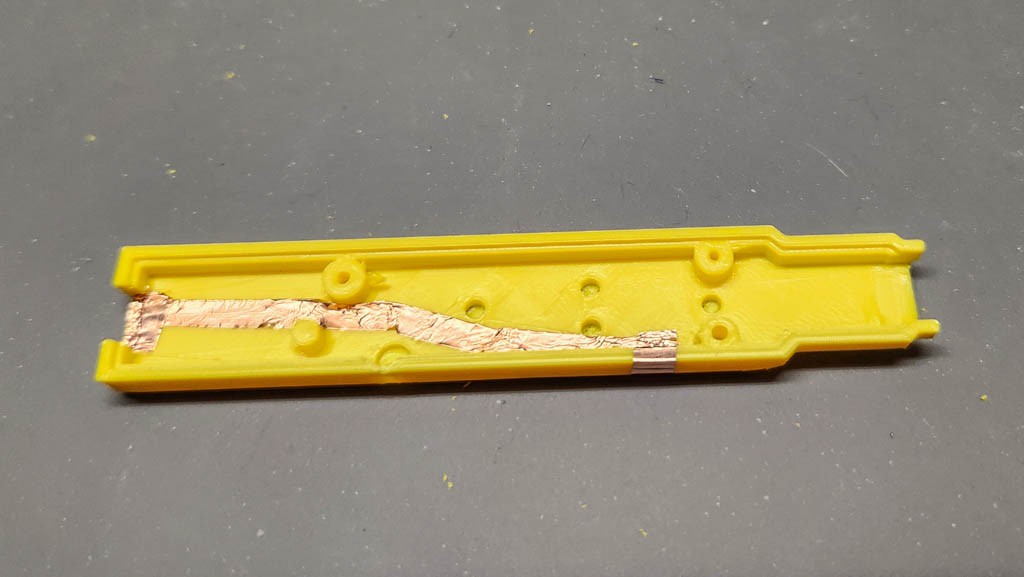
Step 1. Run copper tape from the SMA connector to in front of the two capacitor trim holes, as shown.
There are three pieces of tape in the above fuzzy photo. Use a thin strip to go from the SMA cutout, winding it way to avoid the trim holes and LED area, past the capacitor trim holes. Then put two additional pieces of tape: one to extend the coverage at the SMA cutout, and another to connect the end of the first strip to the outside of the case.
Make sure than these pieces of copper tape are connected with reasonably low resistance. Get out your DVM and measure the resistance from the SMA cutout all the way to the end of the path. If you aren't getting less than 200Ω, then try poking a bunch of holes where the different copper tape sections intersect. You can use your sharp DVM probe tips to do this or a pin. This is REALLY IMPORTANT! If you don't have a GND connection to the shielding then it will not work properly. (Trust me on this. I originally thought that the adhesive for my copper tape was conductive -- it was not -- hence the perforation procedure.)
Step 2. Wrap the area over the attenuator.
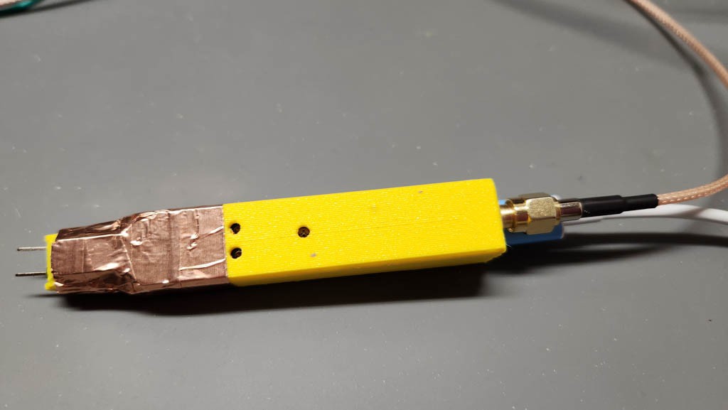
I don't really need to tell you how to do this...do I? Here's a photo of the end result:
I used strips about 10mm wide it's not very pretty, but that's not the point. It gets covered up later. Again, make sure that you have a good connection to the copper tape all the way back to the SMA housing.
Step 3. Redo the Trims.
You need to redo the capacitor trims, and maybe the offset trim at this point. They are easy to access. The DC CMRR trim is not accessible without punching a hole to gain access. You shouldn't really need it if you trimmed it properly previously.
If things don't work out, then you might need to cut the two halves of the case apart and make some more serious adjustments (I did a couple of times.) You can leave the copper tape in place and just place a strip of tape to connect the two halves together -- making holes with pins or probe tips.
(By serious adjustments I mean replacing C11/C12 with smaller capacitors to allow you to get a flat compensation.)
Step 4. Cover It Up.
I used 15mm black heat shrink tubing. It does the job, but I had to stretch it out a bit before slipping it over the shielding. Here's the end result (with a change in color.) I doesn't look that bad, but I'm not showing you the printing on the heat shrink on the other side.
You could also use electrical tape. It is a bit shinier, and a bit less pretty (I tried it.)
Feel free to ignore this and do your own thing. There is no "correct" method. Take the following as suggested procedure.
Step 0: Drill out the holes in the case lid to allow for trimming
I have no pics for this. Just drill out the 4 indentations in the case lid with a 2.5mm drill to allow access later.
Step 1: Solder the PCBs and test them.
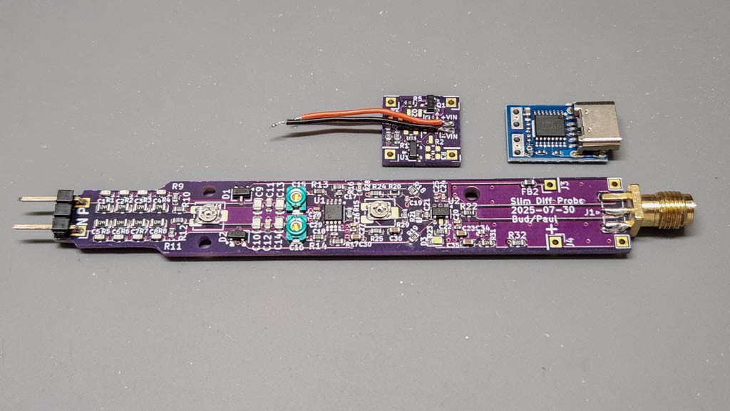
Test all three boards, and make sure that the probe can be compensated (although this could be fixed later.) Solder the power leads that go from the daughter board you are using to the appropriate trigger board. The PCBs below are for the 10MHz probe.
Step 2. Solder the pins to the daughter board.
Try to keep them as flush as possible on the top side of the board. If you have large solder bumps, remove them with solder wick.
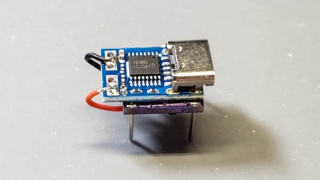
Step 3. Glue the trigger board on top of the daughter board and solder the power leads:
I use a dollop of 5 minute epoxy. Make sure that the trigger board doesn't extend past the front of the daughter board. (A side note at this point. Notice that the USB-C connector extends past the trigger board edge. This will make it easier to fully seat the USB-C cable.)
This trigger board is the shortest one that I know of at present -- it's only 10mm x 16mm. The design will accept a trigger board length up to 23mm, but you might have to change how the power leads are soldered to avoid interference with objects in the case.
Step 4. Solder the daughter board assembly to the probe:
The spacing of the daughter board above the probe PCB depends upon the thickness of the trigger board. I think the most straightforward method is to use the bottom case section to help align the board, as shown below. Get everything lined up and solder the four posts in place. Cut off the excess post material.
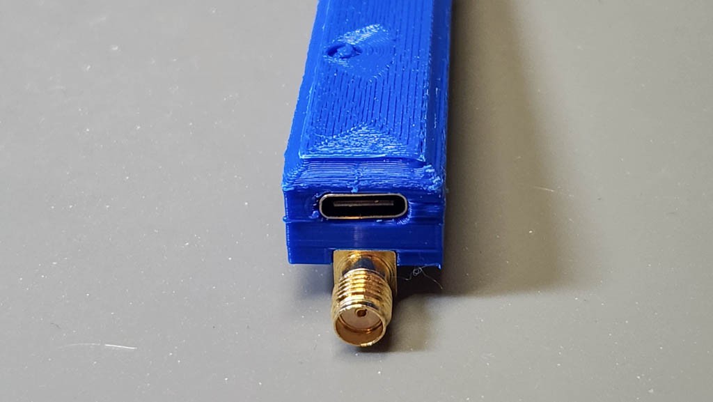
When you assemble the probe body into the case it should fit perfectly:
Step 5. Screw the two halves of the case together.
I don't have any pics of this. I use two M2x10mm screws for the front, and M2x16mm for the rear. Unfortunately, the M2x16 is too long and I must cut it 4-5mm shorter (after cutting threads in the lid first).
At this point your are most likely finished. But you should perform a re-calibration/compensation of the probe before you use it. If you wish to shield the probe from unwanted sensitivities, then read the next log.
I ran out of 220pF NP0 capacitors for the input attenuator, so I substituted with a strip of unspecified 220pF caps that had been in my inventory since I started this hobby some years ago. I think that I got them from Banggood or AliExpress -- very inexpensive -- probably claimed they were X7R or X5R grade. It was a big mistake.
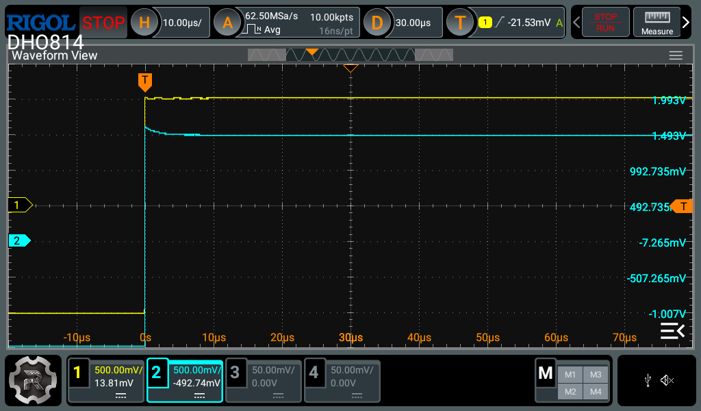
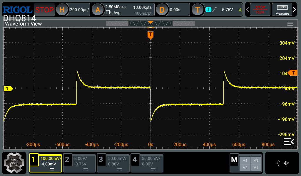
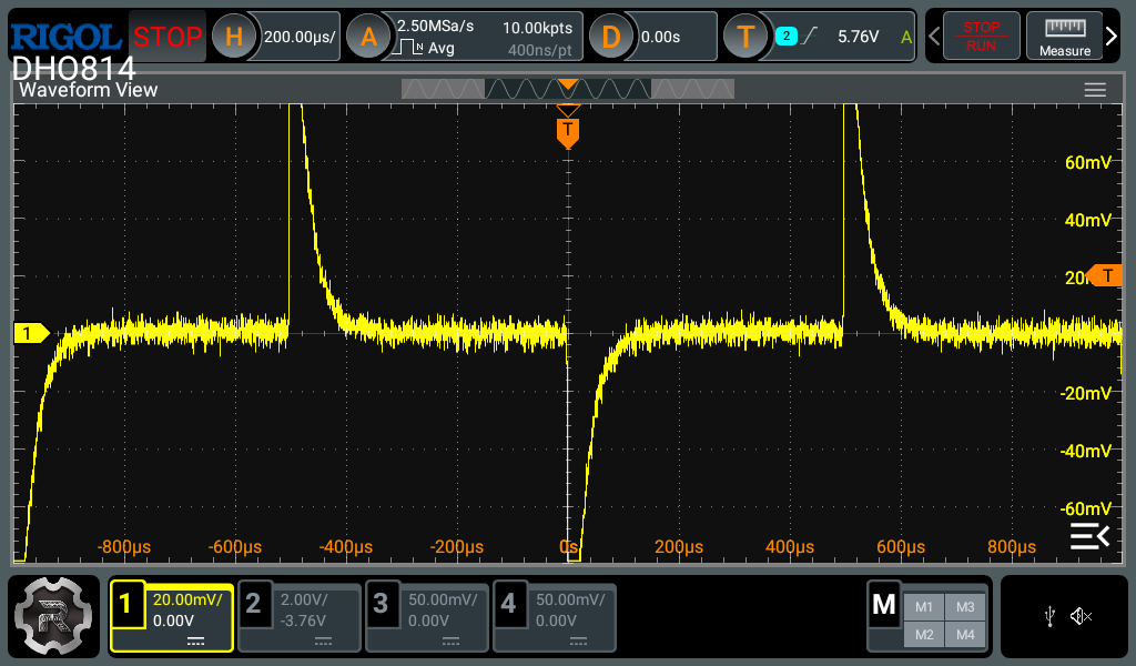
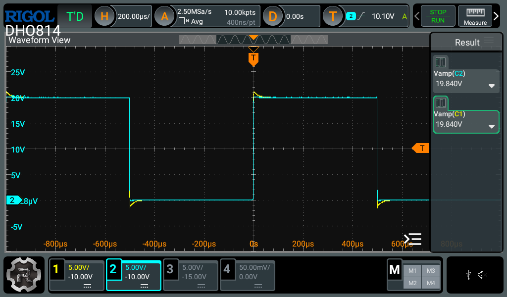
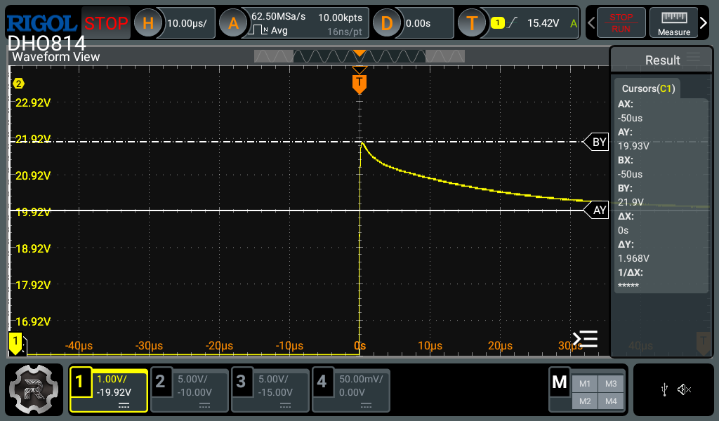
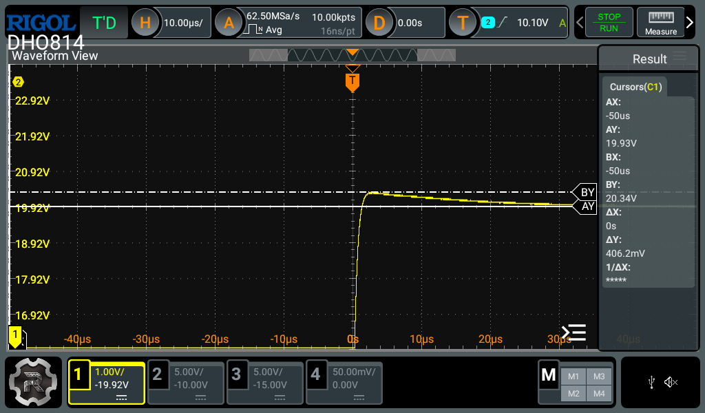
When I tried to compensate the probe there was a short spike at the leading edge of the square wave output that would not disappear by adjusting the trim capacitor. The other odd thing that I noticed was that the spike was constant amplitude and did not change when I was varying the trim capacitor. It looked like this on the scope:
CH1 is the probe input. CH2 is the probe output. Note how short the duration of the spike is -- around 1µs time constant. The probe appears to be nicely compensated otherwise because it is pretty flat after a few microseconds. (The time constant of the attenuator is much longer than 1µs.)
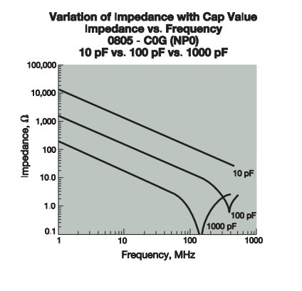
So what caused this? The constant spike size indicates that it is some resistance in the attenuator. Most probably a capacitor with significantly higher ESR (Equivalent Series Resistance.)
When I was looking at capacitor datasheets I found this gem from Kyosera:
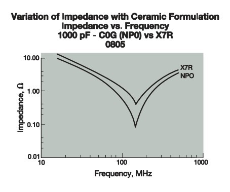
I had always assumed that ceramic caps had very low ESR. Not true for the lower values. And Kyosera offered even more insight:
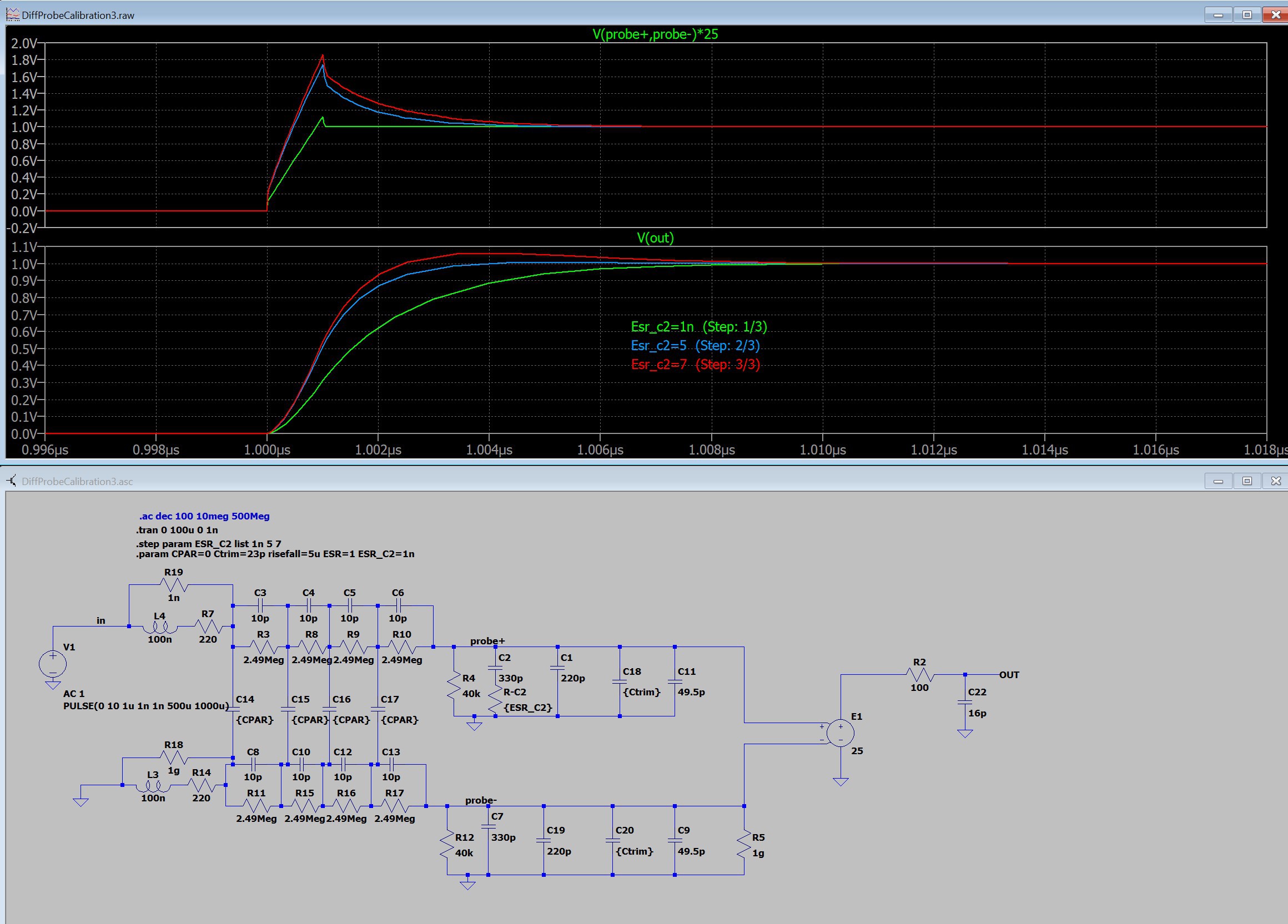
That's a 5x poorer ESR for an X7R ceramic. I set up a simulation to see what LTSpice thought about it. All of the capacitors in the attenuator now have higher ESR to match the datasheets -- somewhere between 100mΩ and 500mΩ. With fast rise/fall edges on the applied input square wave the output shows the spike on a perfectly compensated probe.
I put the extra ESR in series with C2. The spike gets softened by the bandwidth of the probe, but is noticeable as a 3-5% peak. SPICE also indicates that the spike will almost always be present when using extremely fast rise/fall edges.
The takeaway from all of this is to use very good quality capacitors in the attenuator (and probably everywhere else) and slow the down the edges of the waveform used for compensation. That's why I suggest using a square wave with 100-300ns rise times because the spike won't appear and distort your measurements.
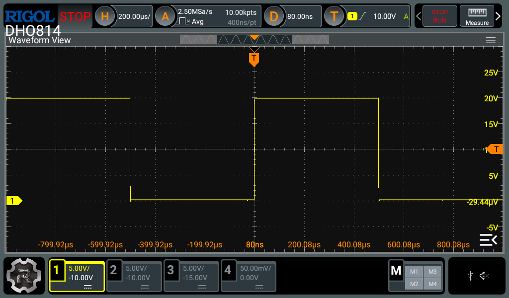
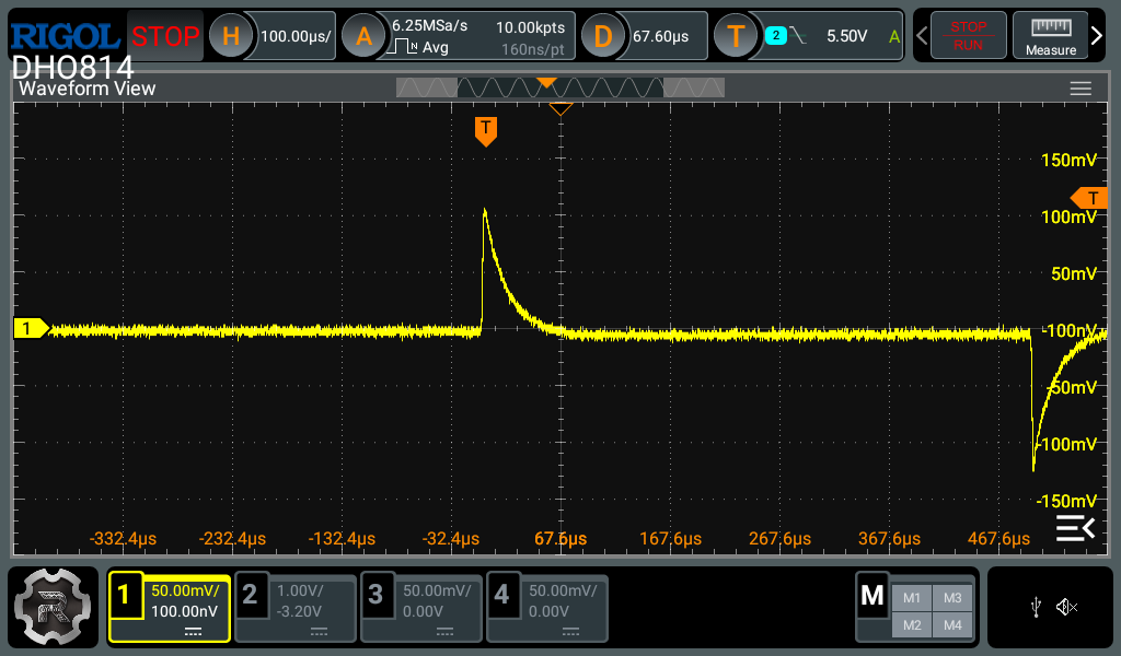
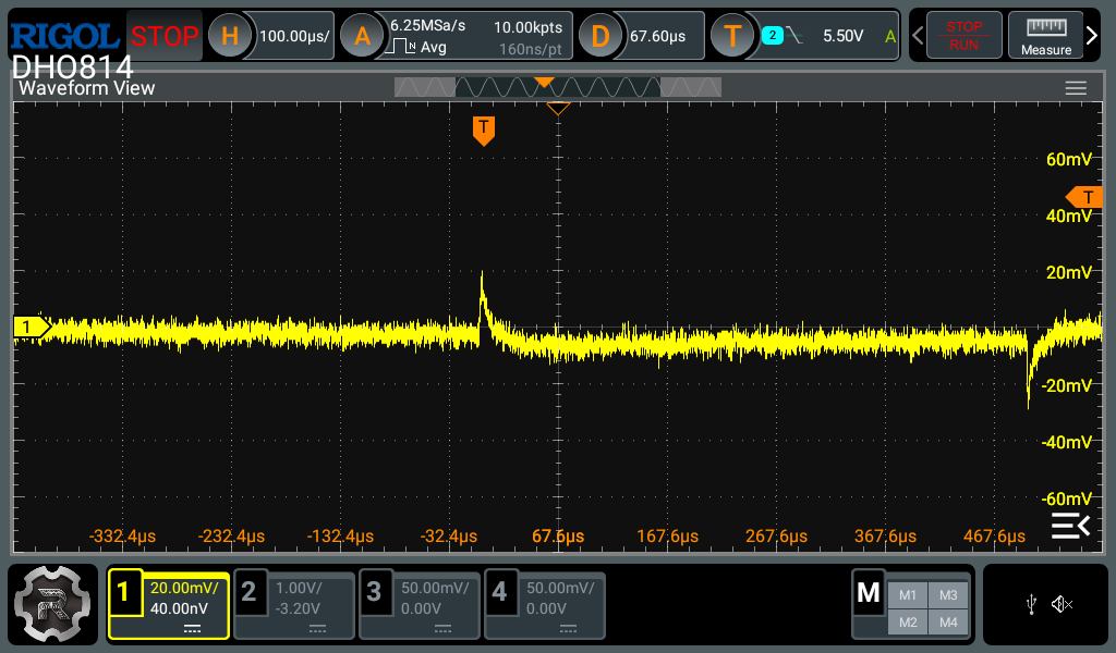
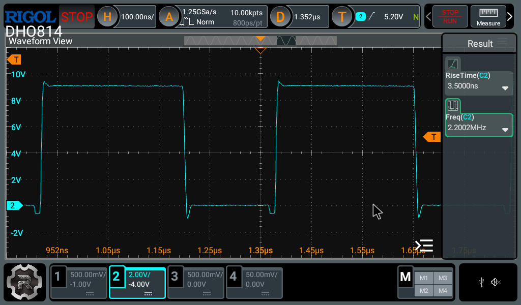
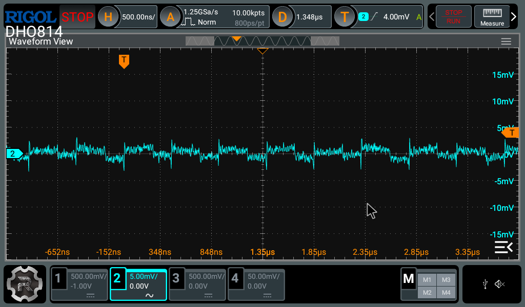
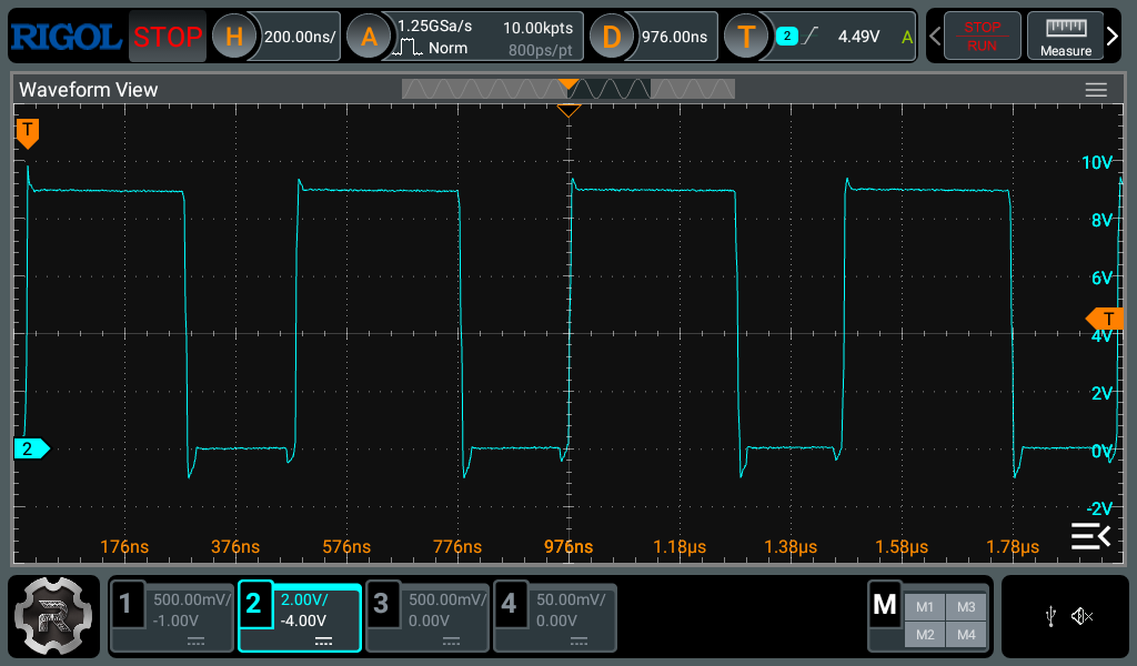
No Spike from the 10MHz or 1MHz Probe:
The effect of the capacitor ESR is evident for frequencies above 10MHz. The lower frequency probes probably won't show this effect no matter how poor the capacitors are.
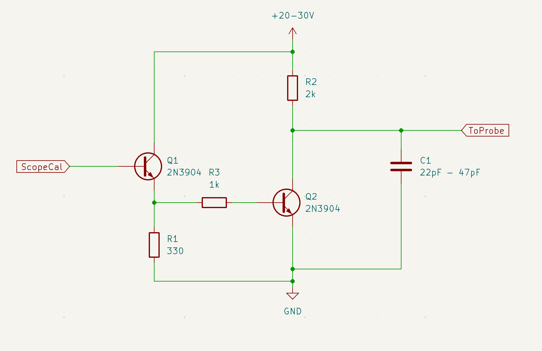
At this point your 100MHz probe is done...except for placing those two last components, C11/C12. Here's what you need to do. If the probe is working then connect the inputs to a suitable square wave source with at least one reasonably fast edge -- a rise/fall time between 100ns-300ns. If it is too fast you might get artifacts from the parasitics in the attenuator. Too slow and you will not be able to determine proper values for the C11/12. I recommend the following circuit, which connects to my 3Vpp/1kHz scope calibration output.
The two 2N3904 BJTs should be easily available, if not already in your kit. You might not need C1, depending upon what medium you use to construct the circuit. It should not be very sensitive to wiring mess ( so just use a plastic proto board.) If you drive it with the scope calibration output the rise time is nearly 300ns. If you drive it with a reasonably fast (<20ns fall time) square wave the rise time is about 150ns. If you hang a nominal 10x scope probe at the output the probe's capacitance will make the risetime slower -- so don't do that.
It is also recommended that only the rising edge be used to compensate the diff probe. The falling edge is not constrained.
Step Number 1 -- Calibrate the DC CMRR:
Connect both probe inputs to your square wave source output. You should see something like this:
Adjust RV1 until the steps are matched. You can ignore the spikes at this point. It is important to match the final voltage values. As so:
Step Number 2 -- Calibrate DC Offset:
Now adjust RV2 until the probe's output offset voltage is removed. If you don't trust your scope's DC levels to be accurate then just connect both of the probe's inputs to the scope's GND and use a DVM. Here's what it should look like when you are probably close enough:
Remember the scope is multiplying the probe output by 10, so this offset reading is well below 1mV. At this level my probe output jumps around a bit, probably due to popcorn noise (1/f noise).
Step Number 3 -- Calculate the Values for C11 and C12:
Here's what a 100MHz probe produced when connected to custom calibration signal:
Use 20Vpp for this test. Channel 1 is the diff probe output (10x) and Channel 2 is a compensated 10x passive probe connected to the same output. The peaks show that the probe's capacitive attenuator doesn't have enough capacitance in its lower leg (i.e. the AC gain is too high), and therefore the signal overshoots a bit and then settles to the value that the resistor attenuator thinks is correct. Channel 2 is just there for a sanity check (that you believe me). I have the scope measuring a swing of 19.84V on the probe output.
Compensating the Positive Signal Path:
You need to measure the overshoot of the square wave signal and figure out how much additional capacitance must be added to the attenuator to make the DC and AC attenuators match. (If your signal is rounded instead of peaked, then you are screwed...the 0805 capacitors are too large and one of them must be replaced with a smaller value.)
Set the trigger for a 10V level (of course this depends upon your scope calibration square wave, or whatever square wave signal you are using now.) The more vertical sensitivity you have the better your measurements will be, but don't overload the scope input to much if you suspect it is becoming distorted. For this example, I'm using 1V/div, with signal averaging set to 32 -- your trigger needs to be rock solid with this amount of averaging.
Adjust the trimmer capacitor, C15, to yield the maximum peak voltage. This will be the minimum capacitance that the trimmer can produce. Measure this peak value. Then adjust the trimmer capacitor to yield the minimum peak value. This is the maximum trimmer capacitance. I used a metal tool to adjust the trimmer cap. When I remove the tool the peaks relax upward. Use your best judgement as to where the minimum and maximum trim points are.
The difference between these two peaks is what the trimmer capacitor can produce. If I want the trimmer range be centered around the flat square wave response, I need to select a tuning capacitor that puts the capacitive attenuator in the center of the trim range of the trimmer cap.
The average overshoot voltage is 1.187V. Therefore the attenuator capacitance of the lower leg is almost 6% below what is needed to center the trim range. (I'm being lazy here, but it's close.) We must take into account all of the capacitances that occupy the lower leg of the attenuator, for which we really don't know those exact values. But here goes in my case: 330pF + 220pF + 20pF (trim cap nominal mid-range -- could be larger) + 3pF parasitic capacitance (due to diodes and opamp input capacitance) ~ about 573pF. So it appears that I need to increase the lower leg of the attenuator capacitance by about 35pF (0.06 * 573pF = 34.4pF). There is some peril is using these numbers because we don't really know what the capacitor values really are (but they should be somewhat close if using 1% tolerances, so let's proceed.)
I dug out a 0603 39pF NP0 cap from my inventory and solder that in C11's place. Here's the result, after trimming for flatness:
That's pretty flat! (Ignore the spike on the trailing edge because the drive circuit isn't very good in that direction...don't ask.)
Flip the probe leads on your square wave source so that the positive probe lead is attached to GND and the negative probe lead is attached to the source. Go through the same steps that you did previously to determine the value of C12. Remember that only only the rising edge (of the input) is useful for calibration.
Step Number 4 -- Compensating the Negative Signal Path to Match the Positive Signal Path:
I'm going to propose a different method to compensate the negative signal path of the probe. The previous method was to just flatten the square wave output of the probe and call it good. That approach may not deliver a good CMRR result at higher frequencies. This new method will improve CMRR at frequencies below where the opamp CMRR dominates.
Find or make a signal source that can swing at least 20-30Vpp at 1kHz. Connect both probe leads to the same signal source output. You will get an output from the probe that looks like this:
Adjust the NEGATIVE PATH trimmer, C16, until the spikes are minimized or disappear entirely. What this last step does is match the AC gain in the negative signal path to the AC gain of the positive signal path. It will probably not be possible to eliminate the peaks. This was my best result (the point where I gave up.)
If you have a sinusoidal source you might be able to improve the CMRR. Connect both probe inputs to a 10kHz 20Vpp sine wave. Adjust C16 to minimize the amplitude of the probe output. You can also adjust C15 to minimize it even further. It won't require much adjustment. Here's what the probe outputs after I went through this process:
That's a 1mVpp swing at the probe output! So CMRR to a 20Vpp 10KHz sinewave is 86dB, or 66dB if it is input referred.
You can test this by switching to a sinusoid source and sweeping its frequency to around 10% of the probe's bandwidth -- 10MHz for the 100MHz probe. If you compensated the probe properly the output of the probe should stay small (CMRR < -50dB) over the entire frequency range.
If you put the probe in a case you will need to repeat the compensation process. The probe should be powered for at least 15 minutes to arrive at a stable temperature within the case.
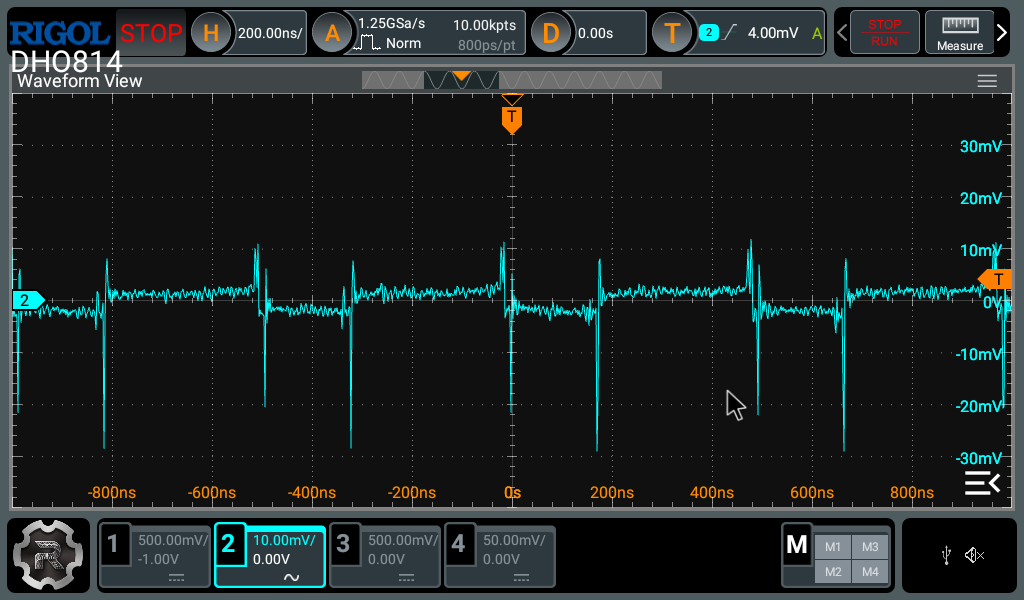
My original list of alternates for buck converter ICs included both the 3Peak TPP361061 and TPP361063. These are 2.2MHz synchronous buck converters with impressive specs at reasonable prices. I soldered the TPP361061 into the buck converter daughter board first. What makes this switcher a bit different is that it uses pulse skipping mode (PSM) at low load currents to keep the efficiency high. The problem is that it would be using PSM with the current levels that the probe uses. The output ripple is not that bad, but it isn't that good either (output load = 82 Ohm):
I measured the efficiency at around 84%, no better than other ICs operating at PWM. So I eliminated this part from consideration.
I then soldered its cousin, the TPP361063 in its place. This is a forced PWM converter...no PSM. When I powered it on with no load the input current indicated it was drawing 10mA. It should have been less than 1mA. Output voltage was correct, but the switching waveform looked a bit wonky. After playing with it a bit I eventually destroyed the only part in my possession. So that one is off the consideration list as well. I did not do anything to the component that I would not normally do to solder it into place. As far as I'm concerned the part was defective when I received it from Digikey, and for $0.50 it is not worth messing with.
It's OK if you want to use TPP361063 in this application, let me know how it performed for you.
I really didn't need to modify the probe for performance issues. This last revision was to allow for two footprints of the trimmer capacitors. I found a cheaper version of the trimmer cap -- SCG3S300 8-30pF, for less than $1/each. The JR300 is slightly smaller, but breaks the bank at nearly $5/each. The other change that I made was to parallel the input capacitor string with the input resistor string. That way the capacitors don't float, which kind of bothered me a bit.
I left C11 and C12 unpopulated and used 300pF and 270pF for C9/C13. This combination was too high and I couldn't compensate the probe. I replaced C13 with a 220pF, which then required C11 to be 47pF to get the attenuator in the range where C15 could compensate. I used a different compensation method, which I will describe fully in another log posting. I powered the probe with a buck converter daughter board using a NEX40400 converter and fed that with a USB trigger board set to output 9VDC.
Supply current with 5.3VDC applied -- 55mA.
Here are some measurement of this latest version:
CMRR @30Hz = -82.5dB (1.5mVpp/20Vpp)
CMRR @ 1MHz = -74dB (1mVpp/5Vpp)
CMRR @ 10MHz = -60dB (5mVpp/5Vpp)
CMRR @ 20MHz = -52dB (13mVpp/5Vpp)
CMRR @ 40MHz = -44.4dB (30mVpp/5Vpp)
These measurement use output voltage/input common mode voltage.
All of the measurements are using 100mm flying leads with 220 Ohm series resistors. Here's a scope trace of the probe hooked to the scope's calibration signal:
It is overlaid CH1 and very nearly identical (but noisier.)
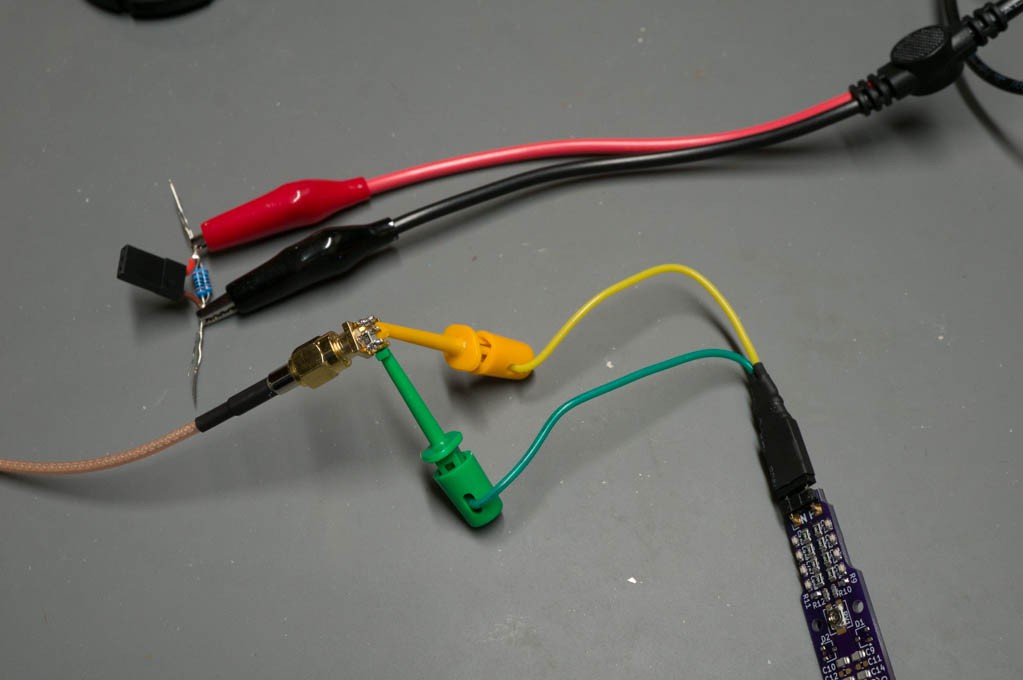
I now have a signal generator, so I can take reasonable measurements to 60MHz. I found that this is trickier than it seems. Any amount of lead inductance will change the result. After several attempts, I eventually followed Paul's approach and soldered a 51 Ohm resistor between the center contact and GND post of a spare female SMA connector as shown below:
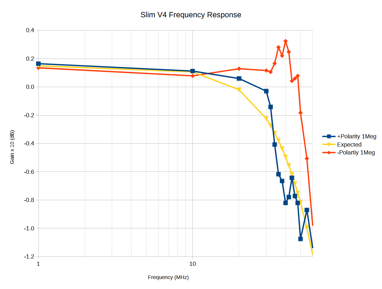
The leads that came with the signal generator caused some weird effects that disappeared (mostly) when I switched to the leadless version. This is what I measured with the probe connected to the 1Meg/15pF scope input with a 30cm coax pigtail.
It's really not as bad as it appears. I plotted an ideal response in yellow for comparison -- using a 51 Ohm termination resistor at the generator output increases the gain by 0.17dB. Remember, a 1 dB drop is less than 10%. It's basically flat until 30MHz. What is odd is that the response of the positive signal path is different than the negative path. The negative path peaks slightly between 30-50MHz and the positive path dips a corresponding amount. I can't explain this, but it is not a huge effect. I suspect that most of it is reflections from an unterminated line into the scope, but the probe is designed for a 1Meg scope input. I performed similar measurements with 50 Ohm terminations at the scope input (with lower signal levels) without any significant change in the result. I also did not see any significant difference between using 100mm flying leads and a very short (~10mm) Dupont connector directly across the signal generator load.
V3 Buck Converter Daughter Board Evaluation:
The purpose of this V3 revision was to add a capability to prevent the switcher from operating until the input voltage is above roughly 6V. The thought is to prevent power applied to the probe when a non-PD compliant adapter is connected and only generates 5VDC. I plan to eventually test at least six buck converter boards populated with different components. To demonstrate that the PCB works I just tested two: NEX40400B IC and the AP64060Q IC. Both converter IC are synchronous switchers that operate at 2.2MHz.
I did not record detailed data, but did get some good results.
The NEX40400B:
This switcher is forced PWM -- that's what the "B" stands for. I didn't think there would be any good reason to have the converter change modes for improved efficiency give that the probe pretty much consumes a constant load current. Used a Sunlord SPH2016 10uH inductor. Under the active load the converter had pretty poor load regulation, dropping from 5.34VDC with no load to less than 5.3VDC with a 70mA load current. It's line regulation was excellent -- less than 2mV change from 7V to 12V applied input voltage. I took scope traces of the switching node and the output ripple voltage. Both were excellent.
Lastly, I checked to see if the converter would prevent operation if the input voltage was too low. The converter did not generate any output voltage when the input voltage was below 6.7VDC. There is considerable hysteresis -- the input voltage has to drop below about 6V before the converter shuts off, which is still acceptable.
The AP64060Q:
I used a different inductor -- Suntech SLW2016 10uH. This converter IC can change its UVLO voltage using a single resistor connected to its EN input. A 2.2Meg resistor sets the UVLO above 6V -- and it works. The line and load responses were both excellent -- less than 2mV change over expected line and load variations. Here's what the switch node and output ripple voltage look like:
The switch node looks very good, but there's quite a bit more spike transients at the output than the NEX40400B.
I covered this topic before for the old differential probe design. I need to revisit this topic because I got it wrong and need to correct it. The other log posting is here. I will be brief.
I was reviewing a few articles on scope probe ground lead inductance when I noticed that many of them called out a 200nH inductance, which seemed too small to me, based upon my previous effort. I decided to check a couple of web-based self-inductance calculators and found that there is an order of magnitude difference between some of them.
The calculator that I used previously, is this one. It calculates the inductance of a 100mm length of 1mm diameter wire is more than 1.5uH. If you consult this other calculator you get 105nH. WTF!
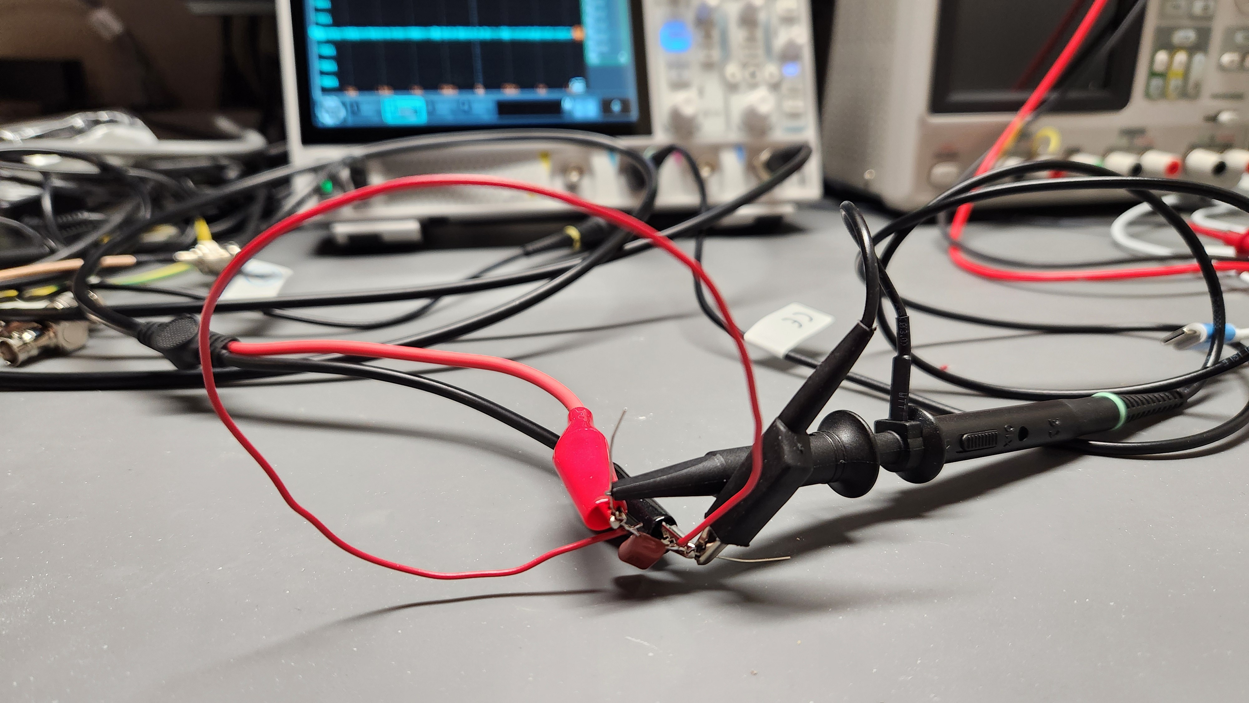
The only way to determine which is correct is to measure it yourself. I took a 250mm length of 26 AWG solid wire, formed it into a loop with a diameter of 8cm and soldered it across a 100nF±1nF mylar capacitor.
Calculator number 2 also has a loop inductance calculator that predicts this piece of wire should be 224nH (308nH if straight). I calculated that the LC tank should therefore have a peak at 1.06MHz. It peaked at 1.02MHz...close enough to verify that calculator number 2 has the proper mojo.
I ran a simple simulation to pick the proper value for the series resistor to de-Q the lead inductance, if using 100mm long leads. It is somewhere between 200-250 Ohms. I picked 220 because that was the closest I had for a 1/8W leaded resistor.
For 70nH - 160nH the output varies 0.8dB @ 100MHz. Good enough. I built as set of these leads and and I can't see any difference (to 60MHz) between the short pins and the longer leads.
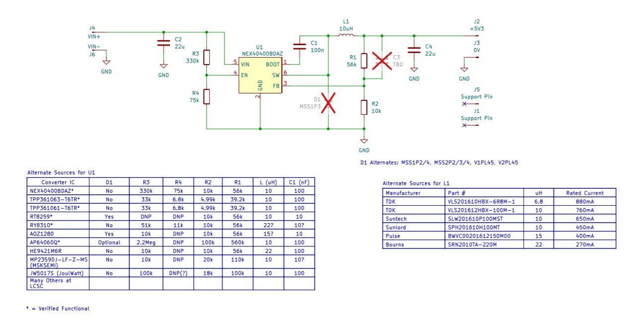
I've finally settled on the topology (and PCB layout) below. It is amazing how many different buck regulator ICs can be used on a fixed PCB layout.
I follow a few simple steps to select components for this design topology:
Pick a suitable IC based upon performance/cost tradeoff.
Pick a range of possible inductors that will be compatible with the chosen IC
Set the desired output voltage with R1 and R2.
Check the datasheet input/output capacitor requirements for value and voltage rating.
Set the value/voltage of C1 from the datasheet.
Sorry about the few choices for the diode. It was in my inventory so I went with it.
Pick IC:
I use Digikey and LCSC (JLCPCB) almost exclusively. Inputting search parameters at both of these websites is more art than science.
At LCSC, use basic parameters to sweep in as many parts as possible. If you set too many restrictions you will get very few candidates. Here is what seems to work (for me) at LCSC:
For category DC-DC Converters: Function=buck, output type=adjustable, Frequency= 1.2-2.1MHz. You can also select synchronous switching if desired. Then select the package types one at a time, SOT23-6, SOT26, TSOT23-6, etc. (If you check them all at once you won't get very many results.) Now you can manually eliminate certain parts that won't tolerate higher voltages > 20V, and by price and availability. For the rest you can click on the datasheet and view the pinout to see if it is compatible. After that run through the feature list and check the efficiency. It's rather tedious. Alternatively, you can just input one of my part numbers into the search bar and see what pops up.
At Digikey, get to the category "Voltage Regulators -- DC DC switching regulators" and select Stocking Options=In Stock, Product Status=Active, Packaging=Cut Tape, Topology=Buck, Output Type = Adjustable, Package/Case=SOT23-6+SOT23-6thin+TSOT23-6. Then select the frequency range -- I use 1.2-2.25MHz. Plug in the quantity you wish to buy to eliminate the minimum quantity candidates. When I did this it produced 91 candidates in order of increasing price. Many of the candidates will not have the input voltage range you need but you can sort them out visually. Finally, check each datasheet for the matching pinout to the layout and proceed to review feature set and efficiency. Alternatively, you can just input the part number you want and get right to the page for it.
The candidate list I created does not pick favorites, but I do have my preferences. Prices start at less than $0.15 for a non-synchronous switcher. I prefer a synchronous switcher -- it's slightly more expensive, but also a bit more efficient and eliminates the cost of the free-wheeling Schottky diode. I went for a lower output current: 500-600mA instead of 1-2A. The current load is pretty modest at 50-60mA, so a smaller set of internal switches will probably yield a better efficiency at lower load currents because the switch transistor gate capacitance will be smaller. I also prefer the higher 2MHz switching frequencies to keep the output ripple current within limits while using a smaller inductor value. It's difficult to justify at 500mA ripple current with a load of only 60mA.
I put question marks in columns where I could not determine the best component value to match the IC. Some data sheets provide a range of inductor values (or even suggested part numbers). Others simply indicate a maximum inductor value for a specific output voltage. And others provide a vague suggestion about larger inductors being better for lower current loads. Having designed these types of switching converters in a previous life, I have thoughts about that. There is a comparator that senses the inductor current and decides when to turn off the switch. If the ripple current is too low, because the inductor value is too large, the comparator might not be able to make the proper decision and a problem ensues.
Just because there is an equation for ripple current doesn't mean that the converter will make it happen. If there is significant delay in the current comparator then the inductor current peak will be larger than intended and the ripple current will be larger. The only way to check for this is via simulation or an inspection of the typical waveforms provided in the datasheet...or when you test it on the bench.
Pick Inductor:
The main constraint is package size -- 0806 (2016 metric). Height doesn't matter much since most inductors of this size will be thinner than 1.2mm. The footprint on the PCB will probably fit all the available candidates. Select a shielded inductor to reduce EMI.
The buck converter datasheet will give a recommendation that inductor ripple current be about 30-40% of the max load current, which is ridiculously small in our case and would call for a very large (>100uH) inductor; or the datasheet will specify ripple current be 30-40% of the max switch current which will work but make the ripple current unreasonably large.
The peak inductor current is given by this equation:
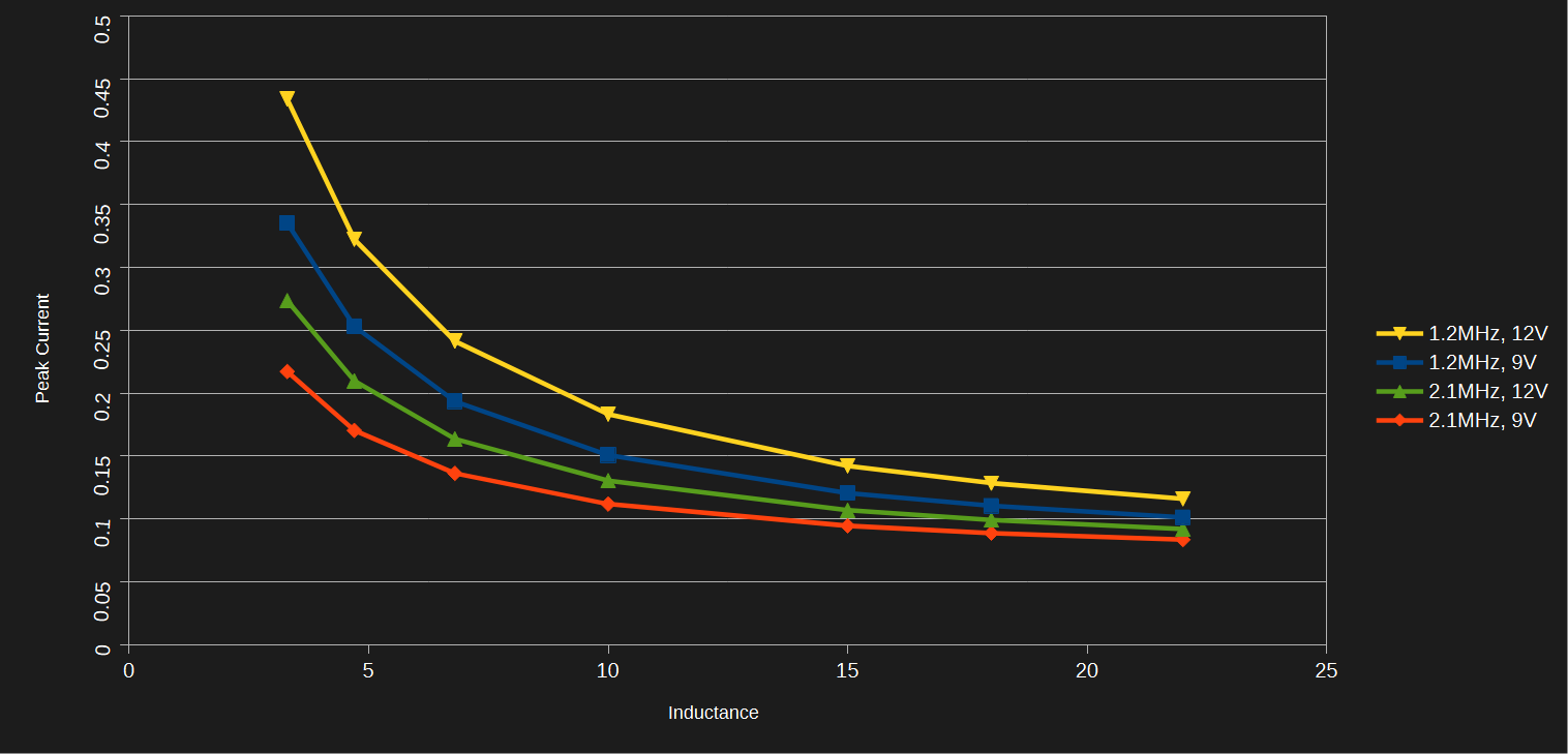
Which yields curves like this for Vout = 5.3V:
Remember to account for the tolerance of the inductor, usually +/- 20%. Avoid small inductors for two reasons -- the larger peak currents will require a larger switch current rating and also cause higher power dissipation in the switches (or switch+diode), input/output capacitors and inductor. You should avoid large inductor values because they will saturate at lower currents and have larger parasitic series resistance which causes power loss. For me, the sweet spot is an inductor value between 10uH and 22uH. The 10uH inductor is a more common value and has better availability. I will also set the USB-C trigger board to output 9VDC.
So now I'm selecting a 2MHz converter and a 10uH shielded inductor with a saturation current above 200mA. The RMS current will be equal to ILoad + Iripple/( 2 * sqrt(3)) = 89mA. The inductor should have a heating related current significantly above this. It's not difficult to find an inductor to meet these specs.
Setting the Output Voltage:
Is straightforward.
Vout = Vref (1+R2/R1)
Check the datasheet for FB input current to make sure it doesn’t impact accuracy. Sometimes the absolute values of R1 and R2 are important if they are part of the overall loop compensation.
Check the output voltage using the maximum value of the reference voltage. Some of these converters have a 3% tolerance. When you add the tolerance of the R1/R2 the result could push the output voltage over the 5.5V maximum. If that's the case, then the target output voltage should be lowered accordingly.
Input/Output Capacitors(C2,C4):
The 22uF 25V 0805 capacitor used for both input and output should not need to be changed. Usually, bigger is better. A datasheet might recommend a smaller input capacitor, or two smaller output capacitors in parallel, to make it easier to obtain the rated voltage in a smaller package size. If the ripple current is reasonably small then a 22uF is plenty big enough for this application.
Boost Capacitor (C1):
It will typically either be 10nF or 100nF. I picked a 50V X7R or X5R rating because it is in my inventory and can be used in other applications. Some datasheets don’t specify a value. That's just sloppiness by the manufacturer. You might want to avoid parts that don’t specify a recommended value for this component. I’ve placed a “?” next to ICs where I could not determine this value. (Yes, the RY8310 doesn't specify C1, but I inserted it into the first pass PCB and it worked well with C1=10nF.)
When I decided to add the 10MHz and 1MHz versions I had to tweak the 100MHz probe a bit. All of the versions use the same PCB layout. The higher supply voltage on the slower versions forced me to change the larger tank bypass capacitors from 0402 size to 0603 because it is difficult to get large 0402 ceramic caps rated above 16V. Also, the input resistor string was changed from 3x3.3Meg + 62k to 4x2.49Meg using 0805 resistors (see reason below).
The 10MHz Probe:
Technically, not a redesign but constrained by keeping the same PCB layout as the 100MHz probe. It was difficult to find suitable opamps. They had to meet the following criteria:
A dual opamp in a MSOP8 (or VSSOP8) with the same pinout as the LTC6269-10, and a single opamp in a SOT26 or SOT25 with the same pinout as the LTC6268.
Supply voltage > 12V (More supply voltage yields a higher differential input signal)
Gain-BW product > 20MHz - 60MHz, depending upon how gain was allocated to the first and second stages.
Slew Rate > 400V/µs. (6Vpeak x 10MHz x 2π)
pA input bias current (for low noise)
Rail-to-rail output swing would be nice.
Less expensive than the LTC6268/9 (this is not difficult).
Needless to say this narrowed the field a bit. After loosening a few of the criteria I finally settled on the OPA2810 and OPA810, which has the following specs:
Available in a VSSOP and SOT25 package.
Max supply voltage 24V
GBW = 70MHz
Slew Rate = 192V/µs
2pA input bias current typical
Rail-to-rail in/out.
Less than $5.00 for the OPA2810, and around $3.50 for the OPA810.
I settled on a 15V supply voltage, which would yield an output swing of 14Vpp with the rail-rail output. Since the gain is set at 1/10 V/V the differential input voltage swing is set at 140Vpp. The higher supply voltage also means that less input attenuation would be required and still meet the common mode range needed, so I decreased the attenuation from 1/250 V/V to 1/100V/V.
I also thought, mistakenly, that reducing the resistance of the attenuator from 10MegΩ to 5MegΩ would reduce the Johnson thermal noise. This increased the input capacitors from 10pF to 20pF to keep the same crossover frequency.
With a GBW of 70MHz the OPA2810 won't have a -3dB BW with a gain above 5 or 6. I set the gain at 5, which makes the second stage gain an easy 2. You want to have the first gain stage as high as possible to suppress input referred noise from the later stages. You also want to have the last stage set the bandwidth of the probe. The max CM voltage x attenuation + max single-ended input voltage x attenuation x first stage gain must be less than 7.25V: 353V/100 + 70V/100 * 3 = 5.63V. The gain of 3 (instead of 5) is because the input is single-ended and has a common mode component to it. If the input signal was differential the max output swing drops to 5.28V.
I had to give up having full bandwidth with a 70Vpeak input swing. The slew rate of the last stage will only allow a 3Vpeak sinusoid without hitting the slew rate limit.
The datasheet suggests keeping the feedback resistors below 2k to avoid degrading the noise performance of the opamp. The max power dissipation of an 0603 resistor is usually less than 0.1W. A quick check on the feedback resistor max dissipation in the second stage = 10.9mW, no problem there. A fat finger check of the total power dissipation of the probe -- 4mA x 3ma/opamp + 3mA (for LED + rail splitter) is less than 250mW. It should be pretty cool.
The bypass caps were changed in accordance with those suggested by the datasheet. This forced a change to the large 2.2μF and 4.7μF capacitors -- changing the footprint to 0603 to make it easier to get them rated for 25V or 35V. (And this in turn caused the update to the 100MHz PCB layout.)
uh..oh...
At this point I found an error in the design of the old diff probe. When I was searching for parts on Digikey and JLCPCB I noticed that all of the 0603 resistors had a max working voltage of 75V. The old design had three 3.3Meg resistors in series with a 62k, so almost all of the input voltage was developed across those three resistors, which exceeded the max working voltage rating. To fix the problem, all of the resistors in the input string must be equal -- in this case 1.24Meg, and their sizes increased to 0805, which increases the max input voltage to 4x150V = 600V. The input voltage requirement is for 360Vpeak + 70Vpeak = 430V. When I changed the resistors to 0805 on the layout I overlapped the courtyards to keep the overall dimensions of the PCB the same.
The 1MHz Probe:
I thought it would be easy to find cheap opamps with GBW > 10MHz and slew rates > 45V/µs, but I gave up when I couldn't find one with the correct package that would take a 15V supply. So the 1MHz probe uses the same opamps as the 10MHz probe and this makes the design pretty simple.
The attenuator is unchanged at 1/100 V/V. Since opamp GBW is a non-issue the first stage gain is raised to 8 V/V, and the second stage lowered to 1.25 V/V, for better noise performance. A quick check to make sure that the output voltage swing of the first stage is still within the supply rails: 353V/100 + 70V/100*4.5 = 6.7V, for a single-ended input.
The bandwidth of the first stage is a don't care -- a 10pF feedback capacitor sets it at 10MHz, but in reality the GBW of the opamp will limit the bandwidth to less than 70MHz/8 = 8.75MHz. The probe bandwidth is then set by the second stage to about 1.5MHz.
Power dissipation is about the same and the bypass caps are the same.
Powering the 10MHz and 1MHz probes:
I suggest to use a USB-C trigger board (set to output 20V) coupled with the VREG daughter board that uses the TL432 shunt regulator design. With this arrangement, the daughter board will only dissipate about 75mW and provide a tightly controlled 15V to the probe. The overvoltage protection and the second pass transistor can be deleted, for a pretty cheap solution. Details about this are noted in the schematic.
Status:
[2025-07-12] The revised probe PCB (V3) and the updated daughter board PCBs are being fabbed at OSH Park. My order of parts to build the 1/10 MHz probe have been shipped.
 Bud Bennett