Jake Robinson
-
Importing a PCB Trace into KiCad
07/27/2025 at 15:14 • 0 commentsShort update for today.
I finished the Inkscape trace and started a process of importing the design to Kicad. Kicad has a tool that converts a picture into a PCB footprint. The idea is to import the Inkscape picture into the tool and convert it into one large footprint.
![]()
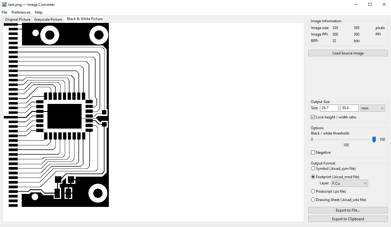
I exported the trace layer from Inkscape as a PNG at 300 DPI. I used this PNG in the image converter.
![]()
This seemingly works as expected. There are some options to configure such as the Black/White threshold and negative output. I bumped the threshold slider all the way to 100. I also verified that dimensions looked correct. I exported this as a kicad footprint with the F.Cu layer selected.
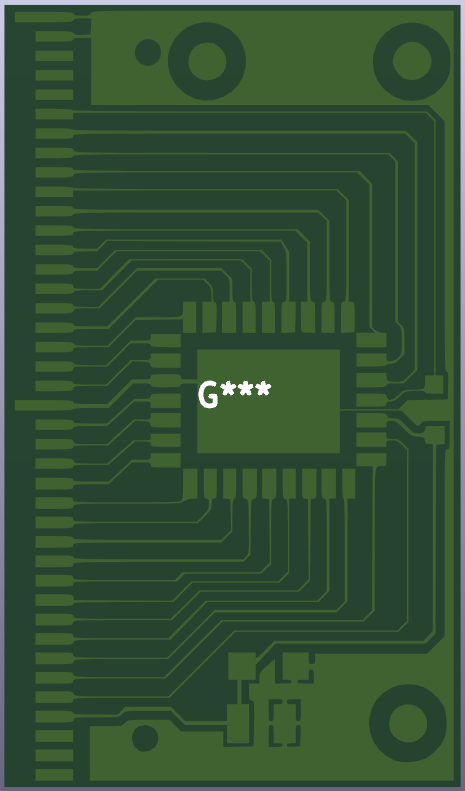
To test the conversion, I started a new project and when directly into PCB layout, imported the footprint and placed it in the design. Zoomed out the footprint looks accurate, but as I zoomed in I could see some approximations in the shape.
![]()
This picture shows the issue. Its interesting how some of the geometry is shown with sharp edges while others have been rounded. The traces are also a little thinner then the original. Not sure where this is cropping up but I plan on looking into this issue for the future. I'm sure someone else has looked into this problem.
Another issue was defining the pads.
![]()
I expected this to be a issue but I'm not certain on the fix for this one. This will be the other topic of research for next time.
-
Tracing the Cartridge PCB
07/26/2025 at 04:08 • 0 commentsOverview
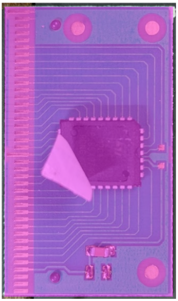
Quick note on a process I am testing to quickly fabricate a PCB using the vector graphic tool Inscape. This log covers tracing a single-sided PCB from the cartridge pictured below. The goal is to take an image of the board and convert it into a file I can send to a board house without doing a traditional layout.
![]()
The picture is not optimal (the sticker is in the way and there are still components on the board) but this test is simple enough that those things should not be an issue.
Process
I am using Inkscape to trace the PCB and a set of calipers to measure the physical board.
To start, I imported the picture into Inkscape and drew a box with the same dimensions as the actual PCB. I used the box to scale the image to its real size. The camera introduced almost no noticeable deformation, which is a good sign for this workflow.
![]()
I created a new layer for the components and another for the copper layer. This should let me export the copper layer to KiCad later.
The result looks like this
![]()
There is a pad on back of the memory component that is not shown here. I will need to add that before moving into kicad.
Conclusions
This first pass shows that tracing a PCB image with Inkscape seems to work well for a small single-sided board with only SMD components. The scaling step was straightforward and the lack of distortion makes the method viable. Next, I want to finish the copper layer and test exporting it into KiCad to see if it can go straight to a board house like OSH Park without any additional layout work.
Analyzing the Brainchild PLS‑1000
a deep dive into its electrical design, components, and architecture to understand this 90s educational device.